
Abstract
Porous GaN films on sapphire (0001) prepared by ultraviolet-assisted electrochemical etching and their quantitative structural characteristics based on mathematical morphology analysis using scanning electron microscope (SEM) images are reported in this study. The evaluation of porous GaN quality can be performed through a non-destructive investigation of its nanostructures using adapting image analysis techniques to obtain rapid, objective and quantitative information. The algorithm used for this work was implemented using the MATLAB software. The distributions of the maximum, minimum and average radii of the pores were obtained. Moreover, the porosity of the structures was obtained by calculating the areas occupied by the pores. SEM micrographs indicated that the shapes of pores for all porous samples were nearly hexagonal. The quantitative results were obtained and related with the characteristics of the fabrication process, showing reliability and promise in the control of pores over the formation process.
1. Introduction
Compared with bulk materials, porous semiconductor materials have attracted special interest because of their unique optical properties as well as their potential applications in optoelectronics and chemical and biochemical sensing.[Citation1–4] The high surface area, band gap shift, luminescence intensity enhancement and efficient photoresponse when the porosity is formed can be tailored to fabricate new sensing devices.[Citation5–7]
The interest in porous GaN arises from the fact that it exhibits unique and superior properties, for example, excellent thermal, mechanical and chemical stability. These special prospects energetically propelled research in porous GaN. In addition, porous GaN can act as a sink for threading dislocations and accommodating the strain.[Citation2,Citation5–7] Besides the management of strain in heteroepitaxy, the manipulation of pore geometries can be used to alter quantum confinement and hence the emission properties of the materials.[Citation1]
Porous GaN can be prepared through dry etching techniques, such as ion milling, chemical-assisted ion-beam etching, reactive ion etching and inductively coupled plasma reactive ion etching. However, these methods could induce surface damage and, moreover, they lack the desired selectivity for morphology, dopant and composition.[Citation8,9] The most feasible and cost-effective method of preparing porous GaN is by electrochemical etching. The main factor in electrochemical etching is the electrolyte. Given the differences in their chemical nature, a wide range of aqueous electrolytes has been used for GaN synthesis. Even so, identifying the optimum etching conditions, e.g. current density, etching time, electrolyte concentration, illumination conditions and so on, is difficult, considering the quality of GaN surface always differs in various growth runs.
In this paper, we report on porous GaN prepared by ultraviolet (UV)-assisted electrochemical etching. This method was employed throughout this work because of advantages such as a low processing temperature, low structural damage, process simplicity, versatility and low processing cost. The sample should essentially be connected to the power supply and biased positive. UV illumination is then used to assist in the generation of electron-hole pairs, where etching proceeds through oxidation, and consequently, the dissolution of the semiconductor surface. Holes play an imperative role in exciting the surface atoms to a higher oxidation state. The supply of holes available on the surface to participate in the oxidation reaction is greatly enhanced by the absorption of incident radiation, resulting in a significantly enhanced etch rate. As a result of nitrogen evolution, bubble formation is observed during the etch process.[Citation10] The dissolution reaction is given by(1)
One of the most important characteristics of porous semiconductor layers is their porosity. Few studies on the porosity of porous semiconductors, conducted using the weighing method, are reported.[Citation11–13] However, this method will cause structural and surface damage to the porous sample. Furthermore, the unintentionally doped (UID) n-type GaN films grown using the metalorganic chemical vapour deposition (MOCVD) technique are generally thin, very complex layers. Given these reasons, attaining a generalised porosity measurement based on the conventional measuring methods is unfeasible. This fact is therefore an impetus for developing a method of estimating general fabric porosity via image processing techniques, which, to the best of our knowledge, to date, has only been reported by Ahmed et al.,[Citation14] though only at an initial stage. Further experiments need to be performed to determine which method is more accurate.
2. Experimental
2.1. Porous preparation
The commercial UID n-type GaN film grown by MOCVD on a 2 inch diameter sapphire (0001) substrate was used in this study. The thickness of the GaN film is 3 μm with carrier concentration of ∼6.05 × 1017 cm−3, as determined by the Hall effect measurement. The wafer was then cleaved into a few pieces. Prior to the metallisation, the native oxide of the sample was removed in the 1:20 NH4OH:H2O solution, followed by 1:50 HF:H2O. Subsequently, boiling aqua regia (3:1 HCl:HNO3) was used to etch and clean the sample. The porous GaN in this work was generated by UV-assisted electrochemical etching.
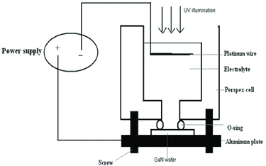
For the generation of porous GaN, an aluminium mask (circular pattern), 0.8 mm in diameter, was applied over the GaN surface as front contact for all the samples, which provided an ohmic contact. In the anodic etching process, platinum was used as a cathode electrode. The GaN sample was connected by a copper wire to the power supply and biased positive with varying current densities of 20, 40 and 60 mA/cm2. A 500-W UV lamp and 4% KOH electrolyte concentration were used during this experiment at a constant etch time of 30 minutes. After the chemical treatment, the samples were removed from the solution, rinsed with distilled water, and dried in ambient air. Synthesis was performed at room temperature. The typical electrochemical cell for the generation of porous GaN is schematically shown in Figure. The surface morphology and structural properties of porous GaN were investigated by a scanning electron microscope (SEM; JOEL JSM-6460LV) at 10 kV.
Figure 1. Schematic of UV-assisted electrochemical etching apparatus.
2.2. Image processing method
The resulting SEM images need to be converted to output binary image (BW) that has values of 1 (white) for all pixels in the input image with luminance greater than LEVEL and 0 (black) for all other pixels. (Note that LEVEL is specified in the range [0, 1] despite the class of the input image.) Some of the filtering, such as adaptive noise-removal filtering, has to be applied to the image and the low pass filters an intensity image that has been degraded by constant power additive noise. Moreover, the fundamental operation of the mathematical morphology is Wiener2 which uses a pixel-wise adaptive Wiener method based on the statistics estimated from the local neighbourhood of each pixel.
The algorithm used to estimate the local mean and variance around each pixel is(2)
(3) where n is the N-by-M local neighbourhood of each pixel in which the image then creates a pixel-wise Wiener filter which is created using the following estimates:
(4) where ν2 is the noise variance. If the noise variance is not given, Wiener2 uses the average of all the local estimated variances.
We bound the holes to trace the outer boundary of objects, as well as the boundaries of holes inside these objects, sequentially to identify the number of holes (black holes). This also descends to the outermost objects (parents) and traces their children (objects completely enclosed by the parents). BW is a binary image where non-zero pixels are the objects and zero pixels are the background. Initially, using some technical code, for instance, finding the area of each hole using estimates of the areas of the objects in a binary image (BW), we separated the holes according to their diameters. The total sum is a scalar with a value corresponding roughly to the total number of ‘on’ pixels in the image but possibly not exactly the same because different patterns of pixels are weighted differently. The determination of the hole diameters became uncomplicated after determining their areas. Finally, the plot tools in MATLAB version 7.4.0.287 (R2007a) were used to obtain the results and arrangements according to the diameters in nanometres. The flowchart of the program is shown in Figure.
Figure 2. Flowchart of the MATLAB program.[Citation14]
![Figure 2. Flowchart of the MATLAB program.[Citation14]](/cms/asset/676767f3-f33a-4caf-9333-90ed12610713/tjen_a_814173_f0002_b.gif)
3. Results and discussion
3.1. SEM
SEM images of the porous GaN samples generated under different current densities are shown in Figure. The SEM images in Figure(b)–(d) show well-defined layers of pores with different sizes due to the monocrystalline epilayer structure of GaN. Apparently, etching first occurred at the centre of the grain structures with the grain boundaries remaining un-etched, considering grain boundaries are mostly defined by threading dislocation.[Citation15] For the 20 mA/cm2 sample, the etching was at the initial stage: pores started to form and mostly hexagonal-shaped structures were observed. This finding is ascribed to the etching rate in the crystal centres, which was slow enough to allow the grain boundaries to be etched at an adequate rate. When the current density was increased to 40 mA/cm2, the surface became very regular and relatively rougher. Last, for the 60 mA/cm2 sample, more uniformly hexagonal pores were gradually formed on the entire surface of the sample. Furthermore, the pore structure was confined to a smaller size, as seen in Figure(d). Therefore, when the etch rate is too high, the grain boundaries are etched significantly slower than the centre of the crystals.
Figure 3. SEM images of different samples: (a) as grown (b) 20 mA/cm2 (c) 40 mA/cm2 and (d) 60 mA/cm2.
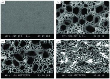
Interestingly, however, the porous GaN prepared by electrochemical etching did not always produce a similar surface morphology. Several groups [Citation10,Citation16–19] fabricated porous GaN by anodic etching. The porous GaN produced by Hartono et al. [Citation15] was covered with hexagonal pores whereas those produced by Yam et al. [Citation20] were covered with star-shaped, elongated, triangular and squarish pores. Moreover, the average pore size was more sensitive to electrolyte concentration than current density.
3.2. Porosity measurement
Our aim is to present the quantitative structural characteristics of a porous GaN layer based on the proposed algorithm applied to the SEM images. The new algorithm computed the size distribution of the pores and classified the pores in nanometres. The new image-processing (IP) algorithm is shown to be an effective tool for SEM images processing to analyse quantitatively the porous materials’ parameters.
Based on SEM images, a number of parameters and their distributions can be measured using image analysis techniques. The SEM images of the porous GaN layers prepared under different anodisation current densities and the same magnification at 50 k are shown in Figure. The SEM images revealed that pore distribution is dependent on the current density. The new algorithm for computing GaN porosity revealed that for the as grown sample, less than 1% defect porosity was observed. For the 20, 40 and 60 mA/cm2 samples, the porosity were 30.6%, 37.8% and 43.2%, respectively. These measurements showed that porosity strongly depends on the current density and highly affects the surface morphology of the etched samples. The image processing results of porous GaN and as grown sample structures are shown in Figure.
Figure 4. Image processing results of porous GaN structures.
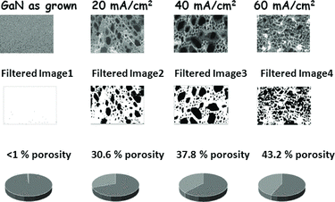
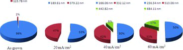
Figure illustrates the output defects of our algorithm for porous GaN and as grown samples etched under different anodisation current densities. For as grown GaN, the majority of the pores have a diameter of 123.78 nm. On the other hand, for the 20 mA/cm2 sample, 53% of the pores had a diameter of 189.61 nm whereas the rest had a diameter of 379.21 nm. Notably, for the etched GaN sample with current density of 40 mA/cm2, nearly half of the pores had a diameter of 166.06 nm, 42% had a diameter of 332.12 nm and the rest had 442.82 nm. For the etched GaN sample with current density of 60 mA/cm2, the algorithm obtained the highest porosity (43.2%). Using the pore distribution results, verifying the precise characteristics of the porous GaN structures was possible. For the samples with the highest porosity, 50% had a pore diameter of 256.54 nm whereas the rest had diameters ranging from 500 to 700 nm as shown in Figure.
Figure 5. The percentage of pores in different diameters of the samples etched under different anodisation current densities.
4. Conclusions
In summary, the new IP logarithm was proven an effective tool for the quantitative analysis of porous material parameters, such as pore diameter, size, distribution and density, by SEM image processing. The new algorithm for computing GaN porosity revealed that, for the as grown sample, less than 1% porosity was observed, whereas for the 20, 40 and 60 mA/cm2 samples, the porosity were 30.6%, 37.8% and 43.2%, respectively. This suggested that different etching conditions have significant effects on the pore size, whereas the porosity influences the structural properties of the GaN material.
Based on the results, the morphology obtained from the algorithm analysis using SEM images can contribute to the porous GaN research and allow for a rapid analysis of the structures and rapid extraction of their geometric parameters.
Acknowledgement
Support from FRGS 203/PFIZIK/6711143 and UiTM Dana Kecemerlangan Research Grant 600-RMI/ST/DANA5/3/Dst(6/2010) are gratefully acknowledged.
References
- Canham LT. Silicon quantum wire array fabrication by electrochemical and chemical dissolution of wafers. Appl Phys Lett. 1990;57:1046–1048.
- Cullis AG, Canham LT, Calcott PDJ. The structural and luminescence properties of porous silicon. J Appl Phys. 1997;82:909–965.
- Sohn H, Letant S, Sailor MJ, Trogler WC. Detection of fluorophosphonate chemical warfare agents by catalytic hydrolysis with a porous silicon interferometer. J Am Chem Soc. 2000;122:5399–5400.
- Lin VSY, Motesharei K, Dancil KPS, Sailor MJ, Ghadiri MR, Porous A. Silicon-based optical interferometric biosensor. Science. 1997;278:840–843.
- Stevens-Kalceff MA, Tiginyanu IM, Langa S, Foll H, Hartnagel HL. Correlation between morphology and cathodoluminescence in porous GaP. J Appl Phys. 2001;89:2560–2565.
- Li X, Kim YW, Bohn PW, Adesida I. In-plane bandgap control in porous GaN through electroless wet chemical etching. Appl Phys Lett. 2002;80:980–982.
- Mynbaeva M, Bazhenov N, Mynbaev K, Evstropov E, Saddow SE, Koshka Y, Melnik Y. Photoconductivity in porous GaN layers. Phys Status Solidi (B) 2001;228:589–592.
- Adesida I, Youtsey C, Ping AT, Romano LT, Bulman G. Dry and wet etching for group III-nitrides. MRS Internet J Nitride Semicond Res. 1999;4S1:G1.4.
- Youtsey C, Adesida I, Romano LT, Bulman G. Smooth n-type GaN surfaces by photoenhanced wet etching. Appl Phys Lett. 1998;72:560–562.
- Vaipeyi AP, Adesida I, Romano LT, Bulman G. High optical quality nanoporous GaN prepared by photoelectrochemical etching. Electrochemical Solid State Lett. 2005;8:G85–G88.
- Shishkin Y, Choyke WJ, Devaty RP. Photoelectrochemical etching of n-type 4H silicon carbide. J Appl Phys. 2004;96:2311–2322.
- Vinegoni C, Cazzanelli M, Pavesi L. Properties and devices. In: Nalwa HS, editor. Silicon-based materials and devices. Academic Press: New York; 2001. p. 92–123.
- Claudio V, Massimo C, Pavesi L. Porous silicon microcavities. In: Nalwa HS, editor. Silicon based materials and devices. Academic Press: New York; 2001. p. 58–76.
- Ahmed NM, Ramizy A, Hassan Z, Amer A, Omar K. Al-Douri Y, Alattas OS. Nano and micro porous GaN characterization using image processing method. Optik – Int J Light Electron Opt. 2012;123:1074–1078.
- Hartono H, Soh CB, Chua SJ, Fitzgerald EA. Annihilation of threading dislocations in strain relaxed nano-porous GaN template for high quality GaN growth. Phys Stat Sol (C) 2007;4:2572–2575.
- Chuah LS, Hassan Z, Chin CW, Abu Hassan H. Surface morphology and formation of nanostructured porous GaN by UV-assisted electrochemical etching. World Acad Sci Eng Technol. 2009;55:16.
- Mahmood A, Hassan Z, Yam FK, Chuah LS. Characteristics of undoped porous GaN prepared by UV assisted electrochemical etching. Optoelectron Adv Mater Rapid Comm. 2010;4:1316–1320.
- Mahmood A, Hassan Z, Yam FK, Bakhori SKM, Chuah LS. Effect of porosity on the characteristics of GaN grown on sapphire. AIP Conf Proc. 2011;341:45–47.
- Mahmood A, Hassan Z, Yam FK, Bakhori SKM, Chuah LS. Enhanced properties of porous GaN prepared by UV assisted electrochemical etching. Adv Mat Res. 2012;364:90–94.
- Yam FK, Hassan Z, Chuah LS, Ali YP. Investigation of structural and optical properties of nanoporous GaN film. Appl Surf Sci. 2007;253:7429–7434.