
Abstract
Ultrafine nickel oxide nanoparticles were prepared by sol–gel method using a solution of nickel nitrate hexahydrate and ammonium hydroxide and subsequently annealed in air at different temperatures in the range 200–275 °C for different hours to vary the particle sizes. They were characterised for phase, purity, structure and sizes by X-ray diffraction and high-resolution transmission electron microscopy. They were found polycrystalline in nature and possessed face-centred cubic (NaCl-type) structure with lattice parameter varying with annealing temperature. The ultrafine structure clearly revealed the formation of hexagons with average diameter about 5 nm. Ultraviolet–visible absorption spectroscopy was carried out to study the optical properties and for the estimation of the bandgap. The nanoparticles exhibited weak and strong quantum confinement in the size ranges of 10.47–8.47 and 6.57–5 nm. The samples were then investigated through positron annihilation spectroscopy to characterise and closely monitor the evolution of vacancy-type defects and defect clusters during particle growth in the samples. The positron lifetime drastically increased at very low particle sizes, supporting the confinement effects demonstrated by optical absorption studies. The results from coincidence Doppler broadening measurements were consistent and indicated changes also in the electron momentum distribution during the occurrence of these finite size effects in the nanoparticles.
1. Introduction
Nanostructured materials have been extensively investigated in recent years due to their fundamental properties and scientific and technological applications. The interest continues unabated despite the tremendous advancements already made in the fields of synthesis and characterisation of new classes of functional materials. Especially, there has been an increasing emphasis on nanocrystalline wide bandgap metal oxides because of their large surface-to-volume ratio, wider bandgap, unusual adsorptive properties and surface states and defects.[Citation1,2] The nature of the metal–oxygen bonding in these materials varies from nearly ionic to covalent or metallic.[Citation3] Certain oxides like RuO2 and ReO3 are metallic whereas BaTiO3, for example, is an insulator. The magnetic properties found in oxides varied from ferromagnetic and ferrimagnetic to antiferromagnetic in general. These properties make metal oxides applicable in areas like gas sensing, medical science, electronics, ceramic industries, surface coatings and energy conversion and storage. Nickel oxide (NiO) is a very important material in this context as it has found extensive utilisation in catalysis, battery cathodes, gas sensors, electrochromic films and magnetic materials.[Citation4] However, NiO in nanomaterial form has been seldom studied for the characterisation of the defects and their contribution to properties like doping, complex formation and possible phase transformations. This is notwithstanding useful experimental tools such as positron annihilation spectroscopy (PAS), which can give insight into the defect characteristics even at atomic scales. Since defects like vacancies and their clusters have an important role in tailoring the properties of semiconductor materials especially at nanoscale, PAS is carried out to characterise them and monitor their evolution with the changes in particle sizes in the range below 15 nm where finite size effects are reportedly more prominent and measurable.
2. Experimental details
2.1. Preparation of the samples
Several authors have reported about various methods for the synthesis of NiO nanostructures with different types of morphologies and sizes.[Citation5–9] An easy and economical way to prepare green coloured NiO nanoparticles is the sol–gel technique that is used in this work. It is widely used to prepare bulk metal oxides but the number of cases where it is employed for the preparation of nanoparticles is still indeed very small due to lack of proper synthetic protocol. In the present work, 24.4 g of nickel nitrate hexahydrate (Ni(NO3)2·6H2O) is dissolved in 120 ml distilled water and put on a magnetic stirrer. While stirring, 25% ammonium hydroxide (NH4OH) is added slowly and the precipitate so formed is taken out and washed in distilled water to remove the non-reacted reagents and excess ammonia. An amount of 120 ml ethanol (CH3CH2OH) is then added with the precipitate and stirred again, followed by the addition of 18 ml 1.01N acetic acid (CH3COOH). Stirring continued further for half an hour and a clear green solution is obtained, which is heated mildly at 70 °C and then dried in a furnace at 120 °C. The dried precipitate is thereafter annealed at different temperatures for different durations to obtain nanoparticles of different dimensions.
2.2. Structural characterisation and optical absorption measurements
X-ray diffraction (XRD) patterns of the samples were recorded with Bruker D8 Advance diffractometer using CuKα (λ = 1.5406 Å) radiation at 40 kV and 40 mA. All the 15 samples were scanned from 2θ = 20°–80° with a scanning speed of 2° per minute. The morphology and crystallite size of samples were studied by high-resolution transmission electron microscopy (HRTEM). The microscope used (FEI Model Tecnai S-twin) had a resolution 0.24 nm. Requisite amounts of the nanoparticulate samples were dissolved in absolute ethanol with the help of an ultrasonicator, and optical absorption measurements were performed with a PerkinElmer UV-Vis-NIR spectrophotometer (Lambda 750).
2.3. Positron annihilation measurements
In carrying out the positron annihilation measurements, a 10 μCi strong 22Na source was deposited in solution form on a very thin (∼2 mg cm−2) Ni foil, dried and folded and then kept immersed in the column of the powdered sample taken in a glass tube. The glass tube was continuously evacuated to remove the traces of trapped air in between the crystallites so that the powder can settle down under its own weight and secondly to keep the source and sample in dry and moisture-free conditions. The sample covered the source from all sides in thicknesses larger than the range of penetration of the positrons emitted from the source in order to ensure that all the positrons got annihilated within the sample material only. The positron lifetime spectra were recorded using a gamma–gamma coincidence set-up employing barium fluoride (BaF2) scintillators coupled to XP2020Q photo multiplier tubes and the associated nuclear electronics for pulse processing and storage. The time resolution (full width at half-maximum) of the set-up was measured using the coincident gamma-rays from a 60Co source under the 22Na experimental ranges of energy signals and was obtained as 170 ps. For doing coincidence Doppler broadening spectroscopic (CDBS) measurements, two high-purity germanium (HPGe) detectors of energy resolutions 1.27 and 1.33 keV at the positron annihilation gamma-ray energy 511 keV were used. Sufficiently large numbers of counts (more than 106 in positron lifetime and about 107 in CDBS) were acquired within reasonable time with accurate calibration of the channels and the spectra were analysed using, respectively, the computer programs PALSfit [Citation10] and AMPS.[Citation11]
3. Results and discussion
3.1. X-ray diffraction studies
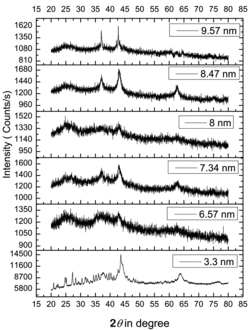
The results from the X-ray investigations of some of the samples are presented in . The observed diffraction peaks are in good agreement with the standard values (JCPDS no. 71-1179). All the samples exhibited the main peaks corresponding to (111), (200), (220), (311) and (222) planes of face-centred cubic (fcc) structure. No secondary phases were observed in the spectra of any of the samples, indicating that the synthesised samples are of high purity and contained no phases other than NiO. The lattice constant of bulk NiO is 4.195 Å whereas those of the samples synthesised in this work differed from this value on account of their nanocrystalline structure. From the XRD peakwidths, the average crystallite sizes of the different samples were estimated by using the Debye–Scherrer equation [Citation12] and they varied from 3.3 to 12.6 nm. The sample treatment temperature, the time of annealing, molarity of the precursor solution used and the obtained crystallite sizes are given in . From the table, it is clear that the particle size is very sensitive to the changes in any of these starting parameters although a systematic change of variation of any or all of these parameters often did not yield the same expected effect on the particle sizes. Still, it needs to be pointed out here that, in general, an increase in the size of the nanoparticles has been affected by an increase in any one or all the three of these parameters for bringing in the growth of nanoparticles.
Table 1. The sample treatment temperature, time of annealing, molarity of the precursor solution and the obtained crystallite sizes. Typical error in the estimation of particle sizes (from X-Ray Diffraction patterns) is 4.0%.
Figure 1. XRD patterns of a few NiO samples.
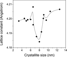
The lattice constants (a) of the different samples were estimated from the XRD data by combining the Bragg's equation with the crystallographic plane spacing (d) and getting the relation(1) shows the variation of the lattice constant (a) estimated from the above relation with crystallite size. The changes appear rather interesting as there is a definite lattice contraction with decreasing crystallite size initially but the trend then gets remarkably reversed as the average sizes of the crystallites are reduced further. The lattice constant is minimum for particles of diameters around 8 nm which is in the midway of the size range of particles studied in this work. More discussions are given afterwards.
Figure 2. The variation of the lattice constant (a) with crystallite size.
3.2. HRTEM studies
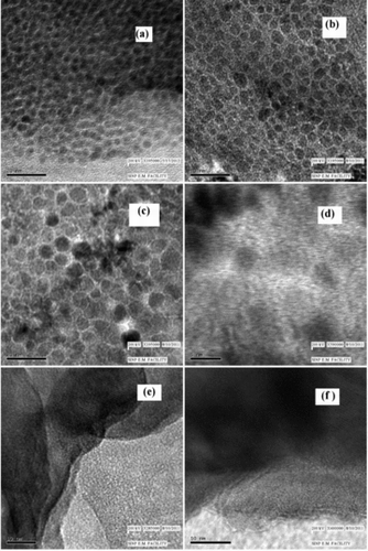
Some of the HRTEM images of NiO samples are shown in . The overview images ((a)–(c)) show that the samples entirely consist of NiO crystallites of sizes about 3.3, 6 and 8–9 nm, respectively, with larger particles or agglomerates being mostly absent. The images also show the hexagonal shape of the crystallites. Further, the well-developed lattice fringes shown in (d)–(f) demonstrate the high degree of crystallinity achieved during the synthesis of the samples. The spacing of the two neighbouring planes, for example, is about 0.24 nm in (d) and is consistent with the separation of the (111) planes in cubic (fcc) NiO.[Citation1]
Figure 3. HRTEM images of some of the NiO nanocrystalline samples: (a–c) the nanocrystalline particles and (d–f) the well-developed lattice fringes.
3.3. Optical absorption measurements
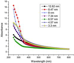
Ultraviolet (UV)–visible light absorption spectroscopy is one of the important methods to reveal the energy structures and optical properties of semiconductor nanocrystals. The optical absorption spectra in the range from 250 to 800 nm for the annealed nanocrystalline samples are presented in . It is evident that the absorption gradually decreases with an increase of the wavelength in the region from 380 to 800 nm.
Figure 4. (Colour online) Optical absorption spectra of the different samples.
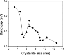
The optical bandgap Eg was calculated from the optical absorption spectra, using the well known relation αhν = A(hν − Eg)n where A is a constant, hν is the photon energy and n depends on the nature of transition. n is equal to 1/2 and 2 for direct and indirect transitions, respectively. It is well known that NiO nanoparticles are direct bandgap semiconductors. Hence, the optical bandgap for the annealed samples can be obtained by extrapolating the linear portion of the (αhν)2 vs. hν curve to zero. The bandgap of the NiO nanoparticles is found to be in the range of 4.02–4.26 eV (). Normally, the nanomaterials show a blue shift in the bandgap energy, but in the present work, we observed the blue shift in samples of relatively higher crystallite sizes, and a decrease in the bandgap value is additionally seen for samples having crystallites of sizes below 6.56 nm. Moreover, the bandgap again increases to 4.26 eV when the size of the crystallites decreased further below 5.33 nm. The values of Eg and its changes with the changes in particle sizes are typically identical in nature and magnitude to similar changes due to the occurrence of quantum confinement effects observed earlier in certain other nanomaterial systems.[Citation13,14] Especially, in semiconductor nanoparticles, such effects directly manifest as increases in bandgap energy (Eg), and the increase usually is of the order of 0.1–1.0 eV. This happens when the particle sizes are reduced to below the exciton Bohr diameter of the material, as explained later. The relation connecting the two is of the form given below [Citation15]:(2)
Figure 5. The bandgap estimated from the optical absorption spectra versus average particle sizes of the crystallites of the different samples.
3.4. Positron lifetime measurements
Typical peak-normalised positron lifetime spectra of a few selected samples are shown in . The extended multi-exponential nature of the row spectra itself signifies the presence of rich concentrations of vacancy-type defects in the samples used here. The detailed analysis carried out by the program PALSfit [Citation10] gave best fit (χ2/f = 1.0 ± 0.15, f is the degree of freedom) for three positron lifetime components, named as τ1, τ2 and τ3 in the ascending order of their magnitudes. The corresponding relative intensities are named as I1, I2 and I3 irrespective of their magnitudes. The values of these lifetimes and intensities are shown in and against the crystallite sizes of the corresponding samples. The longest of these lifetimes τ3 with intensity I3 () is related to the formation and subsequent annihilation of orthopositronium atoms (o-Ps), a metastable spin-triplet-bound state of the electron and positron and which is generally formed in sites of very low electron density. (The singlet state called parapositronium (p-Ps), where the spins of electron and positron are oriented in opposite directions, is also possible to form, but with a reduced probability Ip-Ps = I3/3. Since I3 itself in the present work is less than 1.2%, the presence of p-Ps is ignored.) Nanocrystalline materials are specially of attention due to the large network of crystallite boundaries and interfaces, and these are regions of low electron density owing to the deficiency of adequate number of atoms to complete the crystal structure. These regions are therefore favourable sites for the formation of positronium in significant numbers, and the ‘pick off’ annihilation process, involving the capture of the positron in o-Ps by an electron with opposite spin from the material, reduces the positron lifetimes to values around a few nanoseconds.[Citation25] From an established model that relates its value to the size of free volume defects in amorphous materials,[Citation26,27] one can estimate the sizes of these interfacial defects as of the order of 0.2–0.3 nm. In other words, the average separations of the crystallites in the samples are of this order.
Figure 6. (Colour online) Peak-normalised positron lifetime spectra of some of the NiO nanocrystalline samples.
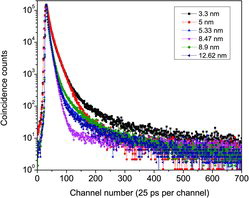
Figure 7. The variation in the positron lifetimes τ1 and τ2 and the relative intensity I2 versus the crystallite sizes of the NiO nanoparticles.
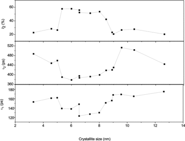
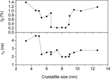
Figure 8. The ortho Ps lifetime τ3 and its intensity I3 versus the crystallite sizes of the NiO nanoparticles.
The magnitudes of the next longest positron lifetime component τ2 shown in are also very large when compared to the reported lifetime of τb = 110 ps in NiO [Citation28] and they indicate positron annihilation from very large vacancy clusters. Such magnitudes in coarse materials are normally attributed to voids and cavities. In nanocrystalline materials, since the particle sizes are rather small (less than 15 nm in this work), it is rather incomprehensible to have such large size defects within particles of ultrafine sizes. It is therefore reasonable to state that the very large values of τ2 are results of positrons annihilating from both within the defects in the nanoparticles as well as at the extended defects on the crystallite surfaces. It is to be noted that the thermalised positrons can diffuse through the material over distances typically of the order of a few tens of nanometers in oxide semiconductors, and hence, a fraction of positrons can always traverse through the material to the surfaces of the crystallites if the latter are of diameters less than the thermal diffusion length of positrons.[Citation29,30]
In the context of positron annihilation from the defects within the nanoparticles, it should be pointed out that the charge state of the vacancy cluster is a decisive factor, which needs to be discussed here. A cationic monovacancy, resulting due to the absence of a Ni2+ ion and denoted as VNi, is negatively charged and hence can attract positrons to it. On the other hand, anionic monovacancy caused by the absence of an O2− ion (VO) will have positive charge and repel the positron. A combination of the two will be a divacancy (VNi+O) and it will be electrically neutral. A neutral vacancy can also trap positrons since the absence of the positive nuclear charge offers an attractive site for positrons. Positron trapping in a trivacancy is selective for this reason, since such a defect cluster can be formed either by the combination of one cationic and two anionic vacancies (VO+Ni+O) or vice versa (VNi+O+Ni). The former has a resultant positive charge and hence positron trapping is ruled out. The latter has the potential to trap positrons and give them lifetimes large enough to reflect it as a distinctly resolvable component in the data analysis.
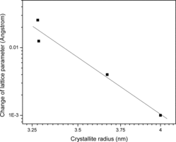
From the variation of the different positron annihilation parameters with change in average particle size, as illustrated in and , a striking observation is the drastic increase of the positron lifetimes, especially τ1 and τ2, at very low particle sizes. We had similar observations in a few earlier works too [Citation13,14] but the present one is remarkable. The intensity I2 of the component had fallen too, as if the effect is one of defect agglomeration. However, a more probable feature is the occurrence of quantum confinement effects, as discussed in the previous section. It is to be noted that the sharp decrease in the lattice parameters observed in samples of crystallite sizes below 9.0 nm () is a feature exhibited in the variations of the two lifetimes as well, and the intensity of the long-lived component I2 showed a substantial increase (). The decrease of lattice parameter can result from strain induced by the increasing number of surface atoms in an effort to minimise the surface free energy. Unlike in a bulk solid or coarse crystallite where the number of core atoms far outnumber the surface atoms and offer stiff resistance to surface reduction, the inner core of a nanoparticle is soft enough to contract in order to facilitate the minimisation of surface energy and this accounts for the reduction of positron lifetimes that starts taking place when the crystallite size is reduced below 9.0 nm. The sharp but uncharacteristic expansion of the lattice seen in particles below a size of 8 nm emerges from the influence of the strain caused by the crystalline defects. In a detailed discussion on the size-dependent lattice expansion in nanoparticles, Diehm et al. [Citation31] has pointed out about the role of point defects and the strain associated with them on changing the lattice parameters in metal oxide semiconductors. According to this study, if the lattice expansion is caused by the presence of the defects, a log–log plot of the change in lattice parameter versus particle size (radius R) should have a 1/R dependence. Incidentally, this has been found true in the present case too () and the lattice parameter has shown an increase when the particle sizes decreased below 8 nm (). Significantly, this effect is found prominent when the particle sizes are too low (<8 nm) and the two positron lifetimes and intensity remained saturated in this region. However, it should be seen that the lattice expansion ceases to be over (in the decreasing direction of the crystallite size) below 6 nm size of the crystallites whereas both the bandgap Eg () and the positron lifetimes τ1 and τ2 continue to rise (). The significant increase of the positron lifetimes incidentally coincides with the particle size below which strong quantum confinement effects were observed as depicted in . The increase in positron lifetimes due to quantum confinement effects needs to be understood as further explained later. No matter whether positrons get annihilated while in the Bloch state (reflected in τ1) or from the defects or surfaces (reflected in τ2), the overlap of the positron wavefunction with those of core electrons significantly reduces with increase of the bandgap and the probability of annihilation especially when the positrons are trapped in the defects also decreases. The positron lifetimes therefore increase and the intensity parameter I2 decreases.
Figure 9. The change in lattice parameter (Δa) versus the average crystallite radius in the NiO nanoparticles of size range 6.56–8 nm in a log–log scale.
The longest positron lifetime component τ3 and its intensity I3, as already stated, arise from ortho Ps atoms formed within the intercrystallite regions and as such do not bear any correlation in its variation with the decreasing sizes of the crystallites. Still, a systematic change can be observed occurring in their values in their variation with the crystallite size, as depicted in . For example, the effects of lattice contraction and subsequent expansion, which we had earlier observed in the variation of the other lifetimes τ1 and τ2 (), do not seem to have any influence on the variation of τ3 whereas I3 falls down in this region (between the crystallite sizes 8.9–8.0 nm). Similarly, the subsequent finite size effects are also reflected in their rises at smaller crystallite sizes.
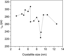
In an earlier experimental result reported by Kar et al. [Citation13] on CdS nanoparticles, the mean positron lifetime defined as(5) had been shown to increase remarkably with the reduction of crystallite sizes below the exciton Bohr diameter due to similar effects. As already explained, the positrons after entering a solid get rapidly (about in <10 ps) thermalised and hence will have high diffusivity through the solid until they meet with their eventual annihilation with electrons. A further consequence of such diffusion in nanocrystalline materials is that the positrons will diffuse out to the surfaces as the crystallite size is smaller than the positron diffusion length (∼50 nm [Citation29,30]). At the structural free volumes on the crystallite surfaces, the lifetime of the positrons is governed by the overlap of the positron wavefunction with the local electron density. With the increasing bandgap, this overlap is now gradually reduced resulting in an increase in the positron lifetime. The positron mean lifetime defined by Equation (5) reflects a cumulative effect of the annihilation of all the positrons entering the sample. In its variation with average crystallite size of the samples (), the occurrence of quantum size effects is clearly displayed, revealing the sensitivity of the PAS to such electronic structural changes.
Figure 10. The mean positron lifetime τm versus the crystallite sizes of the NiO nanoparticles.
3.5. Coincidence Doppler broadening measurements
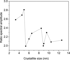
Following the detection of the two outgoing annihilation gamma-rays of energy E1 and E2, a two-parameter spectrum is generated by defining E1 + E2 and E1 − E2 in the coplanar perpendicular axes and counts distributed accordingly.[Citation32,33] The one-dimensional projection parallel to the energy-difference axis, integrated over E1 + E2 = 1.022 ± 0.0024 MeV, is a spectrum of high statistics and free of resolution and background effects. Still, to blow up the very small variations in the electron momentum distribution in the different samples, ratio curves have been generated by dividing the area-normalised spectra with that of a well-annealed iron sample. The results are illustrated in . A characteristic peak corresponding to pure Ni is observed in the case of all the other curves too at pL = 27.3 × 10⁻³ m0c. The observation is very significant if one looks from the point of view of the sensitivity of positrons to the charge states of the vacancies or their clusters.[Citation34,35] Normally, for being into the proximity of a Ni elemental environment, the positrons will have to reside in oxygen vacancies. This is, however, ruled out owing to their Coulomb repulsive interactions. The situation significantly changes if (and when) the potential positron trapping centres are vacancy clusters, either negatively charged or neutral. The large values of τ2 obtained in positron annihilation measurements also support the trapping and annihilation of positrons in large vacancy clusters. Theoretical studies are necessary to pinpoint their exact nature and composition (VmNi+nO, m and n are the number of cations and anions missing to form the vacancy cluster). In order to follow the small variations in the electron momentum distribution as scanned by the positrons, we have further plotted the amplitudes of the peaks (after area normalisation) against the crystallite sizes (), and the nature of variation strangely bears a striking resemblance with that of the mean positron lifetime shown in . It establishes the various processes like lattice contraction, followed by expansion and the stages of quantum confinement effects already discussed earlier. The absence of a characteristic peak at around 1.5 × 10⁻³ m0c originating from positron annihilation with 2p electrons of oxygen is perhaps due to the presence of oxygen layer at the surfaces of the reference iron sample used and which got divided when the ratio curves were generated.
Figure 11. (Colour online) CDBS ratio curves of a few selected samples together with an identical curve for pure and annealed Ni pellets with reference to the spectrum of well-annealed Fe pellets.
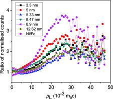
Figure 12. The amplitudes of the peak at pL = 27.3 × 10⁻³ m0c in the CDBS versus the crystallite sizes of the NiO nanoparticles.
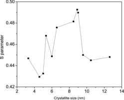
As yet another confirmation of the defect-related processes and finite size effects in the crystallites as their sizes are reduced, the Doppler broadened lineshape parameter S is plotted as a function of the crystallite size in . S has the usual definition as the quantity that represents the fraction of low momentum (free) electrons annihilated by positrons and hence sensitive to the vacancy-type defects within the material.[Citation25] It is derived from the one-dimensional projected spectra that we obtained in the CDBS analysis as the ratio of counts within the central segment E1 − E2 = 0 ± 2.4 keV to the total counts under the curve. shows characteristic stages of positron annihilation with electrons depicting processes related to their redistribution. For example, S increases in the initial stages of size reduction due to the increase in the surface to volume ratio that signifies the diffusion of more number of positrons to the crystallite surfaces. The subsequent lattice contraction is indicated by a gradual fall of it, although the intermittent expansion in the range 8.00–6.57 nm is surprisingly missing. Contrary to earlier findings,[Citation13] S did not change significantly at the onset of quantum confinement effects although an indication to this is seen at the smallest crystallite size (3.3 nm) used here. Perhaps, the variation of S can be strongly influenced by the positronium component that too undergoes variations in its lifetime and intensity, as illustrated earlier in .
Figure 13. The S parameter versus the crystallite sizes of the NiO nanoparticles.
4. Summary and conclusions
This paper has as its contents the detailed results of investigation of the structure and certain physical properties of NiO nanoparticles synthesized through chemical processes. From the synthesis point of view, it should be mentioned that the samples were obtained in sufficient degree of purity and narrow distribution of sizes in the nanometre range 3–13 nm. The samples were produced in a form compatible with the use of several experimental characterisation tools that proved their phase purity and stability. Subsequent investigation to study their optical properties revealed a significant increase in the bandgap energy that notified the occurrence of quantum confinement effects in the particles of very low sizes, especially below 6.56 nm. Interestingly, it manifested in two distinct stages, weak and strong confinement effects interspersed in between by a lattice contraction. Very encouragingly, PAS which has been popular otherwise only as a defect investigational probe is found to be very sensitive to these effects since a remarkable rise in the positron lifetimes is noticed at these stages. The other accompanying processes such as lattice contraction and then expansion as the crystallite sizes are reduced were also reflected. Although this work had confined itself into a very narrow range of crystallite sizes, the range chosen had been very special as it coincided with the range of quantum confinement in NiO. The study assumes significance from two aspects, first being a rarely reported one on NiO nanoparticles and second as a demonstration of the reliability of PAS for such investigations. It should be added that the crystallite sizes below which quantum confinement phenomenon set in were in agreement with the predictions based on theoretical evaluations of the finite size effects.
Acknowledgements
The authors thank the staff of the HRTEM facility of Saha Institute of Nuclear Physics, Kolkata for their help and cooperation. Authors also wish to thank Dr Goutam Das of National Metallurgical Laboratory, Jamshedpur and Dr Dipankar Das of University Grants Commission Consortium for Scientific Research, Kolkata for the X-ray diffraction measurements.
References
- Kalam A, Al-Sehemi AG, Al-Shihri AS, Du G, Ahmad T. Synthesis and characterization of NiO nanoparticles by thermal decomposition of nickel linoleate and their optical properties. Mater Characterization. 2012;68:77–81.
- Anandan K, Rajendran V. Morphological and size effects of NiO nanoparticles via solvothermal process and their optical properties. Mater Sci Semiconductor Process. 2011;14:43–47.
- Rao CNR, Raveau B. Transition metal oxides: structure, properties, and synthesis of ceramic oxides. 2nd ed. New York (Somerset, NY): Wiley; 1998. p. 1–392.
- Srivastava AK, Thota S, Kumar J. Preparation, microstructure and optical absorption behaviour of NiO thin films. J Nanosci Nanotechnol. 2008;8:4111–4115.
- Shah MA. A versatile route for the synthesis of nickel oxide nanostructures without organics at low temperature. Nanoscale Res Lett. 2008;3:255–259.
- Wu Y, He Y, Wu T, Chen T, Wan H. Influence of some parameters on the synthesis of nanosized NiO material by modified sol–gel method. Mater Lett. 2007;61:3174–3178.
- Han DY, Yang HY, Shen CB, Zhou X, Wang FH. Synthesis and size control of NiO nanoparticles by water-in-oil microemulsion. Powder Technol. 2004;147:113–116.
- Li X, Zhang X, Li Z, Qian Y. Synthesis and characteristics of NiO nanoparticles by thermal decomposition of nickel dimethylglyoximate rods. Solid State Commun. 2006;137:581–584.
- Wu M-S, Hsieh H-H. Nickel oxide/hydroxide nanoplatelets synthesized by chemical precipitation for electrochemical capacitors. Electrochim Acta. 2008;53:3427–3435.
- Olsen JV, Kirkegaard P, Pedersen NJ, Eldrup M. PALSfit: a new program for the evaluation of positron lifetime spectra. Phys Status Solidi C. 2007;4:4004–4006.
- Chatterjee A, Ramachandran K, Kumar A, Behere A. Linux Advanced MultiParameter System. Trombay, Mumbai (India): Nuclear Physics Division, BARC; 2013. Available from: http://www.tifr.res.in/~pell/lamps.html
- Cullity BD. Elements of X-ray diffraction. Reading (MA): Addison-Wesley; 1956. p. 167–171.
- Kar S, Biswas S, Chaudhuri S, Nambissan PMG. Finite-size effects on band structure of CdS nanocrystallites studied by positron annihilation. Phys Rev B. 2005;72:075338.
- Das S, Ghoshal T, Nambissan PMG. Positron annihilation studies of NiO nanoparticles prepared through two different chemical routes. Phys Status Solidi C. 2009;6:2569–2571.
- Brus LE. A simple model for the ionization potential, electron affinity, and aqueous redox potentials of small semiconductor crystallites. J Chem Phys. 1983;79:5566–5571.
- Choi SC, Koumoto K, Yanagida H. Electrical conduction and effective mass of a hole in single-crystal NiO. J Mater Sci. 1986;21:1947–1950.
- Michael DI, Servaites JD, Buchholz DB, Leever BJ, Liu J, Emery JD, Zhang M, Song J-H, Durstock MF, Freeman AJ, Bedzyk MJ, Hersam MC, Chang RPH, Ratner MA, Marks TJ. Structural and electrical functionality of NiO interfacial films in bulk heterojunction organic solar cells. Chem Mater. 2011;23:2218–2226.
- Roy B, Chakravorty D. Anomalous resistance change in nanocrystalline metallic systems. Solid State Commun. 1993;87:71–75.
- Nanda J, Kuruvilla BA, Sarma DD. Photoelectron spectroscopic study of CdS nanocrystallites. Phys Rev B. 1999;59:7473–7479.
- Fernández-Garcia M, Rodriguez JA. In:Lukehart CM, Scott RA, editors. Nanomaterials: inorganic and bioinorganic perspectives. New York (NY): Wiley; 2008. p. 453–512.
- Rao KV, Smakula A. Dielectric properties of cobalt oxide, nickel oxide, and heir mixed crystals. J Appl Phys. 1965;36:2031–2038.
- Wood DM, Ashcroft NW. Quantum size effects in the optical properties of small metallic particles. Phys Rev B. 1982;25:6255–6274.
- Michael DI, Buchholz DB, Hains AW, Chang RPH, Marks TJ. p-type semiconducting nickel oxide as an efficiency-enhancing anode interfacial layer in polymer bulk-heterojunction solar cells. Proc Natl Acad Sci USA. 2008;105:2783–2787.
- Moriyasu K, Osako S, Mori N, Hamaguchi C. Effect of quantum confinement and lattice relaxation on electronic states in GaAs/In0.2Ga0.8As/GaAs quantum dots. Jpn J Appl Phys. 1997;36:3932–3935.
- Siegel RW. Positron annihilation spectroscopy. Annu Rev Mater Sci. 1980;10:393–425.
- Tao SJ. Positronium annihilation in molecular substances. J Chem Phys. 1972;56:5499–5510.
- Eldrup M, Lightbody D, Sherwood JN. The temperature dependence of positron lifetimes in solid pivalic acid. Chem Phys. 1981;63:51–58.
- Barbiellinii B, Genoud P, Jarlborg T. Calculation of positron lifetimes in bulk materials. J Phys. 1991;3:7631–7640.
- Zhang Y, Ma X, Chen P, Li D, Pi X, Yang D, Coleman PG. Enhancement of electroluminescence from TiO2/p+-Si heterostructure-based devices through engineering of oxygen vacancies in TiO2. Appl Phys Lett. 2009;95:252102.
- Zubiaga A, Tuomisto F, Plazaola F, Saarinen K, Garcia JA, Rommeluere JF, Zuniga-Perez J, Munoz-Sanjose V. Zinc vacancies in the heteroepitaxy of ZnO on sapphire: influence of the substrate orientation and layer thickness. Appl Phys Lett. 2005;86:042103.
- Diehm PM, Ágoston P, Albe K. Size-dependent lattice expansion in nanoparticles: reality or anomaly? ChemPhysChem. 2012;13:2443–2454.
- Asoka-Kumar P, Alatalo M, Ghosh VJ, Kruseman AC, Nielsen B, Lynn KG. Increased elemental specificity of positron annihilation spectra. Phys Rev Lett. 1996;77:2097–2100.
- Nagai Y, Nonaka T, Hasegawa M, Kobayashi Y, Wang CL, Zheng W, Zhang C. Direct evidence of positron trapping at polar groups in a polymer-blend system. Phys Rev B. 1999;60:11863–11866.
- Krause-Rehberg R, Leipner HS. Positron annihilation in semiconductors – defect studies. Berlin: Springer; 1999. p. 1–379.
- Ghoshal T, Kar S, Biswas S, De SK, Nambissan PMG. Vacancy-type defects and their evolution under Mn substitution in single crystalline ZnO nanocones studied by positron annihilation. J Phys Chem C. 2009;113:3419–3425.