
Abstract
Electrospun ZnO nanofibres with a diameter in the range of 74–125 nm were synthesised by optimising various parameters. Zinc acetate was used as a precursor and optimised to obtain a homogeneous and interconnected porous ZnO nanofibres network. The ZnO/poly(vinylpyrrolidone) composite nanofibres were calcined at 450 °C for 2.5 h to obtain continuous nanofibres network. The morphology of the nanofibres was studied by scanning electron microscopy and imageJ software. The structural and optical properties of the synthesised nanofibres were studied by surface profiler, X-ray diffraction and ultraviolet–visible spectroscopy. The grain size increased while the bandgap was observed to decrease with increased precursor concentration. The effect of precursor concentration was also studied to improve the power conversion efficiency of ZnO nanofibres/poly(3-hexylthiophene) (P3HT): [6,6]-phenyl C61-butyric acid methyl ester (PCBM) photovoltaic device. The efficiency was improved from 0.896 ± 0.007% to 2.29 ± 0.03% by introducing the electrospun ZnO nanofibres.
1. Introduction
One-dimensional (1D) nanostructures such as nanofibres,[Citation1,2] nanotubes,[Citation3,4] nanorods,[Citation5,6] beaded nanochains,[Citation7] template-directed mesoporous structure [Citation8] and nanowires [Citation9,10] are the focus of research during recent years due to their excellent properties as demanded by novel applications. There are various techniques for synthesising these structures. The most recent reported techniques are electrospinning (ES),[Citation11,12] hydrothermal,[Citation13,14] chemical vapour deposition (CVD) [Citation15] and solvothermal.[Citation16] Among all these and many more available methods for producing nanostructures, ES is a low-cost, convenient technique for the fabrication of metal oxide nanofibres. The advantage of this technique is to obtain continuous length nanofibres with uniform and controllable diameter.
There are various reports where electrospun nanofibres were fabricated [Citation17,18] and their structural properties were analysed. It is of more importance to analyse both the structural and optical properties of ZnO nanofibres for optoelectronic devices, particularly for photovoltaic (PV) applications. To the best of our knowledge, there are no reports where such properties of the ZnO nanofibres were investigated by variation in precursor concentration to study solar devices.
The nanofibrous network having forementioned structural properties is much demanded by various applications, especially by the PV devices. The 1D nanostructures of ZnO have also diverse properties such as high carrier mobility, direct wide bandgap and are most importantly environment friendly. Therefore, they are promising candidate for application in optoelectronic devices, sensors and transducers. The challenge in organic PV (OPV) devices is the low-power conversion efficiency (PCE), which can be overcome by introducing low-cost and high-mobility metal oxide ZnO nanostructure. There are some structural properties such as small diameter and high surface to volume ratio of metal oxide nanostructures, which are helpful to improve the PCE of PV devices. There are various attempts where nanostructures were used to improve the PCE. The introduction of ZnO nanowires was reported to improve device efficiency up to 0.53%.[Citation19] ZnO nanofibres/P3HT PV device having 0.53% maximum efficiency was reported by using vertically oriented ZnO nanofibres.[Citation20] The influence of ZnO nanorods length was studied to improve fill factor (FF) of P3HT:PCBM/ZnO nanorod PV devices.[Citation21] There was only a single report where electrospun ZnO nanofibres were reported to improve PCE of P3HT/electrospun ZnO nanofibres hybrid devices,[Citation22] where a maximum efficiency of 0.51% was achieved. In a recent report, we have studied the effect of polymer infiltration to improve the efficiency of ZnO nanofibres/P3HT:PCBM device and achieved a PCE of 2.23%.[Citation23] There are various challenges for this device structure to get an efficient device. One of them is to get small-diameter nanofibres having a long length without discontinuity and well interconnection. These parameters of the nanofibres control the resistance at the interface between the blend and nanofibres network. By considering these challenges along with other optimum device fabrication parameters, however, we were able to improve further the PCE of P3HT:PCBM bulk heterojunction device by incorporating ZnO nanofibres network.
In this study, first the synthesis of small-diameter nanofibres network by optimising the precursor concentration is reported. Second, the structural and optical properties of the synthesised nanofibres are presented, and third it is demonstrated that the application of interconnected diffused nanofibres network to P3HT:PCBM blended bulk heterojunction devices improves their efficiency.
2. Materials and methods
2.1. Synthesis of nanofibres
A sol with three different precursor concentrations was prepared by a reported method [Citation22] in two steps. The first step involved the dissolving of three distinct concentrations (0.15, 0.20 and 0.25 g) of zinc acetate (ZnAc) and poly(vinylpyrrolidone) (PVP) (MW 40,000) (0.3 g) in a mixture of 2-methoxyethanol (3 ml) and ethanolamine (0.05 ml). The homogeneous gel was obtained after a second step by the addition of isopropanol (1.5 ml) and continuous stirring for ∼14 h at room temperature. The chemicals used in this study were purchased from Sigma Aldrich. Each of the three gels was loaded for ES in a plastic syringe attached to a stainless steel needle. The various parameters like distance between the needle tip and collector plate (10 cm), applied voltage (7.5–8.0 kV), flow rate (0.30–0.35 ml/h) and ES time (5 min) was optimised to obtain continuous long-length nanofibres. It is very important to have a homogeneous nanofibre film well adhered to the substrate, which is a difficult task. This challenge was overcome by spin coating an adhesive layer of a solution having an optimum viscosity to have a minimum contact angle with the substrate. Prior to this layer, three indium-doped tin oxide (ITO) coated glass slides were cleaned by cyclohexane, chloroform, acetone and de-ionised water and dried with the nitrogen gas. The process was followed by spin coating an adhesive layer (30 ± 10 nm) of a solution containing ZnAc (0.2 g) dissolved in 5 ml of 2-aminoethanol at 5000 rpm for 30 s and annealing at 475 °C for 15 min. The first sample was electrospun by a gel containing 0.15 g of ZnAc and labelled as ‘S1’. The second and third were electrospun by the gel having 0.20 and 0.25 g of ZnAc and referred as ‘S2’ and ‘S3’, respectively. The electrospun nanofibres were kept for more than 12 h at room temperature in a low-moisture environment. The electrospun ZnO/PVP composite nanofibres were then calcined in air at an optimum calcination temperature (500 °C) and time (1 h) to obtain diffused interconnected polycrystalline ZnO nanofibres network.
2.2. Fabrication of photovoltaic devices
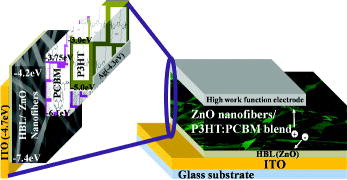
The effect of ZnO nanofibres applied to P3HT:PCBM blended bulk heterojunction devices was studied by incorporating three different structures. Each of the devices was fabricated by spin coating a homogeneous blend of P3HT (Rieke Metals, regioregularity 93%, MW 48,000) and PCBM (20:16) dissolved in chlorobenzene (1 ml). The schematics and the energy-band diagram of the materials used to fabricate the devices are shown in . The detailed structure of each device is given in the following. The first device ‘C1’ was fabricated by spin coating P3HT:PCBM blend on adhesive layer, which also acts as a hole-blocking layer (HBL). The other three devices ‘C2, C3 and C4’ were fabricated by spin coating P3HT:PCBM blend on electrospun substrates S1, S2, and S3, respectively. All the devices were pre-annealed on a hot plate at 110 °C for 15 min to enhance the infiltration of polymer through the pores of ZnO nanofibrous network. The top contact of Ag (100 nm) was thermally evaporated under vacuum of 10−6 mbar and then post annealed at 90 °C for 10 min in a nitrogen-filled glove box.
Figure 1. (Colour online) The energy-level illustration of the materials used (left) and schematics of ITO/HBL/ZnO nanofibres/P3HT:PCBM/Ag photovoltaic fabricated device (right).
The morphology and diameter of electrospun nanofibres were studied by Hitachi S-4700 scanning electron microscopy (FE-SEM) and ImageJ software. The structural properties were analysed by Rigaku diffractometer using CuKα (λ = 1.54059 Å. The thickness of the electrospun nanofibres and the fabricated device layers was analysed by using surface profiler surfcorder ET3000. Ultraviolet–visible (UV-vis) spectroscopy was carried out on Perkin Elmer Lambda. The performance of the fabricated devices was calculated by using Keithley 236 under illumination of 100 mw/cm2 (Solar simulator Newport 69911equipped with an AM1.5 filter).
3. Results and discussion
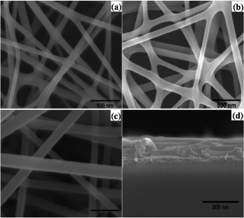
The morphology of the electrospun ZnO nanofibres is shown by SEM images in . The diameter of the nanofibres depends upon the concentration of ZnAc in the precursor solution used for ES as summarised in , the minimum diameter (74 ± 17 nm) nanofibres were synthesised when the ES gel had 0.15 g of ZnAc. The diameter of the nanofibres can further be reduced by decreasing the ZnAc concentration. However, small-diameter and continuous nanofibres are the best candidates for application to efficient PV devices, but the challenge is to obtain nanofibres having both the mentioned characteristics. It was found that by decreasing the concentration of ZnAc below 0.15 g, the fibres started melting at even low calcination temperature, so with this concentration a diffused interconnected nanofibres network was achieved as shown in (a) and (d). Therefore, there is a lower limit of ZnAc concentration for obtaining long-length diffused nanofibres. On the other hand, the diameter of nanofibres becomes large (125 ± 22 nm) as the concentration of ZnAc has increased to 0.25 g as shown in (c), which is not supposed to be good for efficient PV devices. The large diameter of the nanofibres imposes the upper limit on increased ZnAc concentration in the precursor gel, while decomposition of nanofibres restricts the further reduction in ZnAc concentration. The thickness of the nanofibres film recorded by surface profiler was 181 ± 17, 202 ± 13 and 217 ± 21 nm for the samples S1, S2 and S3, respectively, which indicated an increase with increase in the precursor concentration.
Table 1 The detail of the samples by precursor concentration and diameter of resultant calcined electrospun ZnO nanofibres with crystallite size and bandgap variation.
Figure 2. SEM images of: (a) sample S1 electrospun by sol–gel containing 0.15 g ZnAc; (b) sample S2 having 0.20 g precursor concentration; (c) sample S3 electrospun by sol–gel containing maximum precursor concentration and (d) cross-section of the electrospun ZnO nanofibres on an ITO/HBL coated glass substrate.
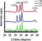
The X-ray diffraction (XRD) pattern of the synthesised ZnO nanofibres with different precursor concentrations is shown in . The diffraction peaks from the plane (100), (002), (101) and (102) were observed for all the samples, confirming the structure is wurtzite. The most prominent orientation in all the film was along (101) plane. The crystallite size (D) for this plane is indicated in for each sample and was calculated by using Scherer equation,[Citation24] D = 0.9λ/βcosθ, where λ is the wavelength of the X-ray radiation used, β is the full width at half maximum (FWHM) in radians and θ is the diffraction angle. The XRD patterns show that there is a decrease in the intensity of the Bragg peaks with the increase in ZnAc concentration, which could be due to better crystallisation of the nanofibres with change in diameter.[Citation25] The smaller FWHM means better crystallisation, as intensity represents the orientation of plane. The larger D and smaller FWHM values for S3 indicate better crystallisation of the film with higher ZnAc concentration for which film thickness has also increased.[Citation26]
Figure 3. XRD pattern of the electrospun with different precursor concentrations and calcined at 500 °C for 1 h.
The UV-vis absorption spectrum was used to study the optical properties of the synthesised nanofibres. The direct energy bandgap (Eg) of the synthesised nanofibres was estimated by Tauc plot as shown in the inset of using Tauc equation [Citation27]; αhν = B(hν−Eg)2, where B is constant, α is absorption coefficient and is calculated by the equation [Citation28]; α = 2.303(A/t), where A is absorbance and t denotes the thickness of the film. The increase in absorption for sample S3 as shown in is the evidence of increased film thickness. The calculated bandgap was observed to increase with the decrease in crystallite size as indicated in and is in agreement with an earlier study.[Citation29] The bandgap has increased with decreased nanofibres diameter due to quantum confinement effect. The devices fabricated were characterised under 1.5 G solar simulator, and J–V curve of each of the devices is shown in . The performance of the devices is summarised in and the dependence of various device parameters on ZnAc concentration is shown in . The FF of the device without nanofibres is 49.2% and decreased to 42.1% for the device fabricated by using the sample S2. However, in this study, the FF starts increasing ((a)) for the devices having nanofibres of the largest diameter. The variation in the FF can be attributed to blend morphology and incorporation of ZnO nanofibres.[Citation20]
Table 2. Performance of P3HT:PCBM-based fabricated devices, without and with ZnO nanofibres under 1.5 G sun simulator.
Figure 4. UV-vis absorption spectrum of the three samples S1, S2 and S3 electrospun by sol–gel containing different ZnAc concentrations. The inset is the plots of (αhν)2 vs. photon energy of all the three samples.
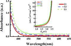
Figure 5. J–V curve of the four fabricated devices under 1.5 G sun simulator.
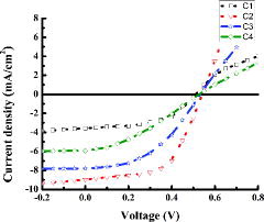
Figure 6. Dependence of various parameters of the fabricated devices upon precursor (ZnAc) concentration in the sol–gel used to electrospun ZnO nanofibres. (a) Fill factor dependence on ZnAc, (b) short circuit current density vs. ZnAc, (c) open circuit voltage as a function of ZnAc and (d) variation in power conversion efficiency with ZnAc.
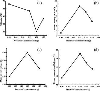
Short circuit current density (Jsc) is maximum (8.981 mA/cm2) for the devices fabricated with the smallest diameter nanofibres (S1), which might be due to the increased carrier generation by maximised exciton dissociation as shown in (b). The Jsc starts decreasing for the devices (C3 and C4) fabricated by relatively large-diameter nanofibres (S2 and S3). Another possible reason of increased Jsc is an injection of electron from P3HT:PCBM blend into ZnO nanofibres due to the suitable lowest unoccupied molecular orbital (LUMO) levels [Citation19] as indicated in . The pore size in the nanofibres network depends upon the diameter of nanofibres, so for small diameter nanofibres the pores are small, which help exciton dissociation at polymer/ZnO nanofibres interface, and more carriers are collected before recombination at the electrode. On the other hand, the pores are comparatively large for nanofibrous network obtained for larger diameter nanofibres and, therefore, exciton dissociation is reduced due to larger path length, so polymer blend infiltrated contribute less carriers. The interface between the small-diameter nanofibres (C2) and the polymer blend is close to the ideal length for exciton dissociation, so a major contribution in Jsc is observed for device C2.
The device C2 achieved maximum open circuit voltage (Voc) due to the fact that nanofibres have a range of Fermi-level position,[Citation30] therefore, Voc has increased for the devices fabricated by nanofibres.
The maximum PCE achieved (2.29 ± 0.03%) for the device (C2) fabricated with ZnO nanofibres electrospun from the optimum ZnAc concentration gel is more than twice of PCE achieved (0.896 ± 0.007%) by the device (C1) without nanofibres. It can be noted from that the major contribution toward maximum PCE is by Jsc due to the small diameter of nanofibres, as the diameter of ZnO nanofibres in this case is of the order of loosely bound exciton in inorganic nanostructure.[Citation31] The polymer has low mobility and ZnO nanofibres have high mobility,[Citation32,33] and the density of small-diameter nanofibres in the device C2 is higher as compared to large-diameter nanofibres in the device C4, so the same volume of the devices has a different polymer blend and nanofibres interface length, which might be the reason of higher PCE for the device C2. The UV-vis spectrum () indicates that the absorption is higher for the sample (S3) used for fabrication of the device C4 as compared to the sample (S1) used for device C2. This reduces the light absorption by P3HT:PCBM blend for device C4, which has low PCE. The introduction of nanofibres enhanced the carrier lifetime by quick charge transfer from LUMO of the P3HT:PCBM blend to the conduction band of ZnO nanofibres (high mobility) and then to ITO.[Citation34] The incorporation of ZnO nanofibres results in low series resistance of the device due to high mobility.[Citation35] Therefore, the PCE of the devices fabricated with ZnO nanofibres (C2, C3 and C4) is higher compared to the device (C1) without nanofibres.
4. Conclusions
Electrospun ZnO nanofibres were synthesised by optimising the precursor (ZnAc) concentration of the sol to obtain small-diameter, long-length, diffused and interconnected nanofibres. The minimum diameter of the nanofibres obtained was 74 ± 17 nm. The structural and optical properties showed that the grain size (7.64–15.72 nm) and the bandgap (3.29–3.20 eV) are controlled by the precursor concentration. The effect of precursor concentration (diameter of nanofibres) was studied to improve the PCE of ZnO nanofibres/P3HT:PCBM PV devices, and it was concluded that small-diameter nanofibres-based device can achieve a higher PCE (2.29 ± 0.03%).
Acknowledgements
The authors acknowledge the financial support by Higher Education Commission (HEC), Pakistan for this particular work. We are thankful to Gwangju Institute of Science and Technology, Korea for their support in characterisation during the study.
References
- Yu W, Jorge JS-A. Synthesis of lead zirconate titanate nanofibres and the Fourier-transform infrared characterization of their metallo-organic decomposition process. Nanotechnology. 2004;15:32–36.
- Xiong C, Balkus KJ Jr. Fabrication of TiO2 nanofibers from a mesoporous silica film. Chem Mater. 2005;17:5136–5140.
- Du G, Chen Q, Che R, Yuan Z, Peng LM. Preparation and structure analysis of titanium oxide nanotubes. Appl Phys Lett. 2001;79:3702–3704.
- Li W, Xie S, Qian LX, Chang B, Zou B, Zhou W, Zhao R, Wang G. Large-scale synthesis of aligned carbon nanotubes. Science. 1996;274:1701–1703.
- Dai H, Wong EW, Lu YZ, Fan S, Lieber CM. Synthesis and characterization of carbide nanorods. Nature. 1995;375:769–772.
- Wu JJ, Liu SC. Low-temperature growth of well-aligned ZnO nanorods by chemical vapor deposition. Adv Mater. 2002;14:215–218.
- Dutta M, Basak D. A novel and simple method to grow beaded nanochains of ZnO with superior photocatalytic activity. Nanotechnology. 2009;20:475602–475608. doi:10.1088/0957-4484/20/47/475602
- Chandra D, Mridha S, Basak D, Bhaumik A. Template directed synthesis of mesoporous ZnO having high porosity and enhanced optoelectronic properties. Chem Commun. 2009;6:2384–2386.
- Huang MH, Wu Y, Feick H, Tran N, Weber E, Yang P. Catalytic growth of zinc oxide nanowires by vapor transport. Adv Mater. 2001;13:113–116.
- Morales AM, Lieber CM. A laser ablation method for the synthesis of crystalline semiconductor nanowires. Science. 1998;279:208–211.
- Ma G, Fang D, Liu Y, Zhu X, Nie J. Electrospun sodium alginate/poly(ethylene oxide) core–shell nanofibers scaffolds potential for tissue engineering applications. Carbohydr Polym. 2012;87:737–743.
- Kim CH, Kim BH, Yang KS. TiO2 nanoparticles loaded on graphene/carbon composite nanofibers by electrospinning for increased photocatalysis. Carbon. 2012;50:2472–2481.
- Cao CL, Hu CG, Shen WD, Wang SX, Tian YS, Wang X. Synthesis and characterization of TiO2/CdS core-shell nanorod arrays and their photoelectrochemical property. J Alloys Compound. 2012;523:139–145.
- Xu CK, Gao D. Two-stage hydrothermal growth of long ZnO nanowires for efficient TiO2 nanotube-based dye-sensitized solar cells. J Phys Chem C. 2012;116:7236–7241.
- Gu XQ, Qiang YH, Zhao YL. Synthesis, structural and electrical properties of SiC nanowires via a simple CVD method. J Mater Sci Mater Electron. 2012;23:1037–1040.
- Ye N, Chen CC. Investigation of ZnO nanorods synthesized by a solvothermal method, using Al-doped ZnO seed films. Opt Mater. 2012;34:753–756.
- Wu H, Pan W. Preparation of zinc oxide nanofibers by electrospinning. J Am Ceram Soc. 2006;89:699–701.
- Yang X, Shao C, Guan H, Li X, Gong J. Preparation and characterization of ZnO nanofibers by using electrospun PVA/zinc acetate composite fiber as precursor. Inorg Chem Commun. 2004;7:176–178.
- Liu J, Wang S, Bian Z, Shan M, Huang C. Organic/inorganic hybrid solar cells with vertically oriented ZnO nanowires. Appl Phys Lett. 2009;94:173107–173103.
- Olson DC, Piris J, Collins RT, Shaheen SE, Ginley DS. Hybrid photovoltaic devices of polymer and ZnO nanofiber composites. Thin Solid Films. 2006;496:26–29.
- Takanezawa K, Hirota K, Wei Q-S, Tajima K, Hashimoto K. Efficient charge collection with ZnO nanorod array in hybrid photovoltaic devices. J Phys Chem C. 2007;111:7218–7223.
- Wu SJ, Tai QD, Yan F. Hybrid photovoltaic devices based on poly (3-hexylthiophene) and ordered electrospun ZnO nanofibers. J Phys Chem C. 2010;114:6197–6200.
- Tanveer M, Habib A, Khan MB. Improved efficiency of organic/inorganic photovoltaic devices by electrospun ZnO nanofibers. Mater Sci Eng B. 2012;177:1144–1148.
- Cullity BD, Stock SR. Elements of X-ray diffraction. Upper Saddle River (NJ): Prentice Hall; 2001.
- Ren H, Ding Y, Jiang Y, Xu F, Long Z, Zhang P. Synthesis and properties of ZnO nanofibers prepared by electrospinning. J Sol-Gel Sci Technol. 2009;52:287–290.
- Mohammed MA. Correlation between thickness, grain size and optical band gap of CdI2 film. Eng Techol J. 2009;27:1174–1183.
- Tauc J, editor. Amorphous and liquid semiconductors. London: Springer; 1974.
- Saleh WR, Saeed NM, Twej WA, Alwan M. Synthesis of sol-gel derived highly transparent ZnO thin films for optoelectronic applications. Adv Mater Phys Chem. 2012;2:11–16.
- Tan S, Chen B, Sun X, Fan W, Kwok H, Zhang X, Chua S. Blueshift of optical band gap in ZnO thin films grown by metal-organic chemical-vapor deposition. J Appl Phys. 2005;98:013505.
- Olson DC, Lee Y-J, White MS, Kopidakis N, Shaheen SE, Ginley DS, Voigt JA, Hsu JWP. Effect of ZnO processing on the photovoltage of ZnO/poly(3-hexylthiophene) solar cells. J Phys Chem C. 2008;112:9544–9547.
- Agranovich VM, Gartstein YN, Litinskaya M. Hybrid resonant organic–inorganic nanostructures for optoelectronic applications. Chem Rev. 2011;111:5179–5214.
- Chen W-B, Xiang H-F, Xu Z-X, Yan B-P, Roy VAL, Che C-M, Lai P-T. Improving efficiency of organic photovoltaic cells with pentacene-doped CuPc layer. Appl. Phys. Lett. 2007;91:191109–191103.
- Zhang ZY, Jin CH, Liang XL, Chen Q, Peng LM. Current-voltage characteristics and parameter retrieval of semiconducting nanowires. Appl Phys Lett. 2006;88:073102–073103.
- Liu R, Ye H, Xiong X, Liu H. Fabrication of TiO2/ZnO composite nanofibers by electrospinning and their photocatalytic property. Mater Chem Phys. 2010;121:432–439.
- Shaheen Sean E. Organic-based photovoltaics: toward low-cost power generation. MRS Bulletin. 2005;30:10–19.