
 ?Mathematical formulae have been encoded as MathML and are displayed in this HTML version using MathJax in order to improve their display. Uncheck the box to turn MathJax off. This feature requires Javascript. Click on a formula to zoom.
ABSTRACT
Metal sulphide CuS and CdS nanoparticles capped with Cetyltrimethylammonium bromide (CTAB) were synthesized by hydrothermal method. Structural, morphological, chemical composition, optical and luminescent properties were evaluated by different analytical techniques. X-ray diffraction (XRD) analysis of the CTAB capped metal sulfide nanoparticles reveals the formation of hexagonal structure. High-resolution transmission electron microscopy (HRTEM) images show that the morphology of the capped copper sulphide samples consists of hexagonal structure and capped cadmium has spherical shape and also confirms the crystalline nature of the particles with distinct lattice fringes. In FTIR spectroscopy, the composition of the CTAB capped CuS and CdS nanoparticles have been confirmed. The analysis of photoluminescence (PL) and optical transition show a red shift due to the reduction of band gap energy and it is attributed to the low defects and high crystallinity. The optical studies indicate that CuS and CdS nanoparticles with CTAB can be suitable for optoelectronic devices and photovoltaic applications.
1. Introduction
Semiconductor materials have been widely investigated due to their distinctive properties [Citation1,Citation2]. Recent years have witnessed a greater interest in the area of metal sulphide semiconductors due to their interesting optical, electronic, luminescent, mechanical, quantum size effect and other important physical and chemical properties [Citation3]. The synthesis of binary metal sulphide nanoparticles has been focused on II-VI [Citation4] and I-VI [Citation5] compounds, such as chalcogenides of cadmium and copper, as well as ZnS, HgS and MnS, on which a considerable degree of control upon their size and shape, and hence tunability of their optical and electronic properties has been achieved [Citation6,Citation7]. These materials exhibit interesting properties for modern industrial applications. Among these materials, CdS and CuS are typical direct band gap semiconductors having a band gap of 2.4 eV and 2.5 eV respectively for the hexagonal wurtzite phase at room temperature. Specifically, these materials are excellent photocatalytic materials, sensitive to visible light and are widely used in field effect transistors, light-emitting diodes, electronics, photodiodes, solar cells, sensors, optical materials, various luminescence devices and so on [Citation4,Citation8]. It is found that the optical and optoelectronic properties of CdS and CuS nanoparticles largely depend on their size and morphology.
Herein, we report the CdS and CuS nanoparticles synthesized in aqueous media with cationic surfactant CTAB as passivating agent. The purpose of this paper is to explore the optical and PL properties of CdS and CuS nanoparticles during nucleation and growth in the presence of cationic surfactant that would be useful in understanding the origin of these properties. The reasons for this choice are as follows: (a) the surface of large CdS and CuS particles are negatively charged over a broad range of conditions and even down to quite low pH values. (b) Mehta and Sanjay [Citation9] reported that the surfactants with charges on their head group to behave as lewis acid or base towards the ZnS nanoparticles surface. CTAB plays an important role as a stabilizer in modification and creation of surface recombination centers which can significantly change the optical properties of metal sulphide nanoparticles [Citation10].(c) An important aspect of micellar medium is the ability to control the growth rate and prevents the self-aggregation of nanoparticles by capping the surface charge. However, 1) ligand control is not only on growth rate, but also the nucleation rate which is equally critical to final particle size [Citation11]. 2) The surface charging is not the only factor on the optical properties [Citation12]. A plethora of techniques including hydrothermal synthesis, chemical vapor deposition, electrochemical synthesis and solvothermal reaction have been exploited to prepare CdS and CuS in diverse appearances for various applications [Citation5,Citation8], among which the hydrothermal method is considered to be efficient, because it is demonstrated to be effective for controlling the shape and size of nanomaterials [Citation10]. The in-house prepared nanoparticles were characterized by X-ray diffraction (XRD) analysis, Transmission electron microscopy (TEM), Fourier transform infrared spectroscopy (FTIR), UV-visible spectroscopy and Photoluminescence spectroscopy.
2. Materials and methods
2.1 Materials
Cadmium acetate [Cd(CH3COO)2.H2O], Copper acetate [Cu(CH3COO)2.H2O], Sodium hydroxide (NaOH), Cetyltrimethylammonium bromide (CTAB) were purchased from Loba (India). Thiourea (CH4N2S) and ethanol were obtained from Merck (India). The chemicals were of analytical grade and were utilized without additional purification. Deionized water was used as a solvent for all the experimental process. The glasswares were properly washed and sanitized.
2.2 Synthesis of CTAB capped CdS and CuS nanoparticles
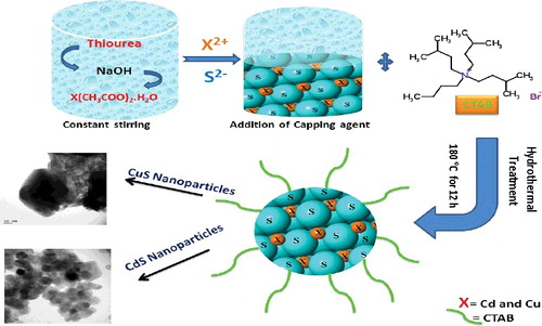
In a typical preparation process, Cadmium acetate, Copper acetate and Thiourea were used as precursors and NaOH as the mineralizer for the hydrothermal synthesis of CdS or CuS nanoparticles. The process began with dissolving Cadmium acetate or Copper acetate (0.2 M) and CH4N2S (0.5 M) into 20 mL of double distilled water separately to form two transparent solutions. There after 20 mL NaOH (1 M) solution was added little by little facilitated by magnetic stirring into the Cadmium acetate or Copper acetate transparent solution to maintain the pH around 8. Thiourea solution was added drop by drop into the above mixed solution under vigorous stirring using magnetic stirrer at room temperature and then CTAB (0.3 g) was added to this. Finally, the resulting solution was transferred into a 100 mL Teflon-lined stainless autoclave with a fill factor of approximately 70%. The autoclave was sealed and maintained in a furnace at 180 °C for 12 h. The autoclave was cooled naturally to room temperature. Thus, the uncapped yellow (greenish black) precipitate of CdS (CuS) was obtained and it was washed several times in double distilled water and ethanol by centrifugation and ultrasonication. Finally, the product was annealed in a furnace maintained at 150 °C for 10 h and used for further characterization. The annealing temperature was chosen considering the thermal steadiness of the compounds. The schematic diagram of the synthesis process is shown in .
Figure 1. Schematic illustration of formation pattern of CTAB capped CuS and CdS Nanoparticles.
2.3 Characterization
The structural characterization of the samples were recorded by powder X-ray diffraction patterns (XRD) using X-ray Diffractometer (X’ Pert PAN Analytical) with Cukα radiation (λ = 1.5406 Å) in 2θ ranging between 20° and 80°. The morphology and size were determined by the high-resolution transmission electron microscopy (HRTEM) and selected area electron diffraction (SAED) images were obtained on a microscope (JEOL, JEM-2100). TEM specimens were prepared by placing a few drops of liquid sample on a small copper grid and the sample was air dried at room temperature. The dried samples are investigated in the electron microscope. TEM images were operated at 200 kV acceleration voltages. FTIR spectra were recorded with KBr pellets on a Bruker Vector 22 FTIR spectrometer to identify the functional groups in the samples over the range of wave number 400–4000 cm−1. The UV-visible Diffuse Reflectance Spectral (UV-Vis/DRS) analyses were measured in the range of 200–1200 nm on a (JASCO-V-670) UV-visible Spectrophotometer. The photoluminescence (PL) measurements were performed on a LS 45 fluorescencespectrometer equipped with Xenon lamp as the excitation source.
3. Results and discussions
3.1 X-ray diffraction analysis
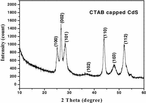
To ascertain the crystalline nature of CTAB capped CuS and CdS nanocrystalline powders were explored by X-ray diffraction patterns shown in and . The diffraction peaks were found to be sharp and intense which implies the high crystallinity of the samples. The pronounced diffraction peaks indexed can be assigned to the hexagonal wurtzite phase of CdS (JCPDs card no: 75–1545) [Citation11] and CuS (JCPDs card no: 06–0464) [Citation8] respectively. In , it is worth noting that the intensities of (103) and (006) diffraction peaks are lower than those of the standard patterns and however, the intensities of (110) diffraction peak in the XRD pattern was particularly strong, indicating the presence of preferential orientation in the sample [Citation13]. In , it can be noted that the (002) diffraction peak is comparatively strong and narrow, which can be ascribed to the preferential crystal growth orientation along the c-axis [Citation14].
Figure 2. X-ray diffraction pattern of as prepared CTAB capped CuS nanoparticles.
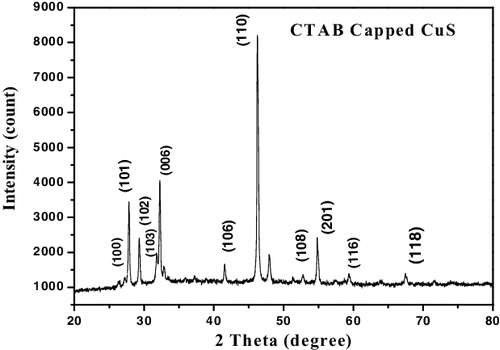
Figure 3. X-ray diffraction pattern of as prepared CTAB capped CdS nanoparticles.
The crystallite size (Φ) was estimated from the highest intense peak (110) for CuS and (002) for CdS using Sherrer EquationEquation (1)(1)
(1) :
(1)
(1)
Where, k is the proportionality constant (k = 0.89), λ is the wavelength of the Cu kα X-rays (1.5405 Å), βhkl is the full width at half maximum (FWHM) of the diffraction peak in radians and θ is the diffraction angle in degrees [Citation15]. According to the calculation, the crystallite size of CTAB capped CuS and CdS was found to be 32 and 12 nm respectively. The lattice parameters a and c, tabulated in , were calculated from the interplanar spacing of different (hkl) planes using the following EquationEquation (2)(2)
(2) [Citation15].
(2)
(2)
Table 1. Calculated crystallite size (Φ), lattice parameters (a and c), volume (V) of unit cell, internal local strain (ϵ) and average crystallite sizes obtained from the Sherrer, Williamson-Hall and HRTEM analysis of CTAB Capped CuS and CdS Nanoparticles
The volume (V) of the unit cell for the hexagonal system was calculated using EquationEquation (3)(3)
(3) . [Citation15].
(3)
(3)
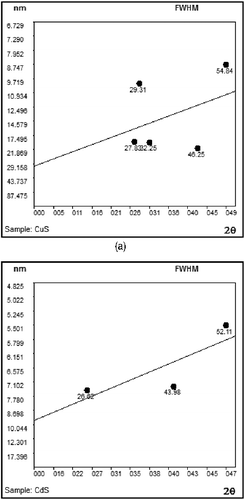
In order to understand the structural properties of the sample, crystallite size and strain calculations are required. The crystallite size and lattice strain are the two factors that contribute to the peak broadening. The peak broadening can be caused from defects like residual stress, grain size, distortion and twinning present in the material [Citation16]. The crystallite size and lattice strain were estimated by XPowder software according to Williamson-Hall (W-H) equation given by the following EquationEquation (4)(4)
(4) [Citation16]
(4)
(4) where β is full-width at half-maxima (FWHM) in radians, θ is the diffraction angle, K is the shape factor (K = 0.9), λ is the wavelength of X-rays, Φ is the crystallite size and ϵ is strain. a and b depicts the Williamson-Hall plot for CTAB capped CuS and CdS nanoparticles with the hexagonal phase respectively. The results of the W-H analysis for the samples give values of Φ and ϵ as 31.12, 0.298, 11.89 and 0.502 nm for the CTAB capped CuS and CdS nanoparticles, respectively. The scattered points corresponding to each crystallographic plane in the W-H plot can be attributed to the anisotropy of the dislocation strain field in the elastic medium, as well as to the contribution of planar defects The average crystallite size obtained from the Williamson-Hall analysis is in agreement with values obtained from Scherrer analysis and HRTEM analysis are listed in .
Figure 4. (a) The Williamson-Hall Plot of CTAB capped CuS nanoparticles. (b) The Williamson-Hall Plot of CTAB capped CdS nanoparticles.
3.2 Morphological characterization
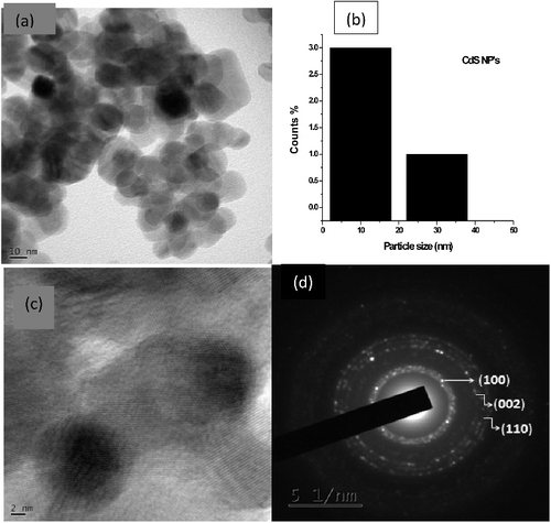
shows the HRTEM micrographs of the hexagonal copper sulfide nanoparticles, which suggest that the hydrothermal synthesis is a potential method, with the advantages of large – scale production and good uniformity of the particles obtained. The statistical information of the mean particle size of nanoparticles was determined to be 34 nm shown in b. In c the measured lattice spacing of 1.960 Å, is consistent with the spacing between [110] planes of CuS nanoparticles. d presents the selected area electron diffraction [SAED] pattern and the ordered hexagonal– like spot arrays confirmed the formation of hexagonal structures of nanoparticles. On the other hand, CTAB played an important role in the formation of hexagonal CuS nanoparticles. shows the HRTEM images of CTAB capped CdS nanoparticles formed as spherical crystallites. By statistical means on the HRTEM image, b reveals the CTAB capped CdS nanoparticles have a mean particle size of 18 nm. The nanoparticles were clearly well identified and no effective aggregations of bulk particles were found, which indicates the effective capping of CTAB on the nanoparticle surfaces. Lattice fringe pattern and size of CdS nanocrystallites areclearly revealed in c. The SAED pattern confirms that the synthesized particles are crystalline in nature.There is another reason to have extra weak diffraction spots in SAED patterns. Some systematically absent diffraction spots appear, which do not change the unit cell, but seem to reduce the symmetry of the structure. Possible multiple scattering effect should be considered. If this is the case, these extra diffraction peaks should not be observed in the corresponding XRD pattern, since no multiple scattering takes place in XRD. When the same SAED pattern is recorded at several areas with different specimen thickness, the relative intensities of these extra spots would be significantly changed. Specimen tilting would also notably change the relative intensities of the extra spots.
Figure 5. (a) HRTEM micrograph of CTAB capped CuS hexagonal nanocrystal, (b) size distribution of the nanoparticles, (c) high resolution electron micrograph and (d) SAED pattern of as prepared nanoparticle.
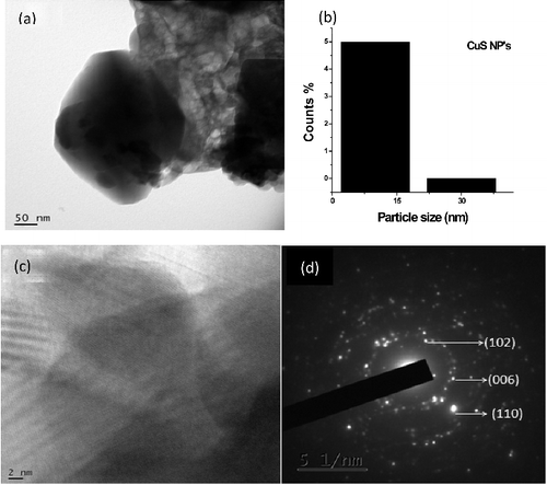
Figure 6. (a) HRTEM micrograph of CdS nanoparticles, (b) particle size distribution of nanoparticles, (c) HRTEM image showing lattice fringes and (d) corresponding SAED pattern.
3.3 FTIR Spectroscopy
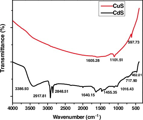
represents the IR spectra of CdS and CuS nanoparticles in the range of 4000–400 cm−1. For CTAB capped CuS nanoparticle, the peak at 1605 cm−1 corresponds to the H-O-H bending of absorbed water, which indicates the existing water molecules are absorbed by sulfur products [Citation17]. The absorption band occurring at 1101 cm−1 is due to asymmetric stretching of carbonyl group (C = O). A vibration peak at 597 cm−1 signifies the presence of Cu-S bond [Citation18,Citation19]. For CTAB capped CdS nanoparticle, the peak at 3386.93 cm−1 is attributed to O-H stretching vibration of water molecules [Citation20]. The CH2 symmetric (νsym(–CH2)) and asymmetric stretching (νasym(–CH2)) vibrations of CTAB bound on CdS nanoparticles are observed at 2917 and 2848 cm−1 respectively [Citation21]. The peaks emerged at 1466.36 cm−1 and 1640.15 cm−1corresponds to the C-C stretching vibrations and the stretching vibrations of sulphate group, traces of SO4−2 ions respectively [Citation18]. The peak at 1016.43 cm−1 is associated to the C = O stretching vibration. The band located at 717.90 cm−1 is correlated to the stretching frequency of Cd-S bond [Citation22].
Figure 7. FTIR Spectra of CTAB capped CdS and CuS Nanoparticles.
3.4 UV diffused reflectance spectral analysis
Optical characterization was examined by the UV-Vis diffuse reflectance spectrum ( and ) and the optical band gap energy is determined by using Kubelka—Munk function F(R) based on the following EquationEquation (5)(5)
(5) [Citation23].
(5)
(5) where R is the function of reflectance and F(R) is proportional to the extinction coefficient (α). The Kubelka—Munk function can be obtained by multiplying the F(R) function by hν using the corresponding coefficient (n) associated with an electronic transition as follows [Citation24]:
(6)
(6)
Figure 8. UV-Vis diffuse reflectance spectra of CTAB capped CdS NPs and the inset, shows the The Kubelka Munk plot for CTAB capped CdS NPs.
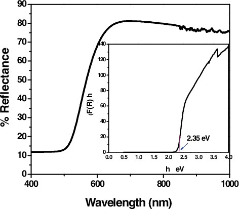
Figure 9. UV-Vis diffuse reflectance spectra of CTAB capped CuS NPs and the inset, shows the The Kubelka Munk plot for CTAB capped CuS NPs.
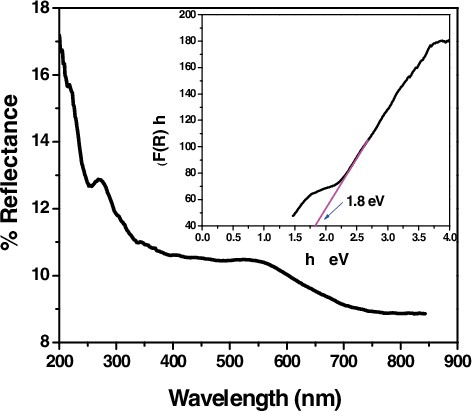
Where, h is the Planck's constant, ν is the frequency of vibration, Eg is the Energy gap, A is the proportionality constant and F(R) is the function of Reflectance and n = 1/2 for a direct allowed band gap transition. In and the inset shows the Kubelka – Munk plot for the calculation of Eg by plotting (F(R)hν)2 versus hν, such a representation is known as the Tauc Method. The value of Ephot extra polated to F(R)E = 0, which gives an absorption energy, corresponds to a band gap Eg. The band gaps of the CTAB capped CdS and CuS samples are approximately equal and are estimated to be 2.35 and 1.8 eV respectively, which is lower than that of the standard bulk CdS and CuS materials. It can be seen that by capping CTAB in CdS and CuS, the band gap energy has decreased, which was similar to the earlier reports [Citation25,Citation26]. The red shifts can be attributed to thecharge transfer transitions between the conduction or valence band of CdS and CuS nanoparticles. Thus it is speculated that this sample may have the highest visible-light driven photocatalytic activity and solar cell application.
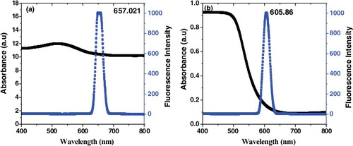
3.5 Photoluminescence spectroscopy
The optical spectra of CdS and CuS nanoparticles are portrayed in a and b. (a) shows the emission spectra of CTAB capped CuS nanoparticles excited at 518 nm. The sharp intense emission peak is located in 657 nm, corresponding to the red emission. The red emission band may be ascribed to the recombination of trapped electron-hole pair, similar behavior was observed by Sharma et al [Citation27] and Deori et al [Citation28]. It is observed that the narrow emission peaks shows better electronic passivation of the CuS nanoparticles by capping CTAB and the reduced broadness of the emission curve may imply a narrow size distribution. The absorption spectrum of (b) shows an excitation peak at 493 nm and the photoluminescence spectrum shows a broad emission peak at 605 nm in red region is observed due to the defects consist of cadmium interstitials or sulfur vacancies in CdS nanoparticles [Citation29,Citation30]. U. Reschet al [Citation31] and Y. Linet al [Citation32] suggested that the sharp emission band is attributed to the radiative recombination of free charge carriers at Cd atom with trapped holes at the sulphur vacancies. The cationic surfactant acting as Lewis acids and depending on their structure, it can stabilize the surface states of the CdS nanoparticles [Citation33]. Several researchers have reported that the adsorbed surfactant acts as, surface passivating agent, which draws more electronic transitions and enhances the PL intensity of the CdS nanoparticles [Citation34–36]. The higher PL intensity of CTAB capped CuS and CdS nanoparticles confirm the high crystallinity and control over size distribution.
Figure 10. Absorption and photoluminescence spectra of (a) CuS and (b) CdS (black axis UV–Vis, blue axis PL).
4. Conclusions
CuS and CdS nanoparticles capped with CTAB have been successfully synthesized using hydrothermal route. XRD pattern showed that the CTAB capped CuS and CdS nanoparticles possess hexagonal phase. The average size of nanocrystallites was about 31 nm for the CuS and 12 nm for CdS. HRTEM images and SAED pattern adequately confirmed the well dispersed and crystalline nature of the metal sulphide nanoparticles. The presence of all the functional groups was observed from FTIR analysis and this study confirmed the presence of Cu-S bond and Cd-S bond. The UV-Vis measurements showed that the band gap of 1.8 eV and 2.3 eV for CuS and CdS nanoparticles, respectively. Emission spectra of the both as-prepared samples were significantly red shifted and the higher PL intensities are attributed to the low defects and high crystallinity. Enhancing the optical properties of the CTAB capped CuS and CdS nanoparticles revealed that these samples can be used in solar cells and optoelectronics.
Acknowledgement
Authors are grateful to UGC minor research project [MRP-5666/15 (SERO/UGC)] for providing financial support to undertake this work.
Disclosure statement
All the authors have declared that no competing financial interests in this article.
References
- Mal J, Nancharaiah YV, Van Hullebusch ED, et al. Metal chalcogenide quantum dots: biotechnological synthesis and applications. RSC Adv. 2016;6:41477–41495.
- Ansari F, Soofivand F, Salavati-Niasari M. Utilizing maleic acid as a novel fuel for synthesis of PbFe12O19 nanoceramics via sol–gel auto-combustion route, Materials Characterization 2015;103:11–17.
- Min Y, Akbulut M, Kristiansen K, et al. The role of interparticle and external forces in nanoparticle assembly. Nat Mater. 2008;7:527–538.
- Dumbrava A, Badea C, Prodan G, et al. Synthesis and characterization of cadmium sulfide obtained at room temperature. Chalcogenide Lett. 2010;7:111–118.
- Mageshwari K, Mali SS, Hemalatha T, et al. Low temperature growth of cus nanoparticles by reflux condensation method. Prog Solid State Ch. 2011;39:108–113.
- Moloto N, Moloto MJ, Kalenga M, et al. Synthesis and characterization of MnS and MnSe nanoparticles: morphology, optical and magnetic properties. Opt Mater. 2014;36:31–35.
- Saldanha PL, Brescia R, Prato M, et al. Generalized one-pot synthesis of copper sulfide, selenide-sulfide, and telluride-sulfide nanoparticles. Chem Mater. 2014;26(3):1442–1449.
- Nemade KR, Waghuley SA. Band gap engineering of CuS nanoparticles for artificial photosynthesis. Mat Sci Semicon Proc. 2015;39:781–785.
- Mehta SK, Kumar S. Photoactivation and perturbation of photoluminescent properties of aqueous ZnS nanoparticles: probing the surfactant-semiconductor interfaces, Mater Chem Phys. 2011;131:94–101.
- Li W, Xiao F, Su H, et al. Investigation of adsorption and photocatalytic activities of in situ cetyltrimethylammonium bromide-modified Bi/BiOClheterojunctionphotocatalyst for organic contaminants removal. RSC Adv. 2016;6:93309–93317.
- Mozaffari S, Li W, Thompson C, et al. Colloidal nanoparticle size control: Experimental and kinetic modeling investigation of the ligand -metal binding role in controlling the nucleation and growth kinetics. Nanoscale. 2017;9:3772–13785.
- Jing C, Gu Z, Ying Y-L, et al. Chrominance to dimension: a real-time method for measuring the size of single gold nanoparticles. Anal Chem.. 2012;84(10):4284–4291.
- Yoshimura M, Byrappa K. Hydrothermal processing of materials: past, present and future. J Mater Sci. 2008;43:2085–2103.
- Han S, Hu L, Gao N, et al. Efficient self-assembly synthesis of uniform CdS spherical nanoparticles-Au nanoparticles hybrids with enhanced photoactivity. Adv Funct Mater. 2014;24:3725–3733.
- Jia B, Mingli Q, Xuezhi J, et al. Synthesis, characterization, shape evolution, and optical properties of copper sulfide hexagonal bifrustumnanocrystals. J Nanopart Res. 2013;15:1469.
- Li Y, Hu Y, Peng S, et al. Synthesis of CdSnanorods by an ethylenediamine assisted hydrothermal method for photocatalytic hydrogen evolution. J Phys Chem. 2009; 113:9352–9358.
- Othman AA, Ali MA, Ibrahim EMM, et al. Influence of Cu doping onstructural, morphological, photoluminescence, and electrical properties of ZnOnanostructures synthesized by ice-bath assisted sonochemical method. J Alloys Compd.. 2016;683:399–411.
- Singh V, Chauhan P. Structural and optical characterization of CdS nanoparticles prepared by chemical precipitation method. J Phys Chem Solids. 2009;70:1074–1079.
- Bahadur J, Agrawal S, Parveen A, et al. Micro-Structural, optical and dielectric properties of Ag doped TiO2 synthesized by sol–gel method, Mater Focus. 2015;4:134–141.
- Pei LZ, Wang JF, Tao XX, et al. Synthesis of CuS and Cu1.1Fe1.1S2 crystals and their electrochemical properties. Mater Charact. 2011;62:354–359.
- Saranya M, Santhosh C, Ramachandran R, et al. Growth of CuS nanostructures by hydrothermal route and its optical properties. J. Nanotechnol. 2014;1–8.
- Nisha KD, Navaneethan M, Hayakawa Y, et al. Structural and morphological evolution of CdSnanosheets-based superstructures by surfactant assisted solvothermal method. Mater Chem Phys. 2012;136:1038–1043
- Sui ZM, Chen X, Wang LY, et al. Capping effect of CTAB on positively charged Ag nanoparticles, Physica E. 2006;33:308–314.
- Kotkata MF, Masoud AE, Mohamed MB, et al. Synthesis and structural characterization of CdS nanoparticles, Physica E. 2009;41:1457–1465.
- Liu J, Lu Y, Liu J, et al. Investigation of near infrared reflectance by tuning the shape of SnO2 nanoparticles. J Alloys Compd. 2010;496:261–264.
- Köferstein R, Jäger L, Ebbinghaus SG. Magnetic and optical investigations on LaFeO3 powders with different particle sizes and corresponding ceramics. Solid State Ionics. 2013;249–250:1–5.
- Bao N, Shen L, Takata T, et al. Facile Cd-Thiourea complex thermolysis synthesis of phase-controlled CdSNanocrystals for photocatalytic hydrogen production under visible light. J Phys Chem. 2007;111:17527–17534.
- Saranya M, Santhosh C, Ramachandran R, et al. Hydrothermal growth of CuS nanostructures and its photocatalytic properties. Powder Technol. 2014;252;25–32.
- Sharma KN, Joshi H, Prakash O, et al. Pyrazole-Stabilized Dinuclear Palladium(II) Chalcogenolates Formed by Oxidative Addition of Bis[2-(4-bromopyrazol-1-yl)ethyl] Dichalcogenides to Palladium(II) – Tailoring of Pd–S/Se Nanoparticles, Eur J Inorg Chem. 2015;4829–4838.
- Deori K, Ujjain SK, Sharma RK, et al. Morphology controlled synthesis of nanoporous Co3O4 nanostructures and their charge storage characteristics in supercapacitors. ACS Appl Mater Interfaces. 2013;5:10665–10672.
- Zhao XS, Schroeder J, Persans PD, et al. Resonant-Raman-scattering and photoluminescence studies in glass-composite and colloidal CdS. Phys Rev B. 1991;43:12580.
- Arul Dhas N, Gedanken A. A sonochemical approach to the surface synthesis of cadmium sulfide nanoparticles on submicron silica. Appl Phys Lett. 1998;72:2514.
- Resch U, Eychmueller A, Haase M, et al. Absorption and fluorescence behavior of redispersible cadmium sulfide colloids in various organic solvents, Langmuir. 1992;8:2215–2218.
- Lin Y, Zhang J, Sargent EH, et al. Photonic pseudo-gap-based modification of photoluminescence from CdSnanocrystal satellites around polymer microspheres in a photonic crystal, Appl. Phys. Lett. 2002;81:3134.
- Diao X-L, Xia Y-S, Zhang T-L, et al. Fluorescence-detecting cationic surfactants using luminescent CdTe quantum dots as probes, Anal Bioanal Chem. 2007;388:1191–1197.
- Kepler KD, Lisensky GC, Patel M, et al. Surface-bound Carbonyl compounds as Lewis acids. Photoluminescence as a probe for the binding of Ketones and Aldehydes to Cadmium Sulfide and Cadmium Selenide Surfaces. J Phys Chem. 1995;99:16011–16017.