
 ?Mathematical formulae have been encoded as MathML and are displayed in this HTML version using MathJax in order to improve their display. Uncheck the box to turn MathJax off. This feature requires Javascript. Click on a formula to zoom.
Abstract
The thrust to invent new materials and technology has been ever increasing due to technological challenges in progressive world. Among new materials, nanomaterials possess superior optical, electrical, magnetic, mechanical, and thermal properties, which have made them suitable for a multitude of applications. The present review paper deals with recent advances in properties of nanostructured glasses and composites in terms optical, electrical, mechanical and thermal properties. A brief discussion has been done on fabrication method of nanostructured glasses. The review of optical properties shows that nanostructured glasses show both direct and indirect band gap and this tuning of band gap depends on extent of nano structuring of samples. The electrical properties also show enhancement in electrical conductivity on nano-structuring of glasses compared to their bulk counterparts. The changes in mechanical and thermal properties of nanostructured glasses and composites are attributed to many microstructural features like grain size and shape, their distribution, pores and their distribution, other flaws/defects and their distribution, surface condition, impurity level, second phases/dopants, stress, duration of its application and temperature effect on the samples. Literature reports that nano structuring leads to enhanced phonon boundary scattering which reduces the thermal conductivity.
1. Introduction
In the rapidly advancing world, it is important to study new materials for new properties and applications. Many new materials have been discovered which show interesting properties for scientific applications [Citation1–11]. Among these materials, nanostructured materials have emerged as boon to mankind. In the past decade, many researchers have invested their time and efforts to study the exciting properties of materials by manipulating their nanostructures. Nanostructured materials having the solid form are most common nanomaterials. Solid nanostructured materials are roughly classified into four categories i.e. powder, fiber, film, and bulk depending on their appearance. They can be Zero-dimensional nanostructures (0D), One-dimensional nanostructures (1D), Two-dimensional nanostructures (2D) and Three-dimensional nanostructures (3D). Zero-dimensional (0D) nanostructures have all three dimensions quantized to nanoscale and are often called quantum dots. In 1D nanostructures, only two dimensions are restricted to nanoscale (e.g. nanowires). In 2D nanostructures, one dimension is quantized to nanoregime (e.g. nanofilms) while 3D nanostructures do not have any quantization at all [Citation12]. These are also known as bulk nanomaterials. Many studies and reviews are focussed on study of these 3D, 2D, 1D and 0D materials [Citation13–19]. The literature [Citation20–25] reports that apart from dimensionality control from 0D to 3D, properties of nanomaterials can also be controlled in terms of their pore size. They are microporous, mesoporous or may have macropores and can be tailored to modify their performance. They are used in rechargeable batteries, gas sensing, supercapacitors, solar cells, electro-/photocatalysis etc. Major developments in nanostructuring of materials are happening in crystalline materials. Many studies have been focussed on the various properties and applications of nano-crystalline materials [Citation26–47]. Some amorphous materials such as glasses and polymers have also contributed substantially to the area of nanotechnology [Citation48–55] and have proved themselves promising in terms of applications. Amorphous alloys are structurally disordered with only short-range order in contrast to crystalline materials, which have long range order with repeating unit cell. Amorphous alloys do not have regular arrangement of atoms, i.e. periodicity, and hence also termed as non-crystalline. These amorphous or non-crystalline materials are sometimes referred as ‘‘glasses’’. While ‘‘non-crystalline’’ is a generic term that describes a solid material having no crystallinity, a ‘glass’ is usually formed by continuous cooling from the liquid. Also, glass is characterized by the presence of a glass transition temperature, Tg. All non-crystalline materials have one feature in common; their structures are such that the sub-unit arrangements can get tangled so easily and so completely in liquid state that they are almost impossible to untangle them once the material is solidified [Citation56–59]. Crystals are well known for their anisotropic nature, where properties in different directions differ considerably. But, amorphous materials particularly glasses have proved interesting due to their varied properties and are widely used as a storage media in optical recording for data storage devices. Glasses are mainly categorized as metallic glasses, chalcogenide glasses and oxide glasses. Metallic glasses are also referred as amorphous metals. These glasses have non-crystalline structure with disordered atomic arrangement. Metallic glasses were first produced by rapidly solidifying metallic melts at cooling rates of about 106K/s [Citation60]. These glasses were produced in different sizes and shapes (ribbons, wires, powders, etc.) by various techniques. Moreover, metallic glasses were found to have excellent mechanical, chemical, and magnetic properties. Some of these techniques have been described in [Citation61–63]. Some of the metallic glasses are Ti–Cu, Ti–Be, Zr–Cu, Zr–Ni, Zr–Ni–Cu etc. Besides metallic glasses, chalcogenide glasses have gained much importance. These glasses contain one or more of any of the chalcogen atoms of group VI, Sulphur, Selenium and Tellurium. Since these glasses contain at least one chalcogen element, they have been have given a name ‘chalcogenide glasses’. Kolomiets [Citation64] suggested that chalcogenide glasses behave as semiconductors and have band gap lying in the range 1 ∼ 3 eV. Ioffe and Regel [Citation65] justified the occurrence of band gap in amorphous glasses by the fact that the band gap in these glasses depends on the existence of short- range order of the lattice. Further, semiconducting behaviour of these glasses is attributed to the presence of covalent bonds existing in these glasses. In chalcogenide glasses, the covalent bonded atoms are arranged with order extending up to the third or fourth nearest neighbours in an open network. Therefore, these glasses are also called network glasses. Examples of chalcogenide glasses are Se-Te, Se-Te-Bi, Se-Te-Sb, Se-Ge-Sb, Se-Ge-Sn etc. Third type of glasses is oxide glasses. These are the oldest glasses and are particularly based on silica. Oxides glasses generally show insulating behaviour and possess large band gap (∼10 eV in case of SiO2). Some of the examples of oxide glasses are Bi2O3–SiO2, Bi2O3–B2O3, Bi2O3–P2O5 , B2O3-Li2O-ZnO-V2O5, Li2Si2O5 etc.
The nanostructurization of glasses is extremely important as it will open new doors of applications with changes in electrical, optical, mechanical, thermal and other properties of these materials. But, fabrication of these glasses at nanoscale is not easy as atomic manipulation is meaningless in a disordered structure, whereas, in crystalline materials, fabrication of atomically flat surfaces can be done with ease by controlling atoms one by one. Moreover, over the crystalline materials, the nanostructured glasses yield a greater variety of properties as the bonding constraint arising from crystalline unit cells does not exist in these glasses. In the past decade, many new developments have been done to study the properties of nanostructured glasses. These glasses have completely different structure than their bulk counterparts. Furthermore, it has also been found that these nanostructured glasses in some cases, show medium-range ordered structure rather than short range order. Therefore, it is evident that by controlling nanostructure formation, properties of these glasses can be tuned as per requirement. In nanostructured glasses, free volume also plays an important role. Free volume of nanoglasses is more than bulk quenched glasses. Free volume affects the structure and properties of these glasses and is also affected by temperatures or stresses. Nanoglasses have enhanced free volume, therefore, glass transition, plastic deformation, structure and properties of nanoglasses are greatly altered. These alterations have evolved entirely new interest in these nanostructured glasses as new properties make these glasses potential candidate for many applications [Citation66–75].
The nanoglasses are found to show two glassy nanostructures such as glassy core and glass-glass interface. Nano-glasses are solid materials composed of nanometer-sized crystalline or nanometer-sized glassy regions connected by crystal/crystal or glass/glass interfaces. As the atomic structures of these interfaces differ from the ones in the building blocks, the atomic and electronic structures of these interfaces differ from the ones in the building blocks. The properties of nanoglasses are different from the conventional glass of the same composition. This has grown interest in researchers to study and modify the properties of glass through nano-structurization. One such technique is plastic deformation, which facilitates the different atomic configurations other than the un-deformed glass at the nanoscale.
The present review article reports the new developments done in various properties of nanostructured glasses and composites. Some of the recent research on optical, electrical, mechanical and thermal properties of these materials have been discussed.
2. Preparation of nanostructured glasses
Many nanostructure materials have been synthesized for various applications in the past years. Several methods are [Citation76–85] available in the literature for preparation of nanomaterials. Among these existing methods, inert-gas consolidation (IGC) method is one of the important methods for synthesis of nanoparticles [Citation77]. This method was introduced by Gleiter and coworkers [Citation78]. In this method, the bulk source material is typically vaporized into a low-density gas under high vacuum of nearly 106 torr, by resistive heating. The vapors of heated sample migrate upwards where the substrate is placed. The substrate is cooled, generally by continuous flow of liquid nitrogen so that by combination of convection and diffusion, sample get deposited on cooled substrate. The cooling of substrate results into rapid decrease in the equilibrium vapor pressure leading to high supersaturation [Citation79]. It is well known that at high supersaturation, the vapors rapidly nucleate, thereby forming very large numbers of extremely small particles lying in nanodimension. The growth of nuclei’s is assisted by Brownian coagulation [Citation80]. The literature reports the synthesis of several types of nanomaterials using this method [Citation51,Citation58, Citation66–70,Citation81,Citation82].
The nanostructured glasses are prepared mostly by inert gas condensation or physical vapor deposition method and thin films of the samples are obtained. shows the schematic diagram of thermal evaporator used for preparation of nanostructured thin films of glassy samples. This arrangement was used by Tripathi et al. [Citation87] and Deepika et al. [Citation88] for fabrication of Se-Te nanostructured thin films. Nanostructures were grown on thin films by pouring liquid nitrogen over the substrate during the film deposition. The arrangement in the vacuum chamber consisted of a molybdenum boat which carries source material and a pre-cleaned glass substrate, which was pasted using a double-sided tape on the circular steel plate located at a vertical distance of 30 cm from source material. The vacuum in the chamber was maintained at 10−5 torr. After attaining the desired vacuum, films were deposited by passing the LT current to the electrodes. During this process, simultaneously, liquid nitrogen was poured over the circular steel plate through a gas inlet. This was done to limit the growth of particles and achieve nanostructure in thin films.
Figure 1. Schematic diagram of thermal evaporator [Citation86] (reprinted with permission from Springer Nature, Copyright 2018).
![Figure 1. Schematic diagram of thermal evaporator [Citation86] (reprinted with permission from Springer Nature, Copyright 2018).](/cms/asset/9ff7b4d5-3819-4b45-921b-c6d6f6de6a58/tjen_a_1940221_f0001_b.jpg)
Besides IGC method, nanoglass films have been recently synthesized by a variety of methods, such as magnetron sputtering [Citation89–92], multiphase pulse electrodeposition [Citation93], and the combination of electron beam and thermal evaporation [Citation94].
3. Properties
3.1. Optical properties
From atoms and molecules to crystals and bulk components, optical materials are naturally structured at different scales. The interaction of materials with optical waves and photons is strongly dependent on the structure, which can then be used to control light field distribution and light propagation. For semiconductor nanoparticles, electron confinement also induces a modulated absorption spectrum. The refractive index is then modified. The bandgap of the material is changed because of the discretization of the electron energy, which can be controlled by the nanometers size particles. The nanostructured glasses especially nano-chalcogenides show a dramatic change in their optical and electronic properties on reduction of size below the excitonic size [Citation95,Citation96]. Depending on the deposition technique used, the micro/nanostructure of thin films can be more or less complex. It is well known that low energy evaporation condensation techniques based on e-beam gun or on heated crucible give columnar thin films for most of the materials [Citation97]. The refractive index of thin films of nanostructured glasses is generally smaller than the refractive index of the bulk material. This is attributed to the lacunar structure of these films [Citation98]. In particular columnar thin films have a packing density that can be much smaller than one. The packing density is given by the ratio of the volume occupied by bulk material over the total volume of the layer [Citation99,Citation100].
3.1.1. Determination of optical properties
The optical study of nanostructured films is carried out using absorption, reflection and transmission spectra recorded on UV-Vis spectrophotometer at room temperature.
3.1.1.1. Calculation of refractive index and film thickness
Swanepoel [Citation101] suggested a theory based on transmittance to obtain the various optical constants of the thin film sample. According to his theory, transmittance (T) is function of α, λ, n, ns and film thickness d and is given by
(1)
(1)
where A = 16n2ns, B=(n + 1)3(n + ns2), C = 2(n2 − 1)(n2 − ns2), D = (n − 1)3(n − ns2), ϕ = 4πnd/λ and x is the absorbance given by x = exp(−αd). EquationEquation (1)
(1)
(1) is proposed for homogeneous thin film of thickness d and complex refractive index nc = n − ik, where n is refractive index and k is extinction coefficient. The substrate is considered to have thickness of several order of magnitude larger than d with refractive index ns. The refractive index of surrounding air is taken as 1. Taking all the multiple reflections at three interfaces into account, in case of k2 ≪ n2, EquationEquation (1)
(1)
(1) can be employed to thin film samples. The values of the transmission at the maxima and minima of the interference fringes can be obtained from EquationEquation (1)
(1)
(1) by setting the interference condition cosϕ = +1 for maxima (TM) and cosϕ = −1 for minima (Tm).
On the basis of Manifacier et al. [Citation102] idea of creating upper and lower envelopes of the interference fringes, Swanepoel proposed the approximate value of refractive index (n1) of the film in the spectral region of medium and weak absorption by the expression
(2)
(2)
where,
(3)
(3)
TM and Tm are the maximum and minimum values of the upper and lower envelopes at a certain wavelength and ns is the refractive index of the glass substrate. The refractive index of the glass substrate (ns) has been calculated from the well known relation [Citation103]
(4)
(4)
where Ts denotes the transmittance spectra of the glass substrate.
If na and nb are the refractive indices at two adjacent maxima (or minima) at wavelengths λ1 and λ2 respectively, then formula for film thickness is given by [Citation104–106],
(5)
(5)
These values are denoted as d1. The d1 values are obtained at different wavelengths and average value is noted as The above equation is derived from the basic equation of interference fringes,
(6)
(6)
where the order number mo is an integer for maxima and a half integer for minima. The
and n1 values are then used to calculate mo for different maxima and minima using EquationEquation (6)
(6)
(6) . The accurate value of film thickness (d2) can now be calculated by taking the exact value of m associated with each maxima or minima. The average value of d2 is denoted as
Now, the value of
and m can be used for each wavelength to obtain improved value of refractive index n2.
3.1.1.2. Determination of optical band gap
The absorption spectra can be used to determine the absorption coefficient (α) using the relation [Citation106]
(7)
(7)
Here, d is the thickness of the film and X is the absorbance. Absorption coefficient can also be employed to determine the nature and value of the energy band gap. The relation between the absorption coefficients (α) and the incident photon energy (hν) is given by [Citation107]:
(8)
(8)
where A is a constant and Eg is the energy band gap of the material and exponent n depends on the type of transition. The values of n for direct allowed, indirect allowed transition and direct forbidden, are given as 1 /2, 2 and 3/ 2 respectively. The energy band gap is calculated from the absorption spectra by plotting a graph between (αhν)1/n and hν. The extrapolation of the straight line to (αhν)1/n = 0 axis gives the value of the energy band gap.
Considerable research has been done on the optical properties of nanostructured glasses in last decade. Khan et al. [Citation70] studied optical properties of a-Se70Te30 nanorods. Their thin films contained nanorods of diameter 30 to 80 nm and length of orders of few hundreds of nanometers. They reported indirect band gap for the samples. Al-Agel [Citation108] studied optical and structural phenomenon in as-deposited thin films composed of aligned nanorods of amorphous SexTe100−x (x = 3, 6, 9, and 12) glasses. On the basis of optical absorption data, they observed a direct optical band gap in their samples. This observation of a direct optical band gap in these nanorods is interesting as chalcogenides normally show an indirect band gap, and due to this reason, these materials could not become very popular for semiconducting devices. shows FESEM images of a-SexTe100−x thin films. It is evident from these images that SexTe100−x thin films contain high yield of short and perfectly aligned nanorods. The diameter of these nanorods was reported between 10 and 20 nm, whereas the length is in the order of several hundred nanometers. shows the plot showing the variation of (α.hν)2 with photon energy (hν) for a-SexTe100−x films composed of aligned nanorods. Their studies reveal that due to this size reduction, the optical properties show a dramatic change and the optical band gap becomes direct. The values of optical constants (refractive index and extinction coefficient) are also enhanced significantly as compared to results from their previous report [Citation109]. This enhancement in the value of optical band gap and optical constants are attributed to the phenomena of size effect. Salah et al. [Citation110] studied the optical properties of thin films of Te94Se6 nanoparticles synthesized using physical vapor condensation technique at different Ar pressures. SEM images () display uniform nanoparticles in these films where the size increases from ∼12 to about 60 nm by decreasing Ar pressure from 667 to 267 Pa. These as-grown thin films were found to have direct band gaps, whose value decreases with increasing particle size. Argon pressure was found to be effective for controlling the particle size. The sizes of the grown nanoparticles were significantly reduced by increasing Ar pressure. These results might be useful for development of optical disks and other semiconducting devices based on these controlled direct band gap. Alvi [Citation111] studied the optical properties of Se77Sb15Ge8 nano-structured thin films. The average particle size lies in the range 30–60 nm. The detailed examination of the data of optical absorption points out that the optical transition is indirect in nature. The optical band gap is viewed around 1.53 eV. In their another study [Citation112], they studied the optical properties of Bi doped Se-Te nanostructured thin films. The band gap of the samples was indirect and was found to increase on nanostructure formation. This was due to decrease in disorderness and defects in the system. Further, they reported that large refractive index and small extinction coefficient of these films makes them suitable for antireflection multi layers.
Figure 2. FESEM images of thin films composed of a-SexTe100−x aligned nanorods [Citation108] (reprinted with permission from Springer Nature, Copyright 2013).
![Figure 2. FESEM images of thin films composed of a-SexTe100−x aligned nanorods [Citation108] (reprinted with permission from Springer Nature, Copyright 2013).](/cms/asset/5f284ac4-0283-4329-a402-215ae6b6ded8/tjen_a_1940221_f0002_b.jpg)
Figure 3. (αhν)2 against photon energy (hν) in a-SexTe100−x thin films composed of aligned nanorods [Citation108] (reprinted with permission from Springer Nature, Copyright 2013).
![Figure 3. (αhν)2 against photon energy (hν) in a-SexTe100−x thin films composed of aligned nanorods [Citation108] (reprinted with permission from Springer Nature, Copyright 2013).](/cms/asset/150ffab3-f5fe-4d1b-ad80-f7d366166ace/tjen_a_1940221_f0003_c.jpg)
Figure 4. SEM image of the as-synthesized thin film of Se6Te94 nanoparticles at Ar pressure 400 pa [Citation110] (reprinted with permission from Elsevier, Copyright 2013).
![Figure 4. SEM image of the as-synthesized thin film of Se6Te94 nanoparticles at Ar pressure 400 pa [Citation110] (reprinted with permission from Elsevier, Copyright 2013).](/cms/asset/a4d70366-2fd6-46b3-a1e3-4833c97833a8/tjen_a_1940221_f0004_b.jpg)
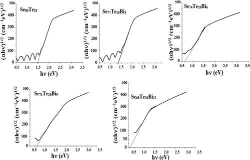
Authors have also carried out considerable work on nanostructured glasses. They have studied the effect of nanorods formation on optical properties of Se-Te-Bi films [Citation113]. For nanostructured Se-Te-Bi system, the band gap values were found to be low as compared to bulk samples [Citation114]. Their results [Citation113] show that energy band gap decreases on increase in Bi concentration in Se-Te-Bi nanostructured system. This was attributed to the presence of large number of unsaturated bonds and structural defects in the system. The higher concentration of defect states increases the number of localized states which eventually narrows the optical band gap. shows transmission spectra of thin films of Se80-xTe20Bix (0 ≤ x ≤ 12) containing nanorods and shows the plot of (αhν)1/2 versus hv for thin films of Se80-xTe20Bix (0 ≤ x ≤ 12) glasses. The band gap was found to be indirect and lower than corresponding bulk sample of nearly same composition. The other studies of authors in this field include optical characterization of nanostructured Ge1-xSnxSe2.5 (x = 0, 0.3, 0.5) films [Citation86], optical properties of nanostructured Se58Ge39Pb3 and Se58Ge36Pb6 thin films [Citation115] and structural and optical study of nanostructured Se80-xTe20Sbx (0 ≤ x ≤ 12) thin films [Citation116].
Figure 5. Transmission spectra of nanostructured thin films of Se80-xTe20Bix (0≤x ≤ 12) glassy alloys [Citation113].
![Figure 5. Transmission spectra of nanostructured thin films of Se80-xTe20Bix (0≤x ≤ 12) glassy alloys [Citation113].](/cms/asset/9b7b31dd-98d0-4c90-985e-0e3e1b4bebc7/tjen_a_1940221_f0005_c.jpg)
Figure 6. Plot of (αhν)1/2 versus hυ for thin films of nanostructured Se80-xTe20Bix (0≤x ≤ 12) glassy alloys.
The most recent studies in optical properties were carried out on the plasmon field enhanced light-induced changes in amorphous Ge24Se76 layer incorporating Au nanoparticles [Citation117]. The presence of gold nanoobjects in amorphous chalcogenide/gold heterostructure influences the optical and structural properties, as well as volume changes of the material. Their results show that superposition of the localized plasmon field of the nanoparticles with the electromagnetic field of incident photons, during the irradiation enhances the light-induced transformations. In another study, a new approach for nano-structuring of glassy Selenium (g-Se) using silver nanoparticles (AgNPs) as precursor has been discussed by Amit Kumar et al. [Citation118]. They synthesized the nano-structured g-Se with the help of silver nanoparticles. It was found that the addition of AgNPs in glassy Se creates fine nano-wires of trigonal Selenium (t-Se) in the glass matrix of g-Se. Further, they have studied electrical, mechanical, and thermal properties of the Ag doped glassy nanocomposite material using current-voltage characteristics, d.c. conductivity, micro-hardness, and kinetic parameters of glass/crystal phase transformation. Their calorimetric results depict that the glass-forming ability and thermal stability of g-Se/AgNPs nanocomposite is greater than Se98Ag2 glass. Further, the nanocomposite sample was found to be harder than the Se98Ag2 alloy which is confirmed by the values of their Vickers hardness number. Furthermore, their results show that d.c. conductivity of g-Se/AgNPs nanocomposite sample is increased appreciably as compared to g-Se98Ag2 sample.
Besides nanostructured chalcogenide glasses discussed above, some studies are also reported on optical properties of nanostructured metallic and oxide glasses. Ning Wang et al. [Citation119] prepared the 3D nanostructure rutile TiO2 photocatalyst by dealloying method using Cu60Ti30Y10 amorphous ribbons as precursors. Their morphological images show that the synthesized rutile TiO2 nano-material presents homogeneous distributed 3D nanoflowers structure, which is composed of large quantities of fine rice-like nanorods (40–150 nm in diameter and 100–250 nm in length). For the sake of convenience, Cu60Ti30Y10, Cu60Ti30Al10, Cu70Ti30 and Cu60Ti30Sn10 amorphous ribbons are labelled as the CTY, CTA, CT and CTS sample, respectively, while Cu60Ti30Y10 amorphous ribbons subjected to immersion in 14.4 M HNO3 aqueous solution at 343 K for 3, 24 and 72 h are denoted as the CTY-3, CTY-24 and CTY-72 sample, respectively. Besides, the sample prepared by dealloying Cu70Ti30 in 14.4 M HNO3 solution at 343 K for 72 h is denoted as the CT-72 sample. shows the SEM images of the samples: (a) CTY-3; (b) CTY-24; (c) CTY-72; (d) CT-72. The photocatalytic activities of the samples were evaluated by degrading rhodamine B (RhB) dye (10 mg/L) under the irradiation of both simulated visible light (>420 nm) and ultraviolet (UV) light (=365 nm). The results of their study show that the photocatalytic activity of rutile TiO2 prepared by dealloying Cu60Ti30Y10 amorphous ribbons is higher than those of commercial rutile and the sample synthesized by dealloying Cu70Ti30 precursors. Min Zhou et al. [Citation120] fabricated nanoporous structures through chemical dealloying from quaternary Zr65Cu17.5Fe10Al7.5 amorphous ribbons. A three-dimensional bi-continuous nanoporous copper (NPC) structure was formed on Zr65Cu17.5Fe10Al7.5 ribbon alloys having the pore sizes of 44.91 nm, 52.60 nm and 57.37 nm, respectively, after immersion in 0.02 M HF solution for 15 h, 20 h, and 25 h. The results show that the pore size of NPC structure increases with increasing the dealloying time. displays the nanoporous structure of Zr65Cu17.5Fe10Al7.5 amorphous ribbons after dealloying in 0.02 M, 0.035 M and 0.05 M HF solutions for 5 h. Abhiram Jagannathan et al. [Citation121] studied nonlinear optical properties of gold nanoparticles doped fluoroborate glasses for optical limiting applications. High resolution-transmission electron microscopic (HR-TEM) measurements further confirmed the existence of spherical and ellipsoidal Au NPs (). They reported that optical bandgap values were red shifted for samples doped with gold nanoparticles and having more concentration of lithium content. These sample show better nonlinear refractive index and nonlinear absorption coefficient. Weldegrum et al. [Citation122] studied hybrid ZnO nanowires (ZnO-NWs)/metallic nanotube arrays (MeNTA) structure. MeNTA was formed using sputter-deposition of five different metallic glasses. Optical properties were studied and results confirm the formation of nanowires having the hexagonal wurtzite structure. Also, they show strong UV emissions, which can be used in optoelectronics, sensors, piezoelectric-nanogenerator, solar cells and battery applications.
Figure 7. SEM images of the samples: (a) CTY-3; (b) CTY-24; (c) CTY-72; (d) CT-72 [Citation119] (reprinted with permission from Elsevier, Copyright 2018).
![Figure 7. SEM images of the samples: (a) CTY-3; (b) CTY-24; (c) CTY-72; (d) CT-72 [Citation119] (reprinted with permission from Elsevier, Copyright 2018).](/cms/asset/b285e547-1da1-459d-9db0-baf1102e8601/tjen_a_1940221_f0007_b.jpg)
Figure 8. FESEM morphologies of Zr65Cu17.5Fe10Al7.5 amorphous ribbons after dealloying in (a) 0.02 M, (b) 0.035 M, (c) 0.05 M HF solutions for 5 h [Citation120] (reprinted with permission from Elsevier, Copyright 2017).
![Figure 8. FESEM morphologies of Zr65Cu17.5Fe10Al7.5 amorphous ribbons after dealloying in (a) 0.02 M, (b) 0.035 M, (c) 0.05 M HF solutions for 5 h [Citation120] (reprinted with permission from Elsevier, Copyright 2017).](/cms/asset/bd748901-9dff-4cd9-b21f-0780ac4cbd94/tjen_a_1940221_f0008_b.jpg)
Figure 9. HRTEM image confirming uniform distribution of Au NP's in Glass (a)HRTEM image of 2 nm Au NP's depicts the inter planar distance of Au [Citation121] (reprinted with permission from Elsevier, Copyright 2020).
![Figure 9. HRTEM image confirming uniform distribution of Au NP's in Glass (a)HRTEM image of 2 nm Au NP's depicts the inter planar distance of Au [Citation121] (reprinted with permission from Elsevier, Copyright 2020).](/cms/asset/25bb295d-ca22-4b36-a6f9-419fee2bceb4/tjen_a_1940221_f0009_b.jpg)
3.2. Electrical properties
Electrical properties of the materials are important for selection of material for a device. The electrical properties of the nanostructured glasses and composites have led to several applications in electronic and opto-electronic devices. In contrast to crystalline solids, the theory of electronic band structure and the mechanism of electron transport in semiconducting glasses are not well understood. It is generally agreed, however, that the band structure in glasses is not drastically different from that of analogous ordered structures and that the forbidden gap may persist [Citation123]. The major change on transitions from a crystalline to disordered structure is the introduction of ‘tails’ of localized state in the forbidden gap [Citation124] Two types of conduction processes are possible in amorphous solids. An electron in a localized state can make a transition directly to a neighbouring localized state. At each transition energy is exchanged with the lattice through interaction with phonons; (hopping conduction). On the other hand, an electron (or hole) can be excited to the conduction band (or valence band) where it can drift in the same way as in crystalline semiconductors and be subjected to the same type of scattering and trapping mechanisms. In addition, the drift mobility will be affected by the disappearance of periodicity and because of the high density of localized state the mobility may become severely trap limited. The section below discusses the basic methods to study the electrical properties of nanostructured glasses.
3.2.1. Determination of electrical properties
Electrical properties of nanostructured glasses largely depend on defects, grain size, density distributions and doped impurities. It is reported that nanostructures of glasses comprise of nanometer –sized glassy clusters connected by glass-glass interface of reduced density, reduced nearest –neighbour atoms and different electronic structure. These changes in atomic and electronic structures lead to entirely different electrical properties of the system compared to bulk glasses of the same composition [Citation125]. These interesting properties have led their applications in nanoelectronic devices, optical memory devices, fabrication of nanomemories etc. [Citation126–128].
3.2.1.1. Calculation of dc electrical conductivity
To determine the dc electrical conductivity, the I-V curves of the nanostructured samples are recorded on Keithley electrometer and are linearly fitted. The slope of the curves is used to evaluate the dc electrical conductivity using the following relation [Citation129,Citation130]:
(9)
(9)
where, R denotes resistance, L and A are thickness and cross-sectional area of the sample respectively. A graph is plotted between 1000/T versus ln σdc for the samples. The plots are fitted to straight line and slope of the straight line gives activation energy of conduction (ΔE) while the intercept gives pre-exponential factor (σo). The dc electrical conductivity is dependent on temperature through the Arrhenius equation given by [Citation131,Citation132]
(10)
(10)
where, ΔE is activation energy of conduction, σo represents the pre-exponential factor and K is Boltzmann constant.
In the low temperature region (303–343 K), dependence of electrical conductivity on temperature could be studied using Mott’s three-dimensional variable range hopping model (3D VRH) given by [Citation130]
The slope of the plot gives the value of B and intercept is pre-exponential factor. The value of B [Citation130] is equivalent to
(11)
(11)
Here, α−1 denotes spatial extent of the wave function exp(-αR) associated with the localized states, λ is a dimensionless constant (about 18), N(Ef) is the density of localized states near the fermi level, To is degree of disorder and k is Boltzmann constant.
The value of pre-exponential factor is given by [Citation131,Citation132]
(12)
(12)
where γ is Debye frequency (about 1013 Hz) [Citation133] and e is the electronic charge.
3.2.1.2. Solving simultaneously EquationEquations (3) (3) (3) and Equation(4)(4) (4) gives
The values of N(Ef) indicate that number of states available near the fermi level for conduction. The values of α and N (Ef) can be used to determine hopping range (R) and hopping energy (W) using the following relations [Citation131,Citation132]
(15)
(15)
(16)
(16)
The values of R and W are also helpful in ascertaining the conduction mechanism taking place in glassy systems.
Some of the studies carried out on electrical properties of nanostructured glasses are discussed. Alvi [Citation111] studied the electrical properties of Se77Sb15Ge8 nano-structured thin films. The dc activation energy (σdc) in nano-structured Se77Sb15Ge8 thin films was calculated from the temperature dependence and was found to be 1.23 eV. Moreover, σdc increases exponentially with temperature, which demonstrates that the conduction in these glassy alloys takes in the course of an activated procedure and also indicates the semiconducting nature of these alloys. displays the temperature dependence of σdc of nano-structured Se77Sb15Ge8 thin film. Figure clearly indicates that with increasing temperature, σdc increases exponentially with temperature. Mohd. Nasir and M. Zulfequar [Citation134] have studied space charge limited conduction (SCLC) on the fabricated thin films of Se95−xSxZn5 (0.2 ≤ x ≤ 10) in temperature range 313–353 K. They calculated the dc conductivity and activation energy and it was found to decrease and increase respectively, with the increase of sulfur concentration. They observed an ohmic and non-ohmic behaviour both in the low field (≤103 V/cm) and a non-ohmic behaviour is observed due to predominant charge injection from the electrode gap to the samples at high field (∼104 V/cm). Further, they reported that dc conductivity decreases due to increase of nanocrystalline phase in Se95−xSxZn5 alloys. Khan et al. [Citation66] studied the effect of composition on electrical properties of thin films of amorphous GaxSe100-x nanorods. TEM image of these nanorods is presented in . It is clear from the image that the diameter of the nanorods varies from 140 to 180 nm, and the length is of several hundreds of nanometers. DC electrical conductivity of deposited thin films of a-GaxSe100-x nanorods is measured as a function of temperature range from 298 to 383 K. An exponential increase in the dc conductivity is observed with the increase in temperature, suggesting thereby a semiconducting behavior. shows the temperature dependence of dc conductivity in the temperature range (298–383 K) at various concentration of Ga of thin films of a-GaxSe100-x nanorods. The estimated value of activation energy decreases on incorporation of dopant (Ga) content in the Se system. The calculated value of pre-exponential factor (σo) is of the order of 10−1 cm−1, which suggests that the conduction takes place in the band tails of localized states. It is suggested that the conduction is due to thermally assisted tunnelling of the carriers in the localized states near the band edges. In another communication, Khan et al. [Citation135] studied electrical transport properties of films of Se87Te13 nanorods. The dc conductivity for these nanorods as studied as a function of over a temperature range of 500–100 K. Both thermally activated process and variable range hopping mechanism were reported responsible for electrical transport process.
Figure 10. Variation of ln(σdc ) versus 1000/T graph of nano-structured Se77Sb15Ge8 thin films [Citation111] (reprinted with permission from Elsevier, Copyright 2016).
![Figure 10. Variation of ln(σdc ) versus 1000/T graph of nano-structured Se77Sb15Ge8 thin films [Citation111] (reprinted with permission from Elsevier, Copyright 2016).](/cms/asset/2bd06610-4300-4c7a-8b84-fc3b1d38cfe9/tjen_a_1940221_f0010_c.jpg)
Figure 11. TEM image of a-Ga12Se88 nanorods [Citation66] (reprinted with permission from Springer Nature, Copyright 2010).
![Figure 11. TEM image of a-Ga12Se88 nanorods [Citation66] (reprinted with permission from Springer Nature, Copyright 2010).](/cms/asset/8cb4a9fb-3b77-4d4b-8fb8-2b76c77bb713/tjen_a_1940221_f0011_c.jpg)
Figure 12. Temperature dependence of dc conductivity in the temperature range (298–383 K) at various concentration of Ga of thin films of a-GaxSe100-x nanorods [Citation66] (reprinted with permission from Springer Nature, Copyright 2010).
![Figure 12. Temperature dependence of dc conductivity in the temperature range (298–383 K) at various concentration of Ga of thin films of a-GaxSe100-x nanorods [Citation66] (reprinted with permission from Springer Nature, Copyright 2010).](/cms/asset/38c447f4-ea99-43f1-a5c7-b525e68bdf7c/tjen_a_1940221_f0012_c.jpg)
The authors have studied the electrical conduction mechanism in several nanostructured glasses. Electrical properties of films of Se80-xTe20Bix (0 ≤ x ≤ 12) glassy alloys [Citation131] has been studied. The TEM results () indicate the formation of nanorods within the films. The electrical conductivity of the samples was studied using Keithley electrometer in the temperature range 303–373 K. shows the variation of dc electrical conductivity with temperature for Se80-xTe20Bix (0 ≤ x ≤ 12) films. The results show that conduction in these samples takes place via thermally assisted tunnelling and variable range hopping of charge carriers corresponding to higher and lower temperature ranges respectively. shows the plot of ln σ√T with T−1/4 for Se80-xTe20Bix (0 ≤ x ≤ 12) films in the temperature range 303–343 K.
Figure 13. TEM images of nanostructured thin films of Se80-xTe20Bix (0≤x ≤ 12) glassy alloys. (a) Se80Te20 (b) Se77Te20Bi3 (c) Se74Te20Bi6 (d) Se71Te20Bi9 (e) Se68Te20Bi12 [Citation132] (reprinted with permission from Canadian Science Publishing, Copyright 2019).
![Figure 13. TEM images of nanostructured thin films of Se80-xTe20Bix (0≤x ≤ 12) glassy alloys. (a) Se80Te20 (b) Se77Te20Bi3 (c) Se74Te20Bi6 (d) Se71Te20Bi9 (e) Se68Te20Bi12 [Citation132] (reprinted with permission from Canadian Science Publishing, Copyright 2019).](/cms/asset/4c75d78b-947a-4c09-a83a-47208f7fdcd7/tjen_a_1940221_f0013_c.jpg)
Figure 14. Variation of dc electrical conductivity with temperature for Se80-xTe20Bix (0≤x ≤ 12) films [Citation131] (reprinted with permission from Canadian Science Publishing, Copyright 2019).
![Figure 14. Variation of dc electrical conductivity with temperature for Se80-xTe20Bix (0≤x ≤ 12) films [Citation131] (reprinted with permission from Canadian Science Publishing, Copyright 2019).](/cms/asset/5b85304d-c7ac-4a6d-b992-10ac0912bde8/tjen_a_1940221_f0014_c.jpg)
Figure 15. Plot of ln σ√T with T−1/4 for Se80-xTe20Bix (0≤x ≤ 12) films in the temperature range 303–343 K [Citation131] (reprinted with permission from Canadian Science Publishing, Copyright 2019).
![Figure 15. Plot of ln σ√T with T−1/4 for Se80-xTe20Bix (0≤x ≤ 12) films in the temperature range 303–343 K [Citation131] (reprinted with permission from Canadian Science Publishing, Copyright 2019).](/cms/asset/2d6c7a7a-5e93-446b-a6d8-de5c38284b30/tjen_a_1940221_f0015_b.jpg)
It can be noticed that conductivity increases sluggishly with temperature, which suggest that conduction takes place via variable range hopping (VRH). Authors have also studied the electrical properties of Se80-xTe20Sbx (0 ≤ x ≤ 12) nanorods as a function of temperature and composition [Citation132]. Two conduction mechanisms were observed in the Se80-xTe20Sbx (0 ≤ x ≤ 12) system. In higher temperature range (343–373 K), conduction takes place through thermally assisted tunnelling of charge carriers while in the temperature range 303–343 K, variable range hopping of charge carriers contributes to conduction. Moreover, it was found that nanostructure formation augments the electrical conductivity by order of 104 as compared to its bulk counterparts.
3.3. Mechanical properties
Mechanical properties of a material are largely dependent on the structural arrangement of atoms and nature of bonds between them. The addition of impurities and presence of defects affect the mechanical properties of a material. Some of the mechanical properties of solids are elasticity and plasticity, stress, strain and elastic moduli. Mechanical properties of solids elaborate the characteristics such as the resistance to deformation and their strength. These properties play an important role in determining potency of solids in various applications [Citation136–142].
The development of nanostructured materials is now raising the question on change of different properties as the microstructural scale is reduced to nanometer dimensions. Among potential applications of nanostructured materials, the design to achieve optimum mechanical properties is a common concern. The mechanical strength (σ) of crystalline materials is believed to be largely controlled by the grain size (d), and is generally described by the Hall-Petch relationship [Citation143]
(17)
(17)
As the structural scale reduces to the nanometer range, new mechanisms may come into play due to small dimensions. In addition, the intrinsically high interface to-volume ratio of the nanostructured materials may enhance interface-driven processes to extend the strain to failure and plasticity. The mechanical properties of nanoparticles allow their novel applications in many fields, e.g. surface engineering, tribology and nanomanufacturing/nanofabrication. Understanding some basic mechanical properties of nanoparticles, such as the hardness and the elastic modulus, will aid a lot in the proper design of particles in specific applications, as well as evaluating their roles and action mechanisms [Citation144–146]. It has been pointed out that [Citation147–149] many microstructural features like grain size and shape, their distribution, pores and their distribution, other flaws/defects and their distribution, surface condition, impurity level, second phases/dopants, stress, duration of its application and temperature affect the mechanical properties of nanocrystalline (n-) materials. For crystalline metal nanoparticles, dislocations inside the particles have been demonstrated as one of the factors contributing to the change in the mechanical behaviour of nanoparticles, which is in contrast to the traditional view that no dislocation is present in crystalline nanoparticles. Apart from dislocations or defects, the changes of the lattice strain and the bond energies of nanoparticles to the compressive stress are another cause for the strengthening and weakening of the mechanical properties of nanoparticles [Citation147–149]. Very few studies have been carried out on mechanical properties of nanostructured glasses. Vella et al. [Citation150] studied the mechanical properties of nanostructured amorphous CuNb, FeB, and FeTi metal multilayer thin films. The hardness of amorphous metal multilayered films was investigated by nanoindenation. Bilayer material systems of amorphous CuNb, FeB, and FeTi were produced by dc sputtering on sapphire substrates to a total thickness of 1 μm. The bilayer periods (Λ) ranged from 2 to 50 nm. The hardness behaviour is in contrast with the behaviour of crystalline multilayered films, which generally display significant enhancements as the bilayer period is decreased below 10 nm. The lack of a significant hardness variation in the amorphous films strongly suggests that dislocation-mediated mechanisms do not govern inhomogeneous flow in amorphous metals. Xuning Xue et al. [Citation151] studied the microhardness of chalcogenide glasses (ChGs) and glass–ceramics of the Sn-Sb-Se Ternary System. The mechanical property of ChGs was investigated in terms of microhardness (HV), and the relationship between HV and mean coordination number (MCN) (related to the chemical order of the ChG network) was studied. The microhardness of ChGs of the Sn-Sb-Se (SSS) ternary system was investigated. Microhardness rapidly increased as the MCN of the SSS ChGs approached 2.4, signifying the transition of the SSS glass network from under-cross-linked floppy to over-constrained rigid state. Kancherla et al. [Citation152] studied the mechanical properties of glass fabric composite with surfactant treated zirconia nanoparticles. The optimal dispersion of yttria stabilized zirconia (YSZ) nanoparticles in matrix-fabric system was carried out. The study reports that the dispersion of as low as 3 wt% of YSZ is found to be optimal for the developed processing condition. The enhancement is due to two-fold effects, one is the nano-cluster segregation by surfactant and the other one is an optimal interfacial stress/fracture modification in the matrix-fabric system via optimal length-scale effects of nano-composite with respect to the fabric interface. Saida et al. [Citation153] studied the nanostructured materials based on Zr-Al-Ni-Cu metallic glasses. They found that the nanoscale structure control in metallic glasses exhibits unique mechanical properties such as a high strength and good ductility. They investigated the transformation from the glassy state to the nanoscale primary phase in the Zr65Al7.5Ni10Cu17.5-xPdx (x = 0, 5, 10 and 17.5) metallic glasses. The nucleation and grain growth kinetics were examined and it was found that it was easy to control the nanostructure in the Zr-based BMGs by the Pd addition and it was also possible to improve the mechanical properties by the nanoparticle precipitation. Chen et al. [Citation89] studied formation and properties of Au-based nanograined metallic glasses. Gold-based nanograined metallic glass (NGMG) exhibits a heterogeneous granular structure but possess a glassy nature. The smallest particle size of the NGMG can be less than 10 nm. NGMG sustains the good mechanical properties of metallic glasses, showing a high hardness of ∼5.3 GPa. In addition to the nanostructure-induced catalytic functionality, this material sustains the good mechanical properties of a metallic glassy structure, showing a high hardness and a low elastic modulus. Yvonne Ritter et al. [Citation154] studied structure, stability and mechanical properties of internal interfaces in Cu64Zr36 nanoglasses by MD simulations. Their results provide evidence for the existence of glass–glass interfaces, which are characterized by a defective short-range order and an excess free volume of about 1–2%. Jian et al. [Citation155] studied the strength, hardness and ductility of Cu64Zr36 nanoglasses via embedded nanocrystals. They reported that with an increasing fraction of nanocrystalline grains, the tensile strength of the composite is enhanced, while its ductility decreases. Further, they inferred that for an appropriate fraction of nanocrystalline grains, a good balance among strength, hardness and ductility can be realized, which is useful for the synthesis of novel nanograined glass/crystalline composites with high strength, high hardness and superior ductility.
3.4. Thermal properties
Thermal properties play an important role in determining the application of material [Citation156–159]. Thermal properties include knowledge of flow of heat from one place to another. Several methods have been studied for heat flow in materials [Citation160–163]. For heat flow in crystalline nanomaterials, energy carriers are mainly crystal vibrations or phonons. These phonons travel through lattice vibrations and have characteristic lengths of the order of nanometers. The thermal properties of material are characterized by thermal conductivity (k), specific heat (cp) and thermal diffusivity(α). These properties are greatly affected by intrinsic electron–phonon and phonon–phonon scatterings, grain boundaries, surface interactions, grain size and temperature [Citation164]. In nanostructured glasses, motion of phonons is hindered due to disordered structure. The primary means of thermal transport in these glasses are disordered diffusion between high-energy localized vibrational modes (LVMs). The thermal conductivity (k) of nanostructured glasses mainly depends on disorderness and temperature of material [Citation165]. In crystalline nanomaterials, both electrons and phonons play vital role in transfer of heat energy while in amorphous nanostructured glasses, phonons are primary energy carriers responsible for thermal transport [Citation165]. Moreover, in nanostructured materials, the mean free path (MFP) of phonons and the wave vectors has dimensions of nanoscale [Citation166]. Therefore, MFP distribution of phonons in nanostructured glasses play an important key to understand the thermal transport characteristics of phonons as carriers of thermal energy. But, thermal conductivity is significantly reduced compared to bulk material, due to scattering of nanomaterials at the interface.
For amorphous nanomaterials like nanostructured glasses, the dominant factor affecting thermal conductivity is the degrees of disorder (ε). Degrees of disorder (ε) is a strong indicator of the thermal transport properties of materials. A very low value of ε indicates a ordered structure and has extremely high value of thermal conductivity (k) up to 5300 W/m K [Citation165] whereas, a high ε correspond to disordered structure. For such a material, the k is close to that of an insulator typically below 1 W/m K [Citation165]. However, if the ε is quite high then, the phonon velocity and polarization direction inside the structure is not useful to evaluate the thermophysical properties. Moreover, it is found that the heat conduction mainly depends on both phonons and diffusions for value of ε lying between 0–1. Therefore, for amorphous nanostructures such as nanoglasses having higher degree of disorder, the thermal conductivity (k) is said to consists of two parts [Citation166]:
(18)
(18)
where kP denotes the contribution by phonons from propagating modes, and kD represents the contribution by diffusions from nonpropagating modes given by the Allen–Feldman (AF) theory [Citation167,Citation168]. The contributions due to phonons (kP) has been obtained using the specific heat (cp) in different modes and vibrational density of states (VDOS) of phonons [Citation166]. For calculation of kp, it was assumed that the system is isotropic and has a single polarization, so that mode properties are only related to ω [Citation167,Citation168]:
(19)
(19)
where Vs is the volume of system, ωcut denotes the cutoff frequency of phonon, D(ω) is vibrational density of states, C(ω) is mode specific heat capacity and α (ω) =
τ (ω)/3 is mode thermal diffusivity of the vibration mode related to ω. Phonon lifetime is represented by τ (ω) and ss is the sound speed. The phonons contribute to transport when the system frequency is less than ωcut, while diffusions contribute at higher frequencies. For phonons, the density of states (DOS) of the material can be evaluated using the Debye model [Citation166]:
(20)
(20)
The quantum expression for the C(ω) is given by [Citation166]:
(21)
(21)
where kB denotes the Boltzmann constant. Similarly, the contribution of diffusions to k can be obtained from the C in different modes and α [Citation167,Citation168]:
(22)
(22)
where vibration frequency of the ith localized mode is ωi , C(ωi) denotes the diffusion isobaric specific heat capacity, and α(ωi) is the diffusion diffusivity of the ith localized mode. The AF theory [Citation167] can be employed to determine the thermal diffusivity (α) of the localized mode using the relation
(23)
(23)
where Mij is the thermal coupling between ith modes and jth modes, which can be calculated by the modal frequencies and the spatial overlap of mode vectors.
The determination of thermal conductivity (k) depends on many factors. Some of the factors are discussed below.
Effect of grain size: The effect of grain size (L) is not negligible in nanostructured glasses. Grain size determines the grain boundary scattering rate, increasing grain size helps in reducing the scattering [Citation168]. Less scattering results in high thermal conductivity.
Effect of grain boundary: By definition, the grain boundary is the interface between the grains with the same structure and orientation. Generally, nanocrystalline (NC) materials are comprised of grains having size in nanoregime (1–10 nm). These grains cover more than 50% of NC materials and the average grain size of grain boundaries is found to be inversely proportional to fractional grain size [Citation169]. The small grain size and large specific surface area brings significant change in thermo-physical properties of NC materials as compared to bulk crystals. The effect of phonon grain boundary scattering on thermal properties of nanostructured materials has been studied widely to study thermoelectric applications of these materials. The grain boundaries present in NC materials can effectively scatter short-wave phonons, thereby reducing the lattice thermal conductivity of the material in the low temperature region. It has also been reported [Citation170] that thermal conductivity due to grain boundary scattering is an index of the cohesive energy of the grain boundaries.
Effect of temperature: Temperature plays an important role in determining thermal conductivity of nanostructure materials as temperature has direct effect on thermophysical properties especially at high temperatures. The study on effect of temperature reveals that thermal conductivity changes with change in temperature and potential application of nanostructure materials can be adjusted by controlling temperature of system.
Effect of defects: Defects are unavoidable in a material. Defects can be in any form like vacancies, impurity atoms, or rough edges. The phonon zero acoustic mode plays a leading role in thermal transport at low temperatures. Further, the stronger the zero acoustic mode scattering, the smaller is the effect of defects on thermal conductivity (k). This is consequence of additional phonon scattering caused due to the localization of phonons near the defect. Therefore, controlling defects and their density together with temperature affect the thermal conductivity of nanostructured materials [Citation171,Citation172].
Beside thermal conductivity, thermal diffusivity (α) is another important parameter to study thermal property of a material. Thermal diffusivity (α) refers to rate of heat transfer in a material. Thermal diffusivity is independent of the amount of energy during heat conduction. It is the rate of diffusion from the hot end to the cold end in the material, and has a transient value. Thermal conductivity (k) and thermal diffusivity (α) are interconnected and the k of the material can be determined by measuring the α and vice versa. The relation between k, density (ρ) and specific heat (cp) is given by [Citation163]:
(24)
(24)
From above relation, it is evident that the higher value of α indicate stronger ability of the medium to balance its internal temperature. Therefore, α is an indicator of the ability of the medium to propagate energy through the material. In other words, α describes the rate of heat transfer from heat source to heat sink. The specific heat capacity (cp) mentioned in EquationEquation (23)(23)
(23) consist of phonon specific heat capacity and electron specific heat capacity. In some nanomaterials, cp is primarily dominated by phonons whereas, in some other materials, electron specific heat capacity plays a major role. The relationship between time (t) and temperature (T) with thermal diffusivity (α) is given by [Citation163]:
(25)
(25)
Substantial work has been done on the thermal properties of nanocrystalline materials. However, work on nanostructured glasses is scanty and done in recent years. Dong et al. [Citation173] proposed a theoretical model for describing effective thermal conductivity (ETC) of nanocrystalline materials on the basis of grain size, single crystal thermal conductivity, single crystal phonon mean free path (PMFP), and the Kaptiza thermal resistance. It has been demonstrated that with increasing grain size, both grain boundaries (GBs) and size effects become weaker, while size effects have stronger effect on thermal conductivity than GBs effects. Wang et al. [Citation174] studied the thermal Conductivity of nanocrystalline silicon. The effect of grain size and temperature on thermal conductivity has been studied. shows k as a function of Davg. for the fully dense samples (ρ > 99%) at three temperatures. At low T, the power law is k ∝ D1, as expected for a system dominated by boundary scattering, while for higher T and larger grains the k(D) power law becomes weaker due to the increasing importance of impurity /defect scattering also called umklapp scattering. Soyez et al. [Citation175] also corroborated that increasing the nanoparticle size is another effective way to boost k. They studied grain-size-dependent thermal conductivity of nanocrystalline yttria-stabilized zirconia (YSZ) films grown by metal-organic chemical vapor deposition. They stated that reduced thermal conductivity in nanocrystalline coatings arises due to enhanced phonon scattering and presence of numerous closely spaced grain boundaries. shows the thermal conductivity for both a 13 nm grain-sized YSZ film and an alumina substrate as a function of temperature. The results indicate that over the narrow measured temperature range, the YSZ thermal conductivity is temperature independent, while the Al2O3 thermal conductivity decreases significantly with increasing temperature. Further, they reported that significant reduction in thermal conductivity in these films compared to that of bulk YSZ is observed for grain sizes smaller than the phonon mean-free path. The authors also reported presence of porosity in the samples, however, the amount of porosity was not observed to vary significantly with grain size. Their results conclude that the observed changes in thermal conductivity are more likely attributable to the effects of grain size than to porosity. Mishra and Kumar [Citation176] have studied the thermal transport properties of Se95-xSn5Bix (x = 0, 4, 8) chalcogenide alloys. Transmission electron microscopy (TEM) demonstrates the formation of nano-rods and clusters of nano-particles. It was observed that thermal conductivity (λe) shows a decreasing trend with the inclusion of Bi in Se–Sn system. Thermal diffusivity (χe) and volumetric heat capacity (QCp) show the optimum value for x = 4. Thermal transport parameters remain almost temperature independent. They stated that nano structuring leads to enhanced phonon boundary scattering which reduces the thermal conductivity. Also, the combined effect of increased boundary phonon scattering and scattering from defects, contributes to the further reduction of thermal conductivity. shows the variation of effective thermal conductivity with temperature for different composition of Bi. The authors have also calculated the phonon mean free path (τ) using the relation:
(26)
(26)
where χ is thermal diffusivity and vs is velocity of sound (mean speed of carriers in a material), in case of chalcogenide glasses which is ≈ − 2000 m/s [Citation177]. Anupama Viswanathan et al. [Citation178] studied the concentration dependent thermal diffusivity of Ge25Se65Sb10 and Ge25Se60Sb10Ag5 chalcogenide glass nanocolloids. Nanocolloids of five different concentrations from each composition were prepared by dissolving finely powdered bulk glasses in organic solvent ethylenediamine (EDA). Enhancement in thermal diffusivity was observed with increase in solute concentration and was attributed to increased number of localised defects states, phonon scattering at particle liquid interface and Brownian motion of the particles. Maryam Mohri et al. [Citation92] investigated the effect of deposition conditions on the microstructure and thermal stability of Ti-Zr-Cu-Pd nano-glass thin films. Nano-grained metallic glass Ti-Zr-Cu-Pd thin films were deposited at room temperature on Si substrate by using direct current (DC) magnetron sputtering with an alloy target. Nanometer-sized glassy clusters were observed in the thin films deposited at higher Ar pressure. Average grain size was noted to decrease while the roughness of the thin films was increased. All of these observations seem to indicate that the sputtering pressure is the dominating factor controlling the microstructure and thermal stability of the sputtered films.
Figure 16. Thermal conductivity vs average grain size for fully dense samples 550 (99%), 144 (99%), and 76 (99%) at three temperatures [Citation174] (reprinted with permission from American Chemical Society, Copyright 2011).
![Figure 16. Thermal conductivity vs average grain size for fully dense samples 550 (99%), 144 (99%), and 76 (99%) at three temperatures [Citation174] (reprinted with permission from American Chemical Society, Copyright 2011).](/cms/asset/8e22c1d4-798a-4993-9e97-bdfccb3cb65c/tjen_a_1940221_f0016_c.jpg)
Figure 17. Temperature dependence of the thermal conductivity of a 13 nm grain-sized YSZ film and a-Al2O3 [Citation175] (reprinted with permission from AIP Publishing, Copyright 2000).
![Figure 17. Temperature dependence of the thermal conductivity of a 13 nm grain-sized YSZ film and a-Al2O3 [Citation175] (reprinted with permission from AIP Publishing, Copyright 2000).](/cms/asset/255feb36-1e33-40f9-bfe9-6a76ca0fb5e6/tjen_a_1940221_f0017_b.jpg)
Figure 18. Variation of effective thermal conductivity with temperature for different composition of Bi [Citation176] (reprinted with permission from Elsevier, Copyright 2020).
![Figure 18. Variation of effective thermal conductivity with temperature for different composition of Bi [Citation176] (reprinted with permission from Elsevier, Copyright 2020).](/cms/asset/26de8f4a-f835-4870-b4fa-0d5b56bba68c/tjen_a_1940221_f0018_c.jpg)
Now, most recently, machine learning and artificial intelligence has offered a promising path to leverage existing datasets and infer data-driven models that, in turn, can be used to accelerate the discovery of new materials [Citation179–190]. In the field of glasses also, Han Liu et al. [Citation191] have presented a review of machine learning applied to glass science. As a notable success, machine learning modelling techniques have been used to accelerate the design of Corning® Gorilla® glasses [Citation192]. Therefore, in the coming years we can expect new modelling and simulation-based research in glass science.
4. Conclusions
A comprehensive review has been carried out on optical, electrical, mechanical and thermal properties of nanostructured glasses and composites. The easiest method to fabricate nanostructured glasses is inert gas consolidation (IGC) method. The optical properties of these glasses can be studied using absorption, transmission and reflection spectra. The analysis of data gives value of several optical parameters including refractive index, extinction coefficient and energy band gap. It has been observed that the nanostructured glasses show both direct and indirect band gap. The literature suggest that size reduction brings dramatic change in type of energy band gap. The band gap can be direct or indirect depending on nanostructurization of the sample. Moreover, the values of optical constants such as refractive index and extinction coefficient are also found to enhance significantly on size reduction. Some studied show increase while some report decrease in energy band gap on nanostructure formation in sample. The increase in band gap was due to decrease in disorderness and defects in the system while decrease is attributed to increased band tails and defects in system. The electrical properties of the nanostructured glasses in literature were studied using I-V characteristics at different temperatures. The studies show that two types of behaviour are being observed in these glasses. The literature shows that conduction in nanostructured glasses takes place via thermally assisted tunnelling and variable range hopping of charge carriers corresponding to higher and lower temperature ranges respectively. Moreover, it was reported that nanostructure formation augments the electrical conductivity by order of 104 as compared to its bulk counterparts. Mechanical properties of nanostructured chalcogenide have been given importance due to enhancement in these properties. It was reported that microstructural features like grain size and shape, their distribution, pores and their distribution, other flaws/defects and their distribution, surface condition, impurity level, second phases/dopants, stress, duration of its application and temperature affect the mechanical properties of nanocrystalline materials. Further, an appropriate fraction of nanocrystalline grains in nanoglass can result in good strength, hardness and ductility, which is useful for the synthesis of novel nanograined glass/crystalline composites with high strength, high hardness and superior ductility. The literature study on thermal properties of nanostructured glasses shows that grain size, grain boundary, temperature and presence of defects affect the thermal properties of nanostructured glasses. Further, literature reports reduced thermal conductivity in nanocrystalline coatings arises from the enhanced phonon scattering due to the presence of numerous closely spaced grain boundaries. Also, the combined effect of increased boundary phonon scattering and scattering from defects, contributes to the further reduction of thermal conductivity.
The study of various properties of nanostructured glasses shows that these materials are tunable according to application. They can show direct or indirect band gap on size reduction. The electrical properties also can be improved for opto-electronic applications. The amorphous structure can be ordered as per requirement to get the desired mechanical properties. The structural arrangement, grain size, defects etc, will overall rule the properties of these nanostructured glasses and makes them suitable candidate for many scientific and industrial applications. Beside this, nanoglasses have some limitations. Nanoglass production require vast developed economic methods for producing large quantities of nanoglasses with well-controlled microstructures. The microstructures depend on several factors as discussed above in paper, so controlling these factors and ensuring the applicability is big challenge. In coming future, nanoglasses seem to open the way to a new class of non-crystalline materials with tunable atomic and electronic structures and, hence, new properties (in comparison to glasses produced by quenching the melt) are expected. More focus must be given to thermal and thermoelectric properties in view of their applications as these properties are scantily been studied in context of nanoglasses. Study of properties and development of new nanoglasses may permit the development of technologies for better future of mankind.
Acknowledgment
Authors thank Taif University Researchers Supporting Project (TURSP- 2020/03), Taif University, Taif, Saudi Arabia, for supporting this work.
Disclosure statement
The authors declare no conflict of interests.
Additional information
Funding
References
- Chen C, Wang X, Wang Y, et al. Additive manufacturing of piezoelectric materials. Adv Funct Mater. 2020;30(52):2005141.
- Shi M, Wang B, Shen Y, et al. 3D assembly of MXene-stabilized spinel ZnMn2O4 for highly durable aqueous zinc-ion batteries. Chem Eng J. 2020;399:125627.
- Zhang K, Huo Q, Zhou Y-Y, et al. Textiles/metal-organic frameworks composites as flexible air filters for efficient particulate matter removal. ACS Appl Mater Interfaces. 2019;11(19):17368–17374.
- Chen X, Wang D, Wang T, et al. Enhanced photoresponsivity of a GaAs nanowire metal-semiconductor-metal photodetector by adjusting the fermi level. ACS Appl Mater Interfaces. 2019;11(36):33188–33193.
- Jia L-C, Jin Y-F, Ren J-W, et al. Highly thermally conductive liquid metal-based composites with superior thermostability for thermal management. J Mater Chem C. 2021;9(8):2904–2911.
- Lin J, Hu J, Wang W, et al. Thermo and light-responsive strategies of smart titanium-containing composite material surface for enhancing bacterially anti-adhesive property. Chem Eng J. 2021;407:125783.
- Liu Y, Xu T, Liu Y, et al. Wear and heat shock resistance of Ni-WC coating on mould copper plate fabricated by laser. J Mater Res Technol. 2020;9(4):8283–8288.
- Ding Z, Yang H, Du M, et al. Efficient adsorption of Cu(II) ions by a laminar nanocomposite of multi-walled carbon nanotubes coupled with fungal mycelium in aqueous solution. Nanosci Nanotechnol Lett. 2019;11(10):1366–1374.
- Duan Z, Li C, Zhang Y, et al. Milling surface roughness for 7050 aluminum alloy cavity influenced by nozzle position of nanofluid minimum quantity lubrication. Chin J Aeronaut. 2021;34(6):33–53.
- Lu H, Zhu Y, Yuan Y, et al. Correction to: LiFSI as a functional additive of the fluorinated electrolyte for rechargeable Li-S batteries. J Mater Sci Mater Electron. 2021;32(5):5907–5907.
- Wang M, Yang L, Hu B, et al. Bimetallic NiFe oxide structures derived from hollow NiFe Prussian blue nanobox for label-free electrochemical biosensing adenosine triphosphate. Biosens Bioelectron. 2018;113:16–24.
- Tiwari JN, Tiwari RN, Kim KS. Zero-dimensional, one-dimensional, two-dimensional and three-dimensional nanostructured materials for advanced electrochemical energy devices. Progr Materi Sci. 2012;57(4):724–803.
- Shehzad K, Xu Y, Gao C, et al. Three-dimensional macro-structures of two-dimensional nanomaterials. Chem Soc Rev. 2016;45(20):5541–5588.
- Zhou X, Liu B, Chen Y, et al. Carbon nanofiber-based three-dimensional nanomaterials for energy and environmental applications. Mater Adv. 2020;1(7):2163–2181.
- Tan C, Cao X, Wu X-J, et al. Recent advances in ultrathin two-dimensional nanomaterials. Chem Rev. 2017;117(9):6225–6331.
- Septiani NLW, Kaneti YV, Fathoni KB, et al. Self-Assembly of two-dimensional bimetallic ickel–Cobalt Phosphate nanoplates into one-dmensional porous chainlike architecture for efficient oxygen evolution reaction. Chem Mater. 2020;32(16):7005–7018.
- Wang C, Valentino Kaneti Y, Bando Y, et al. Metal–organic framework-derived one-dimensional porous or hollow carbon-based nanofibers for energy storage and conversion. Mater Horiz. 2018;5(3):394–407.
- Wang L, Yang G, Peng S, et al. One-dimensional nanomaterials toward electrochemical sodium-ion storage applications via electrospinning. Energy Storage Mater. 2020;25:443–476.
- He L, Li K, Xiong J. Study on the surface segregation evolution of Ag-TiO x nanocomposite coatings. J Exp Nanosci. 2020;151:381–389.
- Kaneti YV, Wulan Septiani NL, Saptiama I, et al. Self-sacrificial templated synthesis of a three-dimensional hierarchical macroporous honeycomb-like ZnO/ZnCo 2 O 4 hybrid for carbon monoxide sensing. J Mater Chem A. 2019;7(7):3415–3425.
- Dai Z, Liang T, Lee J-H. Gas sensors using ordered macroporous oxide nanostructures. Nanoscale Adv. 2019;1(5):1626–1639.
- Eftekhari A. Ordered mesoporous materials for lithium-ion batteries. Microporous Mesoporous Mater. 2017;243:355–369.
- Li C, Li Q, Valentino Kaneti Y, et al. Self-assembly of block copolymers towards mesoporous materials for energy storage and conversion systems. Chem Soc Rev. 2020;49(14):4681–4736.
- Tsai C-Y, Tai H-C, Su C-A, et al. Activated microporous carbon nanospheres for use in supercapacitors. ACS Appl Nano Mater. 2020;3:10380–10388.
- Ding C, Liu T, Yan X, et al. An ultra-microporous carbon material boosting integrated capacitance for cellulose-based supercapacitors. Nano-Micro Lett. 2020;12:63.
- Chen S, Hassanzadeh-Aghdam MK, Ansari R. An analytical model for elastic modulus calculation of SiC whisker-reinforced hybrid metal matrix nanocomposite containing SiC nanoparticles. J Alloys Compd. 2018;767:632–641.
- Tanaka K. Nanostructure chalcogenide glasses. J Non-Cryst Solids. 2003;326-327:21–28.
- X, Yang Qing Li E, Lu Z, Wang, et al. Taming the stability of Pd active phases through a compartmentalizing strategy toward nanostructured catalyst supports. Nat Commun. 2019;10(1):1611.
- Zhao H, Jia H, Wang S, et al. Fabrication and application of MFe2O4 (M = Zn, Cu) nanoparticles as anodes for Li ion batteries. J Exp Nanosci. 2011;6(1):75–83.
- Liu Y, Zhang Q, Xu M, et al. Novel and efficient synthesis of Ag-ZnO nanoparticles for the sunlight-induced photocatalytic degradation. Appl Surf Sci. 2019;476:632–640.
- Siddiqui FY, Shaikh SU, Desale DJ, et al. Band gap engineering by substitution of S by Se in nanostructured CdS1 − xSex thin films grown by soft chemical route for photosensor application. Mater Sci Semicond Process. 2014;27:404–411.
- Wang X, Wang J, Sun X, et al. Hierarchical coral-like NiMoS nanohybrids as highly efficient bifunctional electrocatalysts for overall urea electrolysis. Nano Res. 2018;11(2):988–996.
- Sagadevan S, Vennila S, Singh P, et al. Exploration of the antibacterial capacity and ethanol sensing ability of Cu-TiO 2 nanoparticles. J Exp Nanosci. 2020;15(1):337–349.
- Liu Y, Hu B, Wang SWM, et al. Hierarchical nanocomposite electrocatalyst of bimetallic zeolitic imidazolate framework and MoS2 sheets for non-Pt methanol oxidation and water splitting. Appl Catal B. 2019;258:117970.
- Li X, Feng Y, Liu B, et al. Influence of NbC particles on microstructure and mechanical properties of AlCoCrFeNi high-entropy alloy coatings prepared by laser cladding. J Alloys Compd. 2019;788:485–494.
- Ashraf MT, Salah NA, Rafat M, et al. Studies on selenium rich lead chalcogenide Pb5Se95−xZnx (X =0, 2.5, 5, and 10) thin films composed of NPs. Mater Sci Semicond Process. 2017;60:53–59.
- Manikandan V, Sikarwar S, Yadav BC, et al. Ultra-sensitive behaviour of ruthenium-doped nickel ferrite thin film humidity sensor. J Exp Nanosci. 2021;161:44–51.
- Wei Z, Chen W, Wang Z, et al. High‐temperature persistent luminescence and visual dual‐emitting optical temperature sensing in self‐activated CaNb2O6: Tb3+ phosphor. J Am Ceram Soc. 2021;104(4):1750–1759.
- Sadeghi H, Zolanvar A, Norouzi R. Optical properties of metal-chalcogenide dielectric XSe–Ag (X = Pb or Zn) nanostructured composite. Optik. 2015;126(19):2035–2039.
- Mirghani MS. Vanadium doped titania nanoparticles for photocatalytic removal of heavy metals from aqueous solutions. J Exp Nanosci. 2021;161:52–62.
- Zhao X, Peng X, Zhao T, et al. Preparation and electrochemical properties of multi-walled carbon nanotube/dextran/nano-gold composites. Nanosci Nanotechnol Lett. 2019;11(10):1404–1409.
- Wang Y, Yan L, Li J, et al. Photocatalytic esterification of aldehydes and degradation of organic dye over gold anchored zinc oxide nanoparticles under irradiation of visible light. Nanosci Nanotechnol Lett. 2019;11(10):1395–1403.
- Gudikandula K, Maringanti SC. Synthesis of silver nanoparticles by chemical and biological methods and their antimicrobial properties. J Exp Nanosci. 2016;119:714–721.
- Jia Q, Huang S, Hu M, et al. Polyoxometalate-derived MoS2 nanosheets embedded around iron-hydroxide nanorods as the platform for sensitively determining miRNA-21. Sens Actuators B. 2020;323:128647.
- Zhu X, Lin F, Zhang Z, et al. Enhancing performance of a GaAs/AlGaAs/GaAs nanowire photodetector based on the two-dimensional electron-hole tube structure. Nano Lett. 2020;20(4):2654–2659.
- Wang D, Chen X, Fang X, et al. Photoresponse improvement of mixed-dimensional 1D–2D GaAs photodetectors by incorporating constructive interface states. Nanoscale. 2021;13(2):1086–1092.
- Sutradhar P, Saha M. Green synthesis of zinc oxide nanoparticles using tomato (Lycopersicon esculentum) extract and its photovoltaic application. J Exp Nanosci. 2016;115:314–327.
- Klym H, Ingram A, Shpotyuk O, et al. Cold crystallization in nanostructurized 80GeSe2-20Ga2Se3 glass. Nanoscale Res Lett. 2015;10:49–56.
- Gao T, Li C, Jia D, et al. Surface morphology assessment of CFRP transverse grinding using CNT nanofluid minimum quantity lubrication. J Cleaner Prod. 2020;277:123328.
- Zhang K, Yang Z, Mao X, et al. Multifunctional textiles/metal-organic frameworks composites for efficient ultraviolet radiation blocking and noise reduction. ACS Appl Mater Interfaces. 2020;12(49):55316–55323.
- Darwish AAA, El-Nahass MM, Bekheet AE. AC electrical conductivity and dielectric studies on evaporated nanostructured InSe thin films. J Alloys Compd. 2014;586:142–147.
- Song Y, Xu M, Li Z, et al. Ultrasensitive detection of bisphenol A under diverse environments with an electrochemical aptasensor based on multicomponent AgMo heteronanostructure. Sens Actuators B. 2020;321:128527.
- Wang M, Hu M, Hu B, et al. Bimetallic cerium and ferric oxides nanoparticles embedded within mesoporous carbon matrix: electrochemical immunosensor for sensitive detection of carbohydrate antigen 19-9. Biosens Bioelectron. 2019;135:22–29.
- Morey GW. The properties of glass. 2nd ed. New York: Reinhold; 1954.
- Wong J, Angell CA. Glass structure by spectroscopy. New York: Marcel Dekker, Inc; 1976. p. 36.
- Goryunova NA, Kolomiets BT. Electrical properties and structure of material in Tl-Sb-Se system. Zhurn Techn Fiz. 1955;25:984.
- Cahn RW, Haasen P, Kramer EJ, editors. Materials science and technology: glasses and amorphous material. Germany: VCH Weinheim; 1991. p. 380.
- Darwish AAA. Photoinduced effect in nanostructured InSe thin films for photonic applications. Opt Commun. 2014;310:104–108.
- Yavsin DA, Kozhevin VM, Gurevich SA, et al. Nanostructured Ge2Sb2Te5 chalcogenide films produced by laser electrodispersion. Semiconductors. 2014;48(12):1567–1570.
- Klement W, Willens RH, Duwez P. Non-crystalline structure in solidified gold–silicon alloys. Nature. 1960;187(4740):869–870.
- Suryanarayana C. “Processing of Metals”, Materials Science and Technology - A Comprehensive Treatment, Vol. 15. Weinheim, Germany: VCH; 1991. p. 57–110.
- Liebermann HH. Amorphous metallic alloys. London: Butterworths; 1983. p. 26–41.
- Anantharaman TR, Suryanarayana C. Rapidly solidified metals: a technological overview. Zürich, Switzerland: Trans Tech Publications; 1987. p. 25–97.
- Kolomiets BT. Vitreous semiconductors (I). Phys Stat Sol (b). 1964;7(2):359–372.
- Ioffe AF, Regel AR. Non-crystalline, amorphous and liquid electronic semiconductors. Progr Semicond. 1960;4:237.
- Khan ZH, Khan SA, Salah N, et al. Effect of composition on electrical and optical properties of thin films of amorphous Ga(x)Se(100-x) nanorods. Nanoscale Res Lett. 2010;5(9):1512–1517.
- Salah N, Habib SS, Khan ZH. Direct bandgap materials based on the thin films of SexTe100 - x nanoparticles. Nanoscale Res Lett. 2012;7(1):509–516.
- Khan ZH, Khan SA, Salah N, et al. Electrical properties of thin films of a-GaxTe100-x composed of nanoparticles. Philos Mag Lett. 2011;91(3):207–213.
- Khan ZH, Khan SA, Habib S, et al. Morphology and optical properties of thin films of GaxSe100-x nanoparticles. Nanosci Nanotechnol Lett. 2011;3(3):319–323.
- Khan ZH, Husain M. Electrical and optical properties of thin film of a-Se70Te30 nanorods. J Alloys Compd. 2009;486(1-2):774–779.
- Hu J, Lin J, Zhang Y, et al. A new anti-biofilm strategy of enabling arbitrary surfaces of materials and devices with robust bacterial anti-adhesion via a spraying modified microsphere method. J Mater Chem A. 2019;7(45):26039–26052.
- Salah N, Habib SS, Khan ZH, et al. Synthesis and characterization of Se35Te65-xGex nanoparticle films and their optical properties. J Nanomater. 2012;2012:1–9.
- Khan SA, Khan ZH, El-Sebaii AA, et al. Structural, optical and electrical properties of cadmium doped lead chalcogenide (PbSe) thin films. Phys B. 2010;405(16):3384–3390.
- Wakoh K, Hihata T, Peng DL, et al. Compositional partition in Ag-Nb alloy clusters produced by a plasma-gas-condensation cluster source. Nanostruct Mater. 1999;11(8):1245–1251.
- Zhang F, Zhou Y, Zhang Y, et al. Facile synthesis of sulfur@titanium carbide Mxene as high performance cathode for lithium-sulfur batteries. Nanophotonics. 2020;9(7):2025–2032.
- Xu P, Lu W, Zhang J, et al. Efficient hydrolysis of ammonia borane for hydrogen evolution catalyzed by plasmonic Ag@Pd core–shell nanocubes. ACS Sustain Chem Eng. 2020;8(33):12366–12377.
- Houriet R, Vacassy R, Hofmann H. Synthesis of powders and films using a new laser ablation technique. Nanostruct Mater. 1999;11(8):1155–1163.
- Gleiter H. Our thoughts are ours, their ends none of our own: are there ways to synthesize materials beyond the limitations of today? Acta Mater. 2008;56(19):5875–5893.
- Wegner K, Walker B, Tsantilis S, et al. Design of metal nanoparticle synthesis by vapor flow condensation. Chem Eng Sci. 2002;57(10):1753–1762.
- Hu Z, Liu W, Fan C. Micro-nanostructure formation mechanism of high-Mg Al alloy. Nanosci Nanotechnol Lett. 2019;11(10):1338–1348.
- Birringer R, Gleiter H, Klein HP, et al. Nanocrystalline materials an approach to a novel solid structure with gas-like disorder? Phys Lett. 1984;102(8):365–369.
- Flagan RC, Lunden MM. Particle structure control in nanoparticle synthesis from the vapor phase. Mater Sci Eng. 1995;204(1-2):113–124.
- Granqvist CG, Buhrman RA. Ultrafine metal particles. J Appl Phys. 1976;47(5):2200–2219.
- Khan ZH, Salah N, Habib S. Electrical transport properties of catalyzed multi wall carbon nanotubes film. J Nanomater. 2009.
- Cho C-P, Tu C-Y, Perng T-P. Growth of AlQ3 nanowires directly from amorphous thin film and nanoparticles. Nanotechnology. 2006;17(21):5506–5510.
- Deepika, Singh H, Saxena NS. Optical characterization of nanostructured Ge1-xSnxSe2.5 (x= 0, 0.3, 0.5) films. Opt Quant Electron. 2019;51:11.
- Tripathi K, Bahishti AA, Khan MAM, et al. Optical properties of selenium–tellurium nanostructured thin film grown by thermal evaporation. Phys B. 2009;404(16):2134–2137.
- Deepika, Singh H, Saxena NS. Study of electrical conduction in nanostructured Se2.5Ge1-xSnx (x=0, 0.3, 0.5) thin films. Mater Today Proc. 2019;18:928–933.
- Chen N, Frank R, Asao N, et al. Formation and properties of Au-based nanograined metallic glasses. Acta Mater. 2011;59(16):6433–6440.
- Wang JQ, Chen N, Liu P, et al. The ultrastable kinetic behavior of an Au-based nanoglass. Acta Mater. 2014;79:30–36.
- Śniadecki Z, Wang D, Ivanisenko Y, et al. Nanoscale morphology of Ni50Ti45Cu5 nanoglass. Mater Charact. 2016;113:26–33.
- Mohri M, Wang D, Ivanisenko J, et al. Investigation of the deposition conditions on the microstructure of TiZrCuPd nano-glass thin films. Mater Charact. 2017;131:140–147.
- Guo C, Fang Y, Wu B, et al. Ni-P nanoglass prepared by multi-phase pulsed electrodeposition. Mater Res Lett. 2017;5(5):293–299.
- Hu Q, Wu Zhang JB. Synthesis and nanoindentation behaviors of binary CuTi nanoglass films. Phys B. 2017;521:28–31.
- Rossetti R, Nakahara S, Brus LE. Quantum size effects in the redox potentials, resonance Raman spectra, and electronic spectra of CdS crystallites in aqueous solution. J Chem Phys. 1983;79(2):1086–1088.
- Li H, Tang J, Kang Y, et al. Optical properties of quasi-type-II structure in GaAs/GaAsSb/GaAs coaxial single quantum-well nanowires. Appl Phys Lett. 2018;113(23):233104.
- Dirks G, Leamy HJ. Columnar microstructure in vapor-deposited thin films. Thin Solid Films. 1977;47(3):219–233.
- Flory F, Escoubas L. Optical properties of nanostructured thin films. Prog Quantum Electron. 2004;28(2):89–112.
- Ogura S, Macleod HA. Water sorption phenomena in optical thin films. Thin Solid Films. 1976;34(2):371–375.
- He H, Wu Z, Chen Y, et al. Influence of Mg2+ substitution for Sn4+ on electronic structure and optical properties of SnO2. Nanosci Nanotechnol Lett. 2019;11(10):1387–1394.
- Swanepoel R. Determination of the thickness and optical constants of amorphous silicon. J Phys E Sci Instrum. 1983;16(12):1214–1222.
- Manifacier JC, Gasiot J, Fillard JP. A simple method for the determination of the optical constants n, k and the thickness of a weakly absorbing thin film. J Phys E Sci Instrum. 1976;9(11):1002–1004.
- Jenkins FA, White HE. Fundamentals of optics. New York: McGrow-Hill; 1957.
- Deepika, Singh H. Laser-induced optically modified Se58Ge27Pb15 and Se58Ge24Pb18 thin films. Radiat Eff Defect Solids. 2020;175(5-6):482–491.
- Deepika, Singh H. Optical investigation of vacuum evaporated Se80-xTe20Sbx(x=0,6, 12) amorphous thin films. Infrared Phys Technol 2017;85:39–43.
- Deepika, Singh H, Saxena NS. Study of optical properties of vacuum evaporated Ge1-xSnxSe2.5 (x=0, 0.3, 0.5) thin films. J Optoelelctron Adv Mater. 2019;21:108–113.
- Tauc J. The optical properties of solids. Amsterdam: North-Holland; 1970.
- Al-Agel FA. Optical and structural properties of amorphous SexTe100-x aligned nanorods. Nanoscale Res Lett. 2013;8(1):520.
- Khan ZH, Salah N, Habib S, et al. Electrical and optical properties of a-SexTe100–x thin films. Optics Laser Tech. 2012;44(1):6–11.
- Salah N, Habib SS, Memic A, et al. Syntheses and characterization of thin films of Te94Se6 nanoparticles for semiconducting and optical devices. Thin Solid Films. 2013;531:70–75.
- Alvi MA. Synthesis and characterization of nano-structured Se77Sb15Ge8 thin films. Optik. 2016;127(20):9420–9426.
- Alvi MA, Al-Ghamdi AA, Madani JH. Synthesis and characterization of Bi doped Se–Te nanostructured thin films. Measurement. 2014;58:325–329.
- Deepika HS. Effect of Bi addition on optical properties of Se-Te-Bi films. Indian J Phys.
- Sharma K, Lal M, Goyal N. Optical properties of amorphous Se80-xTe20Bix thin films. J Optoelectron Biomed Mater. 2014;6:27–34.
- Deepika, Singh H, Saxena NS. Optical properties of nanostructured Se58Ge39Pb3 and Se58Ge36Pb6 thin films. AIP Conf Proc. 2018; 2009:020019.
- Deepika, Singh H. Structural and optical study of nanostructured Se80-xTe20Sbx(0≤x≤12) thin films. Nano-Struct Nano-Objects. 2017;10:192–197.
- Csarnovics I, Veres M, Nemec P, et al. Surface plasmon enhanced light-induced changes in Ge–Se amorphous chalcogenide – gold nanostructures. J Non-Cryst Solids X. 2020;6:100045.
- Kumar A, Mehta N, Dahshan A. A new approach for nano-structuring of glassy selenium (g-Se) using silver nanoparticles (AgNPs) as precursor. Mater Today Commun. 2021;101719.
- Wang N, Pan Y, Wu S, et al. Rapid synthesis of rutile TiO2 nano-flowers by dealloying Cu60Ti30Y10 metallic glasses. Appl Surf Sci 2018;428:328–337.
- Zhou M, Huang X, Hagos K, et al. Nanoporous copper fabricated from Zr65Cu17.5Fe10Al7.5 amorphous alloy and its electrocatalytic oxidation performance. Intermetallics. 2017;90:23–29.
- Jagannathan A, Rajaramakrishna R, Rajashekara KM, et al. Investigations on nonlinear optical properties of gold nanoparticles doped fluoroborate glasses for optical limiting applications. J Non-Cryst Solids. 2020;538:120010.
- Weldegrum GS, Singh P, Huang B-R, et al. ZnO-NWs/metallic glass nanotube hybrid arrays: fabrication and material characterization. Surf Coat Technol. 2021;408:126785.
- Gubanov AI. Quantum electron theory of amorphous semiconductors. New York: Consultant Bureau; 1965.
- Mott NF. Electrons in disordered structures. Adv Phys. 1967;16(61):49–144.
- Karmarkar B, Sasmal N, Garai M. Glass nanocomposites, Chapter 15; 2016. Amsterdam: Elsevier B.V., p. 359. https://doi.org/https://doi.org/10.1016/C2014-0-02375-1
- Ashraf MT, Salah N, Rafat M, et al. Optical studies on Zn-doped lead chalcogenide (PbSe)100−xZnx thin films composed of nanoparticles. Thin Solid Films. 2016;612:109–115.
- Majeed Khan MA, Khan MW, Alhoshan M, et al. Influence of Pb doping on the structural, optical and electrical properties of nanocomposite Se–Te thin films. J Alloys Compd. 2010;503(2):397–401.
- Alvi MA, Khan ZH. Synthesis and characterization of nanoparticle thin films of a-(PbSe)100-xCdx lead chalcogenides. Nanoscale Res Lett. 2013;8(1):148.
- Saraswat VK, Kishore V, Deepika Saxena NS, et al. I-V measurements of Se-Te-Sb glassy bulk and thin film samples. Chalcogenide Lett. 2008;5(5):95–103.
- Sharma K, Lal M, Kumar A, et al. Photoelectrical properties of semiconducting amorphous se-te-sb thin films. J Ovon Res. 2014;10(1):7–13.
- Deepika, Singh H. Electrical conduction mechanism in films of Se80-xTe20Bix (0≤x≤12) glassy alloys. Can J Phys. 2019;97(2):222–226.
- Deepika, Singh H. Electrical properties of Se80-xTe20Sbx (0≤x≤12) nanorods. Mater Res Express. 2018;5(9):095026.
- Deepika, Singh H, Saxena NS. Electrical properties of Ge1Se2.5 and Ge0.6Se2.5Sn0.4 glasses. Mater Res Express. 2017;4:035203.
- Nasir M, Zulfequar M. Effect of sulfur additive on density of localized states in nanostructures chalcogenide Se95−xSxZn5 thin films. J Phys Chem Solids. 2013;74(11):1527–1532.
- Khan ZH, Khan SA, Salah N, et al. Electrical transport properties of thin film of a-Se87Te13 nanorods. J Exp Nanosci. 2011;6(4):337–348.
- Pang R, Xu B, Zhou Y, et al. Fragility analysis of high CFRDs subjected to mainshock-aftershock sequences based on plastic failure. Eng Struct. 2020;206:110152.
- Ju Y, Shen T, Wang D. Bonding behavior between reactive powder concrete and normal strength concrete. Constr Build Mater. 2020;242:118024.
- Wang X, Li C, Zhang Y, et al. Vegetable oil-based nanofluid minimum quantity lubrication turning: academic review and perspectives. J Manuf Process. 2020;59:76–97.
- Alam Z, Zhang C, Samali B. The role of viscoelastic damping on retrofitting seismic performance of asymmetric reinforced concrete structures. Earthq Eng Eng Vib. 2020;19(1):223–237.
- Sui M, Li C, Wu W, et al. Temperature of grinding carbide with castor oil-based MoS2 nanofluid minimum quantity lubrication. Therm Sci Eng Appl. 2021;13(5):051001.
- Sun L, Li C, Zhang C, et al. The strain transfer mechanism of fiber Bragg grating sensor for extra large strain monitoring. Sensors (Basel). 2019;19(8):1851.
- Zheng J, Zhang C, Li A. Experimental Investigation on the mechanical properties of curved metallic plate dampers. Appl Sci. 2020;10(1):269.
- Kung H, Foecke T. Mechanical behavior of nanostructured materials. MRS Bull. 1999;24:14–19.
- Padmanabhan KA. Mechanical properties of nanostructured materials. Mater Sci Eng. 2001;304-306:200–205.
- Guo H, Li X, Zhu Q, et al. Imaging nano-defects of metal waveguides using the microwave cavity interference enhancement method. Nanotechnology. 2020;31(45):455203.
- Gao T, Zhang X, Li C, et al. Surface morphology evaluation of multi-angle 2D ultrasonic vibration integrated with nanofluid minimum quantity lubrication grinding. J Manuf Process. 2020;51:44–61.
- Duan Z, Yin Q, Li C, et al. Milling force and surface morphology of 45 steel under different Al2O3 nanofluid concentrations. Int J Adv Manuf Technol. 2020;107(3-4):1277–1296.
- Ouyang G, Zhu WG, Sun CQ, et al. Atomistic origin of lattice strain on stiffness of nanoparticles. Phys Chem Chem Phys. 2010;12(7):1543–1549.
- Guo D, Xie G, Luo J. Mechanical properties of nanoparticles: basics and applications. J Phys D Appl Phys. 2014;47(1):013001.
- Vella JB, Mann AB, Kung H, et al. Mechanical properties of nanostructured amorphous metal multilayer thin films. J Mater Res. 2004;19(6):1840–1848.
- Xue X, Chen F, Lin C, et al. Microhardness and optical property of chalcogenide glasses and glass-ceramics of the Sn–Sb–Se ternary system. J Am Ceram Soc. 2019;102(4):2066–2074.
- Kancherla KB, Subbappa DB, Hiremath SR, et al. Enhancing mechanical properties of glass fabric composite with surfactant treated zirconia nanoparticles. Composites Part A. 2019;118:131–141.
- Saida J, Kato H, Setyawan ADH, et al. Synthesis and properties of nanostructure controlled metallic glasses. J Phys Conf Ser. 2007;61:1002–1006.
- Ritter Y, Şopu D, Gleiter H, et al. Structure, stability and mechanical properties of internal interfaces in Cu64Zr36 nanoglasses studied by MD simulations. Acta Mater. 2011;59(17):6588–6593.
- Jian WR, Wang L, Yao XH, et al. Balancing strength, hardness and ductility of Cu64Zr36 nanoglasses via embedded nanocrystals., Nanotechnology. 2018;29(2):025701.
- Yang L, Chen J, Yang N, et al. Significant reduction of graphene thermal conductivity by phononic crystal structure. Int J Heat Mass Transfer. 2015;91:428–432. https://doi.org/http://dx.doi.org/10.1016/j.ijheatmasstransfer.2015.07.111.
- Du X, Qiu J, Deng S, et al. Flame-retardant and solid-solid phase change composites based on dopamine-decorated BP nanosheets/polyurethane for efficient solar-to-thermal energy storage. Renew Energy. 2021;164:1–10.
- Xu Q, Zou Z, Chen Y, et al. Performance of a novel-type of heat flue in a coke oven based on high-temperature and low-oxygen diffusion combustion technology. Fuel. 2020;267:117160.
- Feng T, Ding L, Chen L, et al. Deposition of gold nanoparticles upon bare and indium tin oxide film coated glass based on annealing process. J Exp Nanosci. 2019;14(1):13–22.
- Wang Q, Liu B, Wang Z. Investigation of heat transfer mechanisms among particles in horizontal rotary retorts. Powder Technol. 2020;367:82–96.
- Wingert MC, Zheng J, Kwon S, et al. Thermal transport in amorphous materials: a review. Semicond Sci Technol. 2016;31(11):113003. https://doi.org/http://dx.doi.org/10.1088/0268-1242/31/11/113003.
- Yang F, Dames C. Mean free path spectra as a tool to understand thermal conductivity in bulk and nanostructures. Phys Rev B. 2013;87(3):035437. https://doi.org/http://dx.doi.org/10.1103/PhysRevB.87.035437.
- Qiu L, Zhu N, Feng Y, et al. A review of recent advances in thermophysical properties at the nanoscale: from solid state to colloids. Phys Rep. 2020;843:1–81.
- Balandin AA, Ghosh S, Bao W, et al. Superior thermal conductivity of single-layer graphene. Nano Lett. 2008;8(3):902–907. https://doi.org/http://dx.doi.org/10.1021/nl0731872.
- Larkin JM, McGaughey AJH. Thermal conductivity accumulation in amorphous silica and amorphous silicon. Phys Rev B. 2014;89(14):144303. https://doi.org/http://dx.doi.org/10.1103/PhysRevB.89.144303
- Feldman JL, Kluge MD, Allen PB, et al. Thermal conductivity and localization in glasses: numerical study of a model of amorphous silicon. Phys Rev B. 1993;48(17):12589–12602. https://doi.org/http://dx.doi.org/10.1103/PhysRevB.48.12589.
- Feldman JL, Allen PB, Bickham SR. Numerical study of low-frequency vibrations in amorphous silicon. Phys Rev B. 1999;59(5):3551–3559. https://doi.org/http://dx.doi.org/10.1103/PhysRevB.59.3551.
- Zhang Q, Cao B, Zhang X, et al. Size effects on the thermal conductivity of polycrystalline platinum nanofilms. J Phys Condens Matter. 2006;18(34):7937–7950. https://doi.org/http://dx.doi.org/10.1088/0953-8984/18/34/007.
- Gusev AI. Effects of the nanocrystalline state in solids. Phys-Usp. 1998;41(1):49–76. https://doi.org/http://dx.doi.org/10.1070/PU1998v041n01ABEH000329
- Mohr M, Daccache L, Horvat S, et al. Influence of grain boundaries on elasticity and thermal conductivity of nanocrystalline diamond films. Acta Mater. 2017;122:92–98. https://doi.org/http://dx.doi.org/10.1016/j.actamat.2016.09.042.
- Chen K, Li W, Duan W, et al. Effect of defects on the thermal conductivity in a nanowire. Phys Rev B. 2005;72(4):045422. https://doi.org/http://dx.doi.org/10.1103/PhysRevB.72.045422.
- Yang J, Li S, Wang Z, et al. Using deep learning to detect defects in manufacturing: a comprehensive survey and current challenges. Materials. 2020;13(24):5755.
- Dong H, Wen B, Melnik R. Relative importance of grain boundaries and size effects in thermal conductivity of nanocrystalline materials. Sci Rep. 2014;4:7037. https://doi.org/http://dx.doi.org/10.1038/srep07037.
- Wang Z, Alaniz JE, Jang W, et al. Thermal conductivity of nanocrystalline silicon: importance of grain size and frequency-dependent mean free paths. Nano Lett. 2011;11(6):2206–2213. https://doi.org/http://dx.doi.org/10.1021/nl1045395.
- Soyez G, Eastman JA, Thompson LJ, et al. Grain-size dependent thermal conductivity of nanocrystalline yttria-stabilized zirconia films grown by metal–organic chemical vapor deposition. Appl Phys Lett. 2000;77(8):1155–1157. https://doi.org/http://dx.doi.org/10.1063/1.1289803.
- Mishra PK, Kumar H. Thermal transport and electrical properties of Se95-xSn5Bix (x = 0, 4, 8) chalcogenide alloys. J Non-Cryst Solids. 2020;541:120071.
- Seddon AB, Laine MJ. Chalcogenide glasses for acousto-optic devices. II. As–Ge–Se systems. J Non-Cryst Solids. 1997;213-214:168–173.
- Viswanathan A, Udayan S, Musfir PN, et al. Enhancement of defect states assisted thermal diffusivity in solution-processed GeSeSb chalcogenide glass matrix on silver incorporation. J Non-Cryst Solids. 2019;503-504:151–157.
- Zenggang X, Zhiwen T, Xiaowen C, et al. Research on image retrieval algorithm based on combination of color and shape features. J Sign Process Syst. 2021;93(2-3):139–146.
- Liu C, Wang F, He L, et al. Experimental and numerical investigation on dynamic responses of the umbrella membrane structure excited by heavy rainfall. J Vib Control. 2021;27(5-6):675–684.
- Zhang J, Wu W, Li C, et al. Convective heat transfer coefficient model under nanofluid minimum quantity lubrication coupled with cryogenic air grinding Ti–6Al–4V. Int J Precis Eng Manuf-Green Tech. 2021;8:1113–1135.
- Zuo C, Chen Q, Tian L, et al. Transport of intensity phase retrieval and computational imaging for partially coherent fields: the phase space perspective. Opt Lasers Eng. 2015;71:20–32.
- Zhang Z, Liu M, Zhou M, et al. Dynamic reliability analysis of nonlinear structures using a Duffing-system-based equivalent nonlinear system method. Int J Approx Reason. 2020;126:84–97.
- Zhang C, Chen Z, Wang J, et al. Fuzzy adaptive two-bit-triggered control for a class of uncertain nonlinear systems with actuator failures and dead-zone constraint. IEEE Trans Cybern. 2021;51(1):210–221.
- Wang J, Huang Y, Wang T, et al. Fuzzy finite-time stable compensation control for a building structural vibration system with actuator failures. Appl Soft Comput. 2020;93:106372.
- Zuo C, Sun J, Li J, et al. High-resolution transport-of-intensity quantitative phase microscopy with annular illumination. Sci Rep. 2017;7(1):7654.
- Yang Y, Chen H, Zou X, et al. Flexible carbon-fiber/semimetal Bi nanosheet arrays as separable and recyclable plasmonic photocatalysts and photoelectrocatalysts. ACS Appl Mater Interfaces. 2020;12(22):24845–24854.
- Cao B, Fan S, Zhao J, et al. Quantum-enhanced multiobjective large-scale optimization via parallelism. Swarm Evol Comput. 2020;57:100697.
- Zhang Z, Liu X, Zhang Y, et al. Time interval of multiple crossings of the Wiener process and a fixed threshold in engineering. Mech Syst Sig Process. 2020;135:106389.
- Meenakshi R, Suresh P. WEDM of Cu/WC/SiC composites: development and machining parameters using artificial immune system. J Exp Nanosci. 2020;151:12–25.
- Liu H, Fu Z, Yang K, et al. Machine learning for glass science and engineering: a review. J Non-Cryst Solids. 2021;557:119419.
- Onbaşlı MC, Tandia A, Mauro JC. Mechanical and compositional design of high-strength corning Gorilla® glass. In: Andreoni W, Yip S, editors. Handbook of materials modeling: applications: current and emerging materials. Cham: Springer International Publishing; 2018. p. 1–23.