Abstract
Controlled growth of organic multilayers from periodic gold dot arrays on SiO2 surfaces has been used to create complex overlayer structures. Nanosphere lithography (NSL) was first used to produce uniform metal patterns with particle sizes of 40 nm, spaced by gaps of 80 nm. These particles served as the nucleation centers for layer-by-layer growth of organic/metal ion complexes. The resulting structures can either be isolated adsorbed dot structures on a continuous surface or continuous networks of the adsorbed materials with isolated arrays of SiO2 surface dots. Step-by-step organic multilayer growth from small isolated centers enables us to monitor each process step by direct surface imaging techniques. Further metal evaporation and lift-off of the organic layers creates star-shaped gold structures within the original array.
1. Introduction
The fabrication of periodic arrays of submicron structures on surfaces has potential applications in electronic and optical devices. In addition, such arrays can be used specifically for optical filtering Citation1, magnetic storage Citation2, biological probes Citation3 and molecular electronics Citation4, Citation5. Much effort has been directed toward finding methods for creating these structures. One particularly economical method is NSL Citation6–13, which uses a monolayer or a bilayer of spheres as a porous deposition mask for a large set of materials. NSL has been used to produce several different classes of metal particle patterns with the smallest reproducible gap Citation9 of 165 nm between particles.
The recent development of the molecular ruler nanofabrication process, which uses an elongated organic molecule as a unit length to define spaces on surfaces Citation14–18, enables the fabrication of nanostructure arrays with precise control over shape and dimensions at the nanometer scale. The molecular ruler method enables the creation of very closely spaced metal structures with precise spacings of less than 10 nm. The combination of the NSL method and the molecular ruler technique is promising in terms of the versatility of the structures that can be obtained and the simplicity of the two processes.
Here we present this combined method for constructing an array of isolated Cu2+-complexed organic particles on a SiO2 substrate and the extension of this array to a continuous network. A hexagonally packed monolayer of polystyrene nanospheres (, ) is used as a shadow mask for metal evaporation onto the substrate. After evaporation, dissolution of the nanospheres leaves an array of triangular metal particles on the SiO2 substrate (, ), which are then used as parent structures for the molecular ruler process to create a new nanostructure pattern (, and ). Using a subsequent gold-evaporation step followed by dissolution (lift-off) of the organic layers, a new array of gold-star structures is formed within the original gold dot array ( and ).
Figure 1. Fabrication scheme: (a) Nanospheres deposited on SiO2 surface, (b) metal evaporation onto the spheres and into the layer gaps, (c) dichloromethane dissolution of the nanospheres, (d) adsorption of SH(CH2)15COOH (arrows) monolayers, (e) Cu2+ ion (small dots) complexation to SH(CH2)15COOH monolayers, (f) adsorption of a second SH(CH2)15COOH layer on top of a Cu2+ layer.
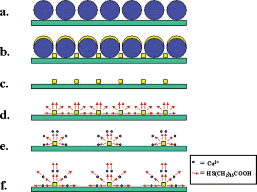
Figure 2. FESEM image of an array of close-packed one-micron polystyrene nanospheres formed by spin-coating the nanosphere solution onto a SiO2 substrate. Scale bar = 10 µm.
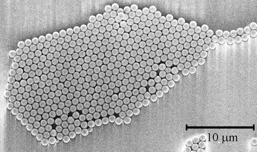
Figure 3. FESEM image of an array of Au/Ti particles formed by evaporating the metals through holes in a hexagonally packed 240 nm nanosphere mask. Particle shadow is formed by the FESEM detector position and is not inherent to the sample. Scale bar = 250 nm.
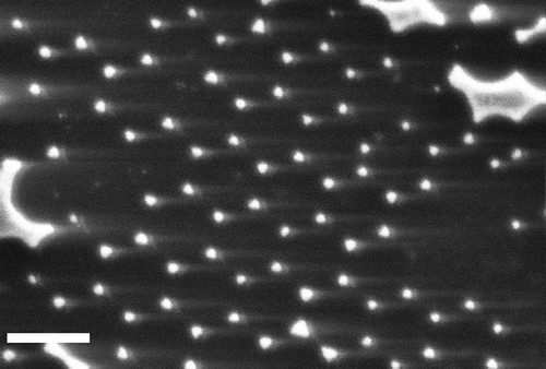
Figure 4. FESEM image of 10 layers of Cu2+ complexed 16-mercaptohexadecanoic molecular layers grown on a gold dot array. The sample was coated with 2 nm evaporated gold to enhance SEM contrast and to stabilize the organic structures that are otherwise sensitive to the electron beam. Nanospheres with diameters of 240 nm were used as a mask for this gold dot arrays. The scale bar indicates 100 nm.
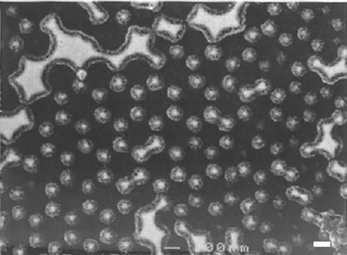
Figure 5. FESEM image of 20 layers of Cu2+ complexed mercapto-alkanoic molecular layers grown on a gold dot array: The sample was coated with 2 nm evaporated gold to enhance SEM contrast and to stabilize the organic structures that are otherwise sensitive to the electron beam. Nanospheres with diameters of 240 nm were used as a mask for this gold dot arrays. The scale bar indicates 100 nm.
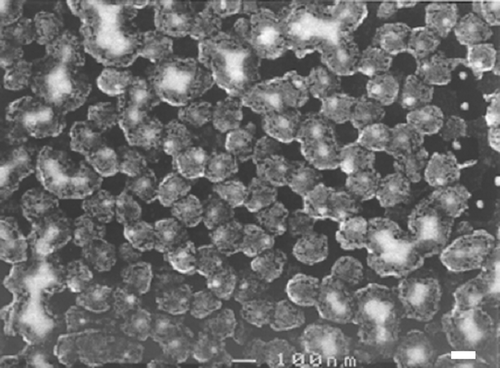
Figure 6. Illustration of the second metal-deposition step and removal of the organic structures: (a) The organic multilayer structure on the original gold-dot array as shown in , (b) gold (with a 2 nm Ti precursor layer) is evaporated on top of the organic layers, and into the gaps between them. In these gaps the gold is deposited directly onto the SiO2/Si surface, (c) the organic layers and the gold on top of it are removed in an organic solvent Citation14, to leave only the original gold structures and the new ‘daughter’ gold structures on the surface. The squares represent the original gold dot structures and the rectangles represent the star-shaped new gold structures as shown in .
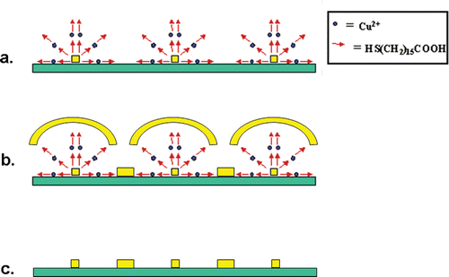
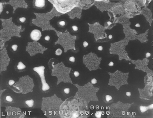
Figure 7. Subsequent gold deposition on the sample shown in , followed by organic layers removal to form an array of star-shaped nanostructures within the original gold-dot array. Scale bar = 100 nm.
2. Experimental section
Suspensions of unfunctionalized polystyrene spheres of diameter 240–1000 nm (Bangs Laboratories) were diluted (1:2) by a 1:400 solution of Triton X-100 (Sigma-Aldrich) in methanol (VWR) Citation9. After dilution, the nanosphere suspensions were spin-coated onto isopropanol-cleaned, oxidized Si wafers with areas between 0.5 cm2 and 2.0 cm2. The nanospheres were deposited using a spin coater (Headway Research Inc., Model CB15) operated at ∼500 rpm for 2 min. Excess fluid at the perimeter of the wafers was wiped dry. A 40 sec O2/Ar reactive ion etching (RIE) was performed (Plasma-Therm 720 RIE, SLR Series) to remove surfactant residues remaining in interstices of the sphere monolayer; this step is crucial to the adhesion of the metal deposited on the SiO2 surface.
The monolayer was then used as a mask ( and , ), first for electron gun evaporation of a 6 nm Ti underlayer, followed by thermal evaporation of a 40–100 nm Au layer (Kurt J. Lesker E-gun/Thermal Evaporator). Subsequent removal of the nanospheres by sonication in CH2Cl2 (J. T. Baker) for 2 min Citation9 left a hexagonal array of ∼40 nm-wide metal particles on the substrate (, ).
Coordinated metal ion-organic multilayers Citation14–18 were adsorbed on the metal dots, by alternate deposition of 16-mercaptohexadecanoic acid (SH-(CH2)15-COOH, Aldrich), 1 mM in ethanol and Cu2+ ions (Cu(ClO4)2, Aldrich), 1 mM in ethanol Citation19. Adsorption times for the organic molecules ranged from 4 h to overnight. Cu2+ adsorption time was 3 min. Samples were rinsed by ethanol and dried under a nitrogen stream between all adsorption steps and after adsorption was completed. Here, 10 or 20 such layers (each layer consists of one organic molecule plus one Cu2+ ion) were adsorbed on different samples (we have successfully used this technique with 3–30 layers in prior work Citation14). The linear growth of the layers was verified using ellipsometry: the thickness of each additional layer grown on gold thin films was measured and was identical to all other layers (2.0 ± 0.2 nm) Citation19. X-ray photoelectron spectroscopy (XPS) measurements were conducted as an independent characterization technique to verify the organic layer contents. The XPS atomic concentrations of the various chemical elements (i.e. C = 84.2%, O = 6.9%, S = 4.7%, Cu = 3.7% [±0.2]) reflect precisely the composition of the layers considering small (<1%) sulfur contaminations that are always present in such samples. 0.5% of Au was found as well, as expected from the underlying gold surface. For FESEM imaging, the samples were coated by 2 nm of evaporated gold. Field emission scanning electron microscope (FESEM) images were taken using a Leica LEO 1530 FESEM and a JEOL JSM-6300F FESEM. For the construction of the gold-star ‘daughter’ structures ( and ) we evaporated ∼2 nm of Ti followed by ∼10 nm of Au on top of the organic structures shown in . This evaporation was followed by dissolution (lift-off) of the organic layers in an organic solvent, as described previously Citation14.
3. Results and discussion
is a scheme showing the various steps required for the build-up of the metal ions/organic nanostructure array. Figures are FESEM images showing the samples at these various process steps. shows an array of 240 nm diameter nanospheres arranged on the Si/SiO2 surface. This regular pattern was formed by self-assembly of the spin-coated spheres. At the junction between every three neighboring spheres, the gap is large enough to allow evaporated gold atoms to penetrate and to reach the underlying Si/SiO2 surface. When gold is evaporated on top of this sphere array, it covers the tops of the spheres and enters into the gaps, as shown in . shows the sample after gold evaporation and subsequent removal of the spheres using sonication. The triangular gold dot array reflects the small junction areas between every three adjacent spheres. The shapes of the gold dots are close to triangular, as expected from such sphere geometry. The size of each gold dot is ∼40 nm which is expected and dictated by the diameter of the nanospheres. This step in the process is illustrated in .
and show the selective assembly of the organic multilayers on the gold dot array. As illustrated in , this growth is conducted by exposing the surface to a solution of the long organic molecules that self-assemble onto the gold forming a monolayer. The sample is then rinsed and inserted in a solution of the Cu2+ ions that serve to link two layers of organic molecules. The sample is rinsed again and placed in the organic molecule solution, and this process is repeated to form the desired number of layers on the surface.
shows a FESEM image of a sample coated with ten metal-ion-complexed organic layers. Ten complexed organic layers are expected to yield 20 nm thick coating since each layer is 2 nm thick. The FESEM image reflects this expected thickness of ca. 20 nm grown off of the gold dots. is a similar image of a different sample coated with 20 layers of the complexed organic molecules. Here the thickness of the layers was ca. 40 nm, corresponding to the length of each molecular layer (2 nm) multiplied by the number of layers formed (20 layers). In this image it can be seen that multilayers grown from adjacent gold patterns reached each other and closed the gap completely. The original gap size of ∼80 nm between two neighboring gold structures was then covered by the two ∼40 nm organic growth areas originating from each dot. In some of these crossing areas, gaps of less than 10 nm appeared to remain, although growth in other areas persisted. This might be attributed to diffusion limitations of molecules into these thin gaps. The gold dots can be seen inside each structure. Note that in the gold dots are not always centered within each structure, yet the organic multilayers followed a periodic array. It might be that the gold array in the imaged area was not totally symmetric prior to molecular adsorption (note irregular spacings between parent structures in some areas of ). Nevertheless, the diffusion limitations of adsorption caused by neighboring growing clusters have the effect of healing this initial asymmetry. The holes (dark) appearing in the images might be areas of incomplete growth between adjacent growing clusters. Structure deformation under the SEM beam is excluded by the evaporation of 2 nm gold layer on top of the structure prior to imaging ( and captions). Imaging of different samples without the 2 nm gold adlayer shows identical structures with lower image contrast.
The growth of the organic layers from a well-defined gold dot array enables direct imaging of the organic multilayer formation in its initial steps. By reducing the dimensions of the gold nucleating centers and by using various functional organic molecules with or without metal ions, a large number of organic nanoparticles can be created. Hybrid inorganic/organic or pure inorganic clusters can be similarly formed Citation20. The organic nanoparticles formed complement the family of inorganic nanoparticles studied to date (see ref. Citation21 and references therein). The fabrication technique demonstrated here can be used to create nucleation centers for studying crystal growth mechanisms. The molecular ruler procedure is highly applicable for creating novel patterned surfaces for optical and electronic devices.
As illustrated in , the process shown above was further used to create more complex structures on the surface. This was done by starting with the nanostructures shown in . The organic layers served as a mask for a second gold deposition step (). Gold deposition was followed by the removal of the entire organic layer structure in an organic solvent () Citation14. The result was an array of star-shaped structures that formed between the original gold dot array. This array is shown in .
The gaps between the stars and the original gold-dot array reflect the area that was previously covered by the organic layers. The second metal deposited is not restricted to gold. Therefore, structures with two different metals can be formed where the two metals are in very close proximity (40 nm in this case). Such two-metal geometries are hard to achieve using conventional lithographic techniques. The shapes and sizes of these ‘daughter’ nanostructures can be controlled easily using organic molecules of various lengths and by choosing the desired number of organic layers deposited.
4. Conclusion
We have shown the controlled uniform growth of organic multilayers from a periodic gold dot array on SiO2 surfaces. This special geometry enables imaging of the metal-organic structure formation in its initial stages. This process can be used to fabricate new organic/metal nanostructures for possible uses in electronic or optical devices. The layer-by-layer growth can yield an isolated organic dot structure on a continuous surface or a continuous organic network exposing only an isolated array of surface dots. The molecular ruler technique enables the formation of novel and complex nanostructure arrays. The fine structure design depends on the initial dot spacing, the length of the organic molecule chosen and on the number of layers grown. Each of these parameters can be easily modified. The combination of NSL and the molecular ruler technique for creating nanostructure arrays is shown to be a very simple fabrication method. It offers great versatility in shape, in structure and in material combination.
Acknowledgements
The authors would like to thank the Penn State Materials Research Institute staff for their help and suggestions. We thank Mark Horn for helpful discussions. We thank Robert Willett for his help with the SEM. This work was funded by AFOSR, DARPA, NSF, ONR and the Intel Research Fund.
References
- Colvin , V . 2001 . From opals to optics: colloidal photonic crystals . MRS Bulletin , 26 : 637
- Chou , SY . 1997 . Patterned magnetic nanostructures and quantized magnetic disks . Proc. IEEE , 85 : 652
- Soong , RK , Bachand , GD , Neves , HP , Olkhovets , AG , Craighead , HG and Montemagno , CD . 2000 . Powering an inorganic nanodevice with a biomolecular motor . Science , 290 : 1555
- Andres , RP , Bielefeld , JD , Henderson , JI , Janes , DB , Kolagunta , VR , Kubiak , CP , Mahoney , W and Osifchin , RG . 1996 . Self assembly at a two-dimensional superlattice of molecularly linked metal clusters . Science , 273 : 1690
- Park , SJ , Lazarides , AA , Mirkin , CA , Brazis , PW , Kannewurf , CR and Letsinger , RL . 2000 . The electrical properties of gold nanoparticle assemblies linked by DNA . Angew. Chem. , 39 : 3845
- Fischer , UC and Zingsheim , HP . 1981 . Submicroscopic pattern replication with visible light . J. Vac. Sci. Technol. , 19 : 881
- Deckman , HW and Dunsmuir , JH . 1982 . Natural lithography . Appl. Phys. Lett. , 41 : 377
- Deckman , HW and Dunsmuir , JH . 1983 . Applications of surface textures produced with natural lithography . J. Vac. Sci. Technol B , 1 : 1109
- Hulteen , JC and Van Duyne , RP . 1995 . Nanosphere lithography: a materials general fabrication process for periodic particle array surfaces . J. Vac. Sci. Technol. A , 13 : 1553
- Haynes , CL , McFarland , AD , Smith , MT , Hulteen , JC and Van Duyne , RP . 2002 . Angle-resolved nanosphere lithography: manipulation of nanoparticle size, shape, and interparticle spacings . J. Phys. Chem. B , 106 : 1898
- Haynes , CL and Van Duyne , RP . 2001 . Nanosphere lithography: a versatile nanofabrication tool for studies of size-dependent nanoparticle optics . J. Phys. Chem. B , 105 : 5599
- Jensen , TR , Malinsky , MD , Haynes , CL and Van Duyne , RP . 2000 . Nanosphere lithography: tunable localized surface plasmon resonance spectra of silver nanoparticles . J. Phys. Chem. B , 104 : 10549
- Boneberg , J , Burmeister , F , Schafle , C , Leiderer , P , Reim , D , Fery , A and Herminghaus , S . 1997 . The formation of nano-dot and nano-ring structures in colloidal monolayer lithography . Langmuir , 13 : 7080
- Hatzor , A and Weiss , PS . 2001 . Molecular rulers for scaling down nanostructures . Science , 291 : 1019
- Anderson , ME , Smith , RK , Donhauser , ZJ , Hatzor , A , Lewis , PA , Tan , LP , Tanaka , H , Horn , MW and Weiss , PS . 2002 . Exploiting intermolecular interactions and self-assembly for ultrahigh resolution nanolithography . J. Vac. Sci. Technol. B , 20 : 2739
- Anderson , ME , Tan , LP , Tanaka , H , Mihok , M , Lee , H , Horn , MW and Weiss , PS . 2003 . Advances in nanolithography using molecular rulers . J. Vac. Sci. Technol. B , 21 : 3116
- Tanaka , H , Anderson , ME , Horn , MW and Weiss , PS . 2004 . Position-selected molecular ruler . Jpn. J. Appl. Phys. , 43 : L950
- Anderson , ME , Mihok , M , Tanaka , H , Tan , L-P , Horn , MW , McCarty , GS and Weiss , PS . 2006 . Hybrid approaches to nanolithography: photolithographic structures with precise, controllable nanometer-scale spacings created by molecular rulers . Adv. Mat. , 18 : 1020
- Evans , SD , Ulman , A , Goppert-Berarducci , KE and Gerenser , JL . 1991 . Self-assembled multilayers of ω-mercaptoalkanoic acids: selective ionic interactions . J. Am. Chem. Soc. , 113 : 5866
- Guo , S , Konopny , L , Popovitz-Biro , R , Cohen , H , Porteanu , H , Lifshitz , E and Lahav , M . 1999 . Thioalkanoates as site-directing nucleating centers for the preparation of patterns of CdS nanoparticles within 3-D crystals and LB films of Cd alkanoates . J. Am. Chem. Soc. , 121 : 9589
- Grieve , K , Mulvaney , P and Grieser , F . 2000 . Synthesis and electronic properties of semiconductor nanoparticles quantum dots . Curr. Opin. Colloid & Interface Sci. , 5 : 168