Abstract
The unique electronic, mechanical and chemical properties of carbon nanotubes make them most promising candidates for the building blocks of molecular-scale machines, and nanoelectronic devices. On the other hand, highly hydrophobic films are being actively considered in silicon based micro-electromechanical systems, nanotechnology based devices, optoelectronic devices, or biomedical devices to reduce adhesion that may be encountered during wet processing. In order to fill the gap, and fulfill the requirements, it could be proved that morphological changes in the nanometer range influences the water contact angles and their hysteresis of low-surface energy materials. Thin films of fluorine based block co-polymer itself forms nano-hemispheres (similar to lotus leaf) at and above 100°C favoring an increase in the water contact angle from 122° (25°C) to 138° (400°C). The structural, optical, mechanical and hydrophobic properties of fluorine based block co-polymer are also discussed. By applying nanolayered (5 nm) fluorine-based block co-polymer film on a vertically aligned carbon nanotubes (CNT) morphology with a certain roughness, the advancing contact angle for water on fluoro-based polymer film on a nearly atomically flat Si wafer increased from 122° to 138° (close to super hydrophobicity) and 150° on the rough asparagus-like structure of CNT has been observed.
1. Introduction
It is well known that the hydrophobicity of a surface is strongly affected by the chemical composition and topographical appearance. Considering only the chemical factor, contact angles of around 120° can be obtained for materials with the lowest surface energy (6.7 mJ/m2 for a surface with regularly aligned closer-hexagonal packed –CF3 groups). For achieving higher contact angles (super hydrophobicity), a certain topography is required. For the topographical modification of low-surface energy materials, in the last years two main approaches have been investigated. The first approach, considering the structuring or texturing of the material itself during or after depositing on a smooth substrate through, e.g. varying the deposition conditions Citation1, post treatment with ion or electron beam, and plasma etching Citation2. In other cases, the low energy materials were deposited on substrate with certain structure or texture, which were obtained by methods like embossing or laser ablation Citation3, photolithography Citation4 or deposition of rough interlayer by thin film technology. It was proved that, by combining the chemical structure (by using sol--gel technique) with nano-topography (by using sputtering), one could achieve super hydrophobicity Citation5.
Many deposition techniques including physical vapor deposition (PVD), chemical vapor deposition (CVD) or plasma polymerization, have been used to produce hydrophobic coatings on glass, silicon and other metallic substrates. Unlike PVD, CVD, or plasma polymerization techniques, with the sol--gel technique it is possible to modify the surface of any material (e.g. glass, metal, polymers) with organic polymers. This process is cost effective with easy operation at low or even at ambient temperature. One main advantage of the process is the possibility to coat three-dimensional substrates (or irregular geometries) with high homogeneity in film thickness and good adhesion.
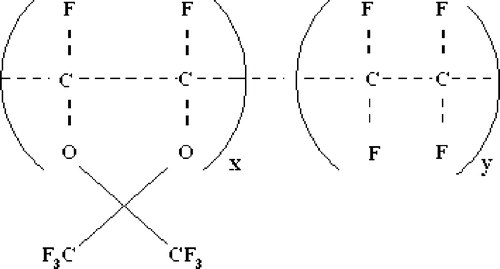
In the present work, a clean, and economic process is introduced to prepare temperature-resistant, hydrophobic thin films on Si(100) and vertically aligned CNT previously deposited on Ni nanoparticles on SiO2/Si substrates. Keeping in view the necessity of the hydrophobicity on nanoelectronics made from carbon nanotubes, an attempt has been given to spin coat a nanolayer (5 nm) of hydrophobic fluorine containing block-co-polymer poly[4,5-difluoro-2,2-bis(trifluoromethyl)-(1,3-dioxole)-co-tetrafluoroethylene] here after called (TFD-co-TFE) on to bare Si(100) substrates as well as previously grown carbon nanotubes on SiO2/Si substrates. Films deposited on quartz, glass surfaces Citation6 and polished AISI 440C steel surfaces Citation7 and their structural, chemical characterization, wettability properties have been reported. The basis of this work is the use of fluorine containing block-co-polymer namely TFD-co-TFE. Compared to perfluoroalkylsilane or hexamethyldisilazane, TFD-co-TFE exhibits higher mechanical strength, chemical durability, and temperature stability. The importance of the compound is the stability to high temperatures up to 400°C, which could be attributed to the carbon--oxygen link of the fluorine containing block-co-polymer structure as depicted in .
Figure 1. Structure of the fluorine-based block-co-polymer used as a precursor for the preparation of TFD-co-TFE films by wet chemical spin coating process
Sol--gel thin films based on this compound have been prepared by a spin coating technique followed by annealing at low temperatures. It was observed that as the annealing temperature increased from 100°C to 400°C nano-hemisphere-like structures were formed on the film surfaces of TFD-co-TFE coated on Si(100).
2. Experimental procedure
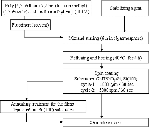
Calculated quantities (0.1 M) of TFD-co-TFE (amorphous copolymer: 65 mole% dioxole, Tg: 160°C) were dissolved in special fluorinated solvent (Fluorinert FC-70) in a 100 ml round bottom flask. Both reagents were obtained from FLUKA Chemicals and used without further purification. To the above solution a few drops of stabilizing agent were added and stirred at room temperature for about 6 hours in nitrogen atmosphere to prevent particle contamination. The contents were refluxed at 40°C for 4 h. The final solution was filtered in order to remove any particulates formed during the process. The obtained filtered stock solution was used for spin coating the substrates. A schematic flow chart diagram for the preparation of the hydrophobic thin films by sol--gel spin coating technique is shown in .
Figure 2. Flow chart for the preparation and deposition of TFD-co-TFE thin films by wet chemical spin coating process
Polished Si(100) substrates and CNT grown on Ni nanoparticles on Si substrates with surface roughness Ra = 1.5 nm and 36 nm, respectively have been used in the present study. The deposition parameters for the growth of vertically alighned CNT on Ni nanoparticles on Si substrates by chemical vapor deposition technique were described elsewhere Citation8. Prior to spin coating, Si(100) substrates were rinsed with isopropanol and then placed in a trough containing isopropanol and subjected to ultrasonic cleaning for 15 min in order to remove any organic matter and dust particles present on the surface. Afterwards the substrates were again rinsed with isopropanol and then blown dry with high purity nitrogen gas (99.95%).
The clean substrates were immediately placed in the spin coating chamber. Using a 50 microliters pipette, 10 microliters of the stock solution was placed on the surface of the substrate and spun at 1000 rpm speed for 30 sec (cycle-1) to spread the solution over the entire surface of the substrate. This step was followed by 3000 rpm for 30 sec (cycle-2) in order to evaporate the solvent. The steps consisting of cycle-1 and cycle-2 were repeated 10 times for the Si(100) substrates and once for CNT/SiO2/Si substrates in order to get 50 nm thickness and 5–8 nm nanolayer thickness, respectively. At the end, the obtained xerogel films deposited on Si(100) were subjected to annealing for 1 hour at different temperatures ranging from 100°C to 400°C in argon atmosphere.
The microstructure, elemental composition, and surface topography of the TFD-co-TFE xerogel films as well as annealed thin films were characterized by employing transmission electron microscopy (TEM), energy dispersive X-ray (EDX) analysis, transmission electron diffraction (TED), and atomic force microscopy (AFM) techniques, respectively.
3. Results and discussions
3.1. Scanning electron microscopy
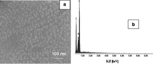
SEM images and the corresponding energy dispersive X-ray (EDX) spectra of the TFD-co-TFE film deposited on Si(100) at room temperature and annealed at 400°C for 1 h in argon atmosphere are shown in and , respectively. As deposited (xerogel) films were uniform with flat and smooth structure. It became difficult to take the SEM images because of the interaction of the high electron beam on the sample, which caused the film to leave with a small hole. No morphological changes in the surface were observed for the annealed samples at other temperatures except in the growth of the nano-hemisphere-like structures. and represent SEM--EDX spectra of the TFD-co-TFE film on Si(100) for both xerogel film and xerogel film annealed for 1 h at 400°C in an argon atmosphere. The X-ray pattern confirms the presence of carbon and fluorine along with oxygen content in the films. The weight percent of the C, F and O in the film were 40.2 wt%, 42.3 wt% and 17.5 wt%, respectively. Similar behavior was also observed for the annealed samples.
Figure 3. SEM image and EDX spectrum of TFD-co-TFE film deposited on Si(100) at room temperature by sol--gel spin coating process
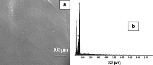
Figure 4. SEM image and EDX spectrum of TFD-co-TFE film deposited on Si(100) by sol--gel spin coating process and annealed at 400°C for 1 h
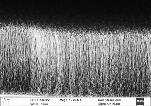
Vertically aligned carbon nanotube structure on Ni nanoparticles (as nucleating seeds) as deposited on SiO2/Si substrate grown at substrate temperature 50°C is shown in the . It is evident from the figure that the growth of carbon nanotubes is rough and creates an asparagus-like structure. More details of the experimental parameters for the deposition of vertically aligned carbon nanotubes have been reported elsewhere Citation8.
Figure 5. SEM image of vertically aligned CNT on Ni nanoparticles on SiO2/Si substrate grown at 750°C by radio frequency pulsed plasma chemical vapor deposition technique
3.2. Atomic force microscopy
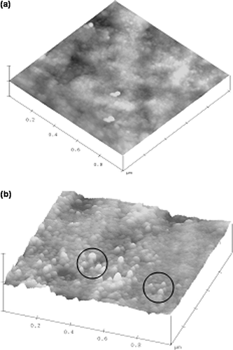
represent the topographical AFM images of the TFD-co-TFE films deposited on Si(100) substrates for both xerogel film and xerogel film annealed for 1 h at 400°C in an argon atmosphere. The xerogel films have exhibited a flat like structure with little formation of nano-hemisphere like structures as indicated by the white circles (). As the annealing temperature was increased from 100°C to 400°C, the growth of nano-hemisphere-like structures was increased as shown in the , indicated by white circles. The roughness of the films has been measured by AFM technique. The roughness of the films (Ra) deposited on Si(100) substrates has changed with annealing temperature from 8 ± 1 nm for xerogel film to 32 ± 1 nm for the film annealed at 400°C. The growth size of the nano-hemispheres increased from 6 ± 1 nm for xerogel film to 26 ± 1 nm for film annealed at 400°C.
Figure 6. AFM topographical images of TFD-co-TFE thin films on Si(100) substrate by sol--gel spin coating process (a) As deposited (xerogel) film and (b) xerogel film annealed at 400°C/1 h (scan area 1 µm × l µm, Z axis = 100 nm)
3.3. Hydrophobicity
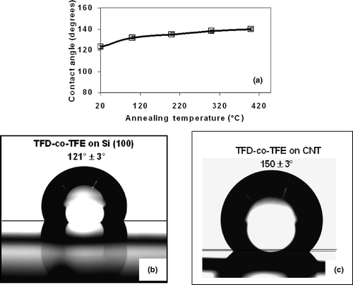
Contact angle of the films deposited at room temperature and annealed at different temperatures as well as substrate heated at various temperatures have been measured by spheroidal segment method using a contact angle measurement system (Circular Curve Fit Option). The contact angle, θ, was derived from advancing contact angle, θa, and reducing contact angle θb, by the following equation: cos θ = (θa + θb)/2 or [(γSV − γLV)/γLS], where γSV, γLV, and γLS are free energies of solid--vapor, liquid--vapor and liquid--solid interfaces, respectively ().
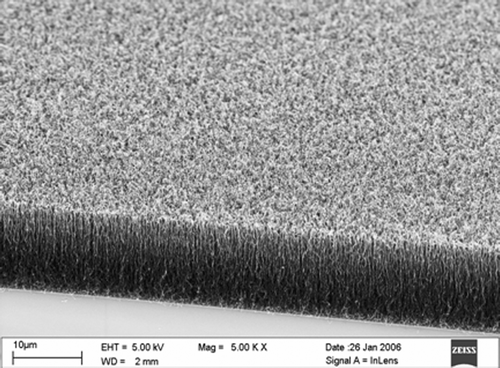
Figure 7. SEM planar view of the vertically aligned CNT coated with hydrophobic ultra thin film (5 nm) (TFD-co-TFE)
Water contact angle versus annealing temperature for the TFD-co-TFE films on Si (100) substrates are presented in . From , it was evident that TFD-co-TFE films on Si(100) as deposited show a water contact angle of 122° and as the annealing temperature increased from 100°C to 400°C the contact angle was increased from 122° to 138°. This could be due to the growth of nano-hemisphere like structures causing an increased surface roughness at 100°C and above. The room temperature water contact angles of TFD-co-TFE film deposited on Si(100) and CNT/SiO2/Si were 123° and 150° as shown in , respectively.
Figure 8. (a) Water contact angles vs. annealing temperatures of TFD-co-TFE films deposited on Si(100). Water droplet picture taken during measurement at room temperature (b) TFD-co-TFE film coated on Si(100) and (c) TFD-co TFE film coated on CNT/SiO2/Si
4. Conclusions
Poly[4,5-difluoro-2,2-bis(trifluoromethyl)-(1,3-dioxole)-co-tetrafluoroethylene] (TFD-co-TFE) films have been deposited by sol--gel spin coating technique on Si(100) and CNT previous grown on Ni nanoparticles on SiO2/Si substrates. The as deposited xerogel films on Si(100) have been subjected to annealing for 1 h at different temperatures ranging from 100°C to 400°C in an argon atmosphere. SEM--EDX spectra confirmed the presence of carbon (∼41 wt%), fluorine (∼41 wt%) and oxygen (~18 wt%) in the deposited and annealed films. AFM topographical images revealed the formation of nano-hemisphere-like structures with increasing annealing temperatures. The size of the nano-hemispheres increased from 8 nm for xerogel film to 28 nm for film annealed at 400°C on Si(100). The room temperature water contact angles of TFD-co-TFE film deposited on Si(100) and CNT/SiO2/Si were 123° and 150°, respectively.
References
- Cicala , G , Milella , A , Palumbo , F , Favia , P and d’Agostino , R . 2003 . Morphological and structural study of plasma deposited fluorocarbon films at different thicknesses . Diam. Relat. Mater. , 12 : 2020
- Inoue , Y , Aoshimura , Y , Ikeda , Y and Kohno , A . 2000 . Ultra-hydrophobic fluorine polymer by Ar-ion bombardment . Colloid. Surface B. , 19 : 257
- Sugimura , H , Ushiyama , K , Hozumi , A and Takai , O . 2000 . Micropatterning of alkyl- and fluoroalkylsilane self-assembled monolayers using vacuum ultraviolet light . Langmuir , 16 : 885
- Uelzen , T and Muller , J . 2003 . Wettability enhancement by rough surfaces generated by thin film technology . Thin Solid Films , 434 : 311
- Gerbig , Y , Phani , AR and Haefke , H . 2005 . Influence of nanoscale topography on the hydrophobicity of fluoro-based polymer thin films . Appl. Surf. Sci. , 242 : 251
- Phani , AR , Passacantando , M and Santucci , S . 2006 . Structural, compositional, thermal resistant and hydro-oleophobic properties of fluorine based block co-polymer films on quartz substrate by wet chemical process . J. Phys. Chem. Solids , 67/68 : 1703
- Phani , AR . 2006 . Structural, morphological, wettability and thermal resistance properties of hydro-oleophobic thin films prepared by a wet chemical process. . Appl. Surf. Sci. , 253 : 1873 – 1881 .
- Passacantando , M , Grossi , V and Santucci , S . 2007 . J. Appl. Phys , in press