Abstract
In this paper, we present two nanoscale architectures with full spin-wave interconnectivity. The first architecture is a fully interconnected cluster in which each node can simultaneously broadcast to all other nodes, and can concurrently receive and process multiple data. The second architecture is a crossbar interconnected with ferromagnetic buses that, while requiring the same number of switches and buses as the standard crossbar, is capable of simultaneously transmitting multiple waves at different frequencies on each of the spin-wave buses. The significance of these designs is that the communication between the nodes can be done in constant time, which is a noteworthy improvement considering the Ω(log N) lower-bound on the time delay for implementing such networks in VLSI using traditional electrical interconnects. In these architectures, unlike traditional spin-based architectures that transmit charge, the information is encoded into the phase of spin waves. As a result of this, the presented nanoscale designs may have low power consumption.
1. Introduction
During the past several decades, many multi-processor VLSI chips have been proposed with the goal of obtaining optimal speed-ups in minimal area. Nevertheless, the desired speed-ups are not always realizable due to certain inherent limits in the VLSI technology. For example, the VLSI area of a fully interconnected network of multiprocessors on a chip, in which each of the computing nodes can send (or receive) data to (or from) all the other nodes directly and in constant time, is in the order of O(N 4), which would be unreasonably large to implement. Furthermore, the implementation of such an organization will require having nodes with O(N) fan-in fan-out, which also is not practical in VLSI. If constant degree nodes were to be used instead, there would be an Ω(log N) intercommunication delay lower-bound in realizing such a network in VLSI using electrical interconnects. The replacement of electrical wires with free-space optical interconnects, though, can significantly improve the VLSI area and fan-in fan-out limitations Citation1. However, electro-optical designs have their own challenges, especially with respect to switching issues Citation2.
Another alternative for reducing the VLSI area requirement is to use nanoscale architectures. Several methods have been proposed during the past few years for the design of such chips. Among them are designs that have single electron transistors, molecular switches, quantum-dots, carbon nanotubes, and spins Citation3. In traditional spin-based devices, information is stored into spins as a spin orientation (along with or opposite to the external magnetic field). The spins, attached to carriers, transfer information from one spin-based device to another through a conducting wire. We propose to use spin-wave-based devices in which the wave transmits the information without any charge transfer.
In this paper, we present two nanoscale architectures with full spin-wave interconnectivity. The first architecture is a fully interconnected cluster in which each node can simultaneously broadcast to all other nodes, and can concurrently receive and process multiple data. The second architecture is a crossbar interconnected with ferromagnetic buses that while requiring the same number of switches and buses as the standard crossbar, is capable of simultaneously transmitting multiple waves at different frequencies on each of the spin-wave buses. The significance of these designs is that the communication between the nodes can be done in constant time, which is a noteworthy improvement considering the Ω(log N) lower-bound on the time delay for implementing such networks in VLSI using traditional electrical interconnects. Moreover, these fully interconnected architectures can be laid out in area O(N 2) as opposed to O(N 4), and of course the unit of area is in order of tens of nanometres as opposed to the standard micron technology that is currently in use. In these architectures, information is encoded into the phase of spin waves, and charge is not transmitted. As a result of this, power consumption may be significantly reduced in these architectures.
The rest of the paper is organized as follows: In the next section, we present our proposed spin-wave-based architectures. In section 3, we show our experimental results. Our conclusion and future work is presented in section 4.
2. The fully interconnected architectures
The use of spin waves for computation is an entirely new idea. The first computational architecture to utilize spin waves for massive entanglement of distant spin-based qubits in a quantum computer was described in earlier publications Citation4, Citation5. Later, in another publication Citation6, and here, too, spin waves are used for both information transmission and information processing. We employ the classical type of computing as opposed to quantum, and the architectures presented can operate at room temperature as shown later in this paper.
In this section, we first give a brief introduction to spin waves, and then present our two proposed nanoscale architectures with full spin-wave interconnectivity: the fully interconnected spin-wave cluster, and the spin-wave crossbar.
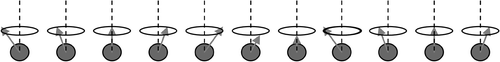
Electron spin produces a magnetic moment, and if a magnetic field is applied, then this spin moment will precess about the field. A collection of such spin precessions is a spin wave Citation7, as shown in . The magnitude of the spin wave is determined by the precession angle. Typically, the speed of the spin wave is 104 metres per second. According to our current experimental results presented later in this paper, the switching frequency is in the order of GHz, but up to the order of THz is possible. Attenuation of the spin wave is around 50 microns, which makes it a suitable candidate for ‘nano’-scale communication.
Figure 1. A spin wave: a collection of precession of electron magnetic moment about a magnetic field.
2.1. The fully interconnected spin-wave cluster
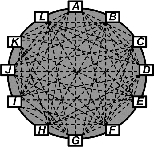
This architecture is a fully interconnected cluster in which each node can simultaneously broadcast to all other nodes, and can concurrently receive and process multiple data. shows the top view of the architecture in which the N computing nodes are placed around a circle on a magnetic film. The area requirement of this architecture is O(N 2) as opposed to the O(N 4) area requirement if electrical interconnects were to be used. We should also note that all the distances in this architecture are in nanoscale. Also, unlike electrical interconnection networks, in which only one transmission can be done at a time, here multiple simultaneous permutations are possible by transmitting the spin waves over different frequencies. The information is coded into the phase of the spin waves in the sender and is detected by the receivers. In addition, within each frequency, data can be sent to one or more other nodes from each node.
Figure 2. The top view of the architecture with full spin-wave interconnectivity.
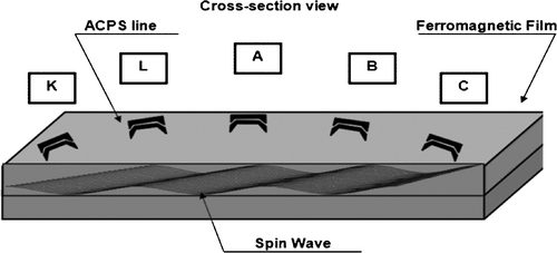
shows the cross-view of the layout of this architecture on a semiconductor chip. Each node is an Asymmetric Co-Planar Strip (ACPS) line (described later in the implementation section), which can be used as a sender or receiver at each point of time. In the following, we present a brief discussion about the placement of nodes and the communication mechanisms among them.
Figure 3. Cross-section view of the architecture with full spin-wave interconnectivity.
2.1.1. Placement of the nodes
Normally, in architectures where the phases of the waves are the means of information transmission, the exact location of the nodes with respect to the size of topology is an important design issue. The distance between the sender and receiver has to be at a length that is a multiple of the wavelength; otherwise the receiver might receive the wave with a π radian phase-shift, which is a ‘0’ instead of a ‘1’ or vice versa. However, in our design, this is not an issue because the wavelengths of spin waves are considerably larger than the distance between the nodes. The speed of spin waves is around 105 m/s. Assuming the input frequency range of 1–10 GHz (as in our experiment), the wavelength will be in the order of 10−4–10−5 m, while the distances are nanoscale or 10−8 m. In other words, the wavelengths of the spin waves are some orders of magnitude greater than the distances between the nodes. Therefore, all the nodes receive the same phase regardless of their location, and there is no need to place the nodes in specific distance relative to the other ones Citation8.
2.1.2. Communication among the nodes
In this architecture, as shown in the top view, each node can broadcast to all other nodes simultaneously. For instance, node A can broadcast to all the other nodes. This requires that the receiving frequencies of all the nodes be tuned to the same frequency as the transmitting frequency of node A. Similarly, a node can receive and process multiple data simultaneously. For instance, node G can receive multiple data simultaneously from other nodes. In this case, the requirement is that all the nodes should transmit at the same frequency as the receiving frequency at which node G is tuned.
To distinguish the data being transmitted to different nodes, transmissions are done at distinct frequencies. In a way, this is similar to having various radio stations, where each broadcasts at a different frequency. To listen to a specific station, one tunes to the corresponding frequency. Here, similarly, each node can broadcast or receive at a specific frequency. Furthermore, at a given frequency, a node can listen to multiple waves simultaneously. Using the superposition property of waves, it can compute the sum of all waves destined to it.
In addition to the transmissions at different frequencies, all nodes in this architecture can work on the same frequency in a broadcast mode, or they can be directed to specific locations using phased array techniques Citation9. It is also possible to combine the phased array technique with multiple frequencies. This way, for each frequency, some of the waves are only transmitted to desirable directions and are received by the intended sources.
2.1.3. Data detection at the nodes
In our architecture, the communication is done via spin waves but the computation is done electronically. When mapping an algorithm to this architecture, one should take into consideration the fact that once the spin waves are detected by the receiver ACPS lines, the transmitted data can either be digitized or they can be left analogue.
First, the input information is coded into the polarity of the voltage pulse applied to the edge ACPS lines (for example, V input = +1 V corresponds to the logic state 1, and V input = −1 V corresponds to the logic state 0). Next, in order to detect the output signal V ind, we use the time-resolved inductive voltage measurement.
In analogue detection mode, the ACPS line detects the inductive voltage produced by the superposition of multiple waves. For example, if 10 waves are sending a ‘1’, then their analogue sum through their cumulative amplitude is computed instantly as 10. Also, this property can be used to compute logical functions as described previously. In digital detection mode, this value is digitized to just a ‘1’, and then the computations are continued digitally.
It is possible to realize different logic gates AND, OR, and NOT controlling the relative phase of the spin waves. The voltage measured in the output port is compared to a reference voltage to determine logic state 1 or 0. This measurement is performed at the moment of spin-wave packet arrival to the detecting ACPS line area.
2.2. The crossbar with spin-wave buses
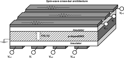
Crossbars are attractive architectures because they can realize any permutations of N inputs to N outputs. However, their main shortcoming is that N 2 switches are used to transmit only N pairs of data. The architecture described here, while requiring the same number of switches as standard crossbars, is capable of transmitting N 2 data elements. This is due to the fact that each spin-wave bus is capable of carrying multiple waves at any given instance of time. Therefore, each of the N inputs in parallel can essentially broadcast its data to all of the N outputs. In other words, using this type of architecture, it would be possible to efficiently realize those types of computations that require high level of interconnectivity. Also, as compared to molecular nanoscale crossbars, this design is fault tolerant because if there is a failure in one of the N channels, other channels can be used to transmit the data. This is possible because all the channels are accessible by all the ports and each channel can handle multiple data.
An example of the proposed spin-wave crossbar architecture is shown in . Note that a set of column spin-wave buses on the bottom and a set of row spin-wave buses on the top are connected via the vertical spin-wave switches presented below. The switches can be set at GHz speed to direct the data to desired paths. Each switch can be activated by alternating the bias of the corresponding column and row contacts Citation10.
Figure 4. Crossbar with spin-wave buses.
In , the cross-section of the spin-wave switch is shown, which resembles the cross-section of a metal–insulator–diluted magnetic semiconductor structure used for the experimental study of the effect of hole-mediated ferromagnetism in another publication Citation11. There, a ferromagnetic film is divided by a region of diluted magnetic semiconductor (DMS), and it is used as a magnetic channel. The magnetic phase is controlled by the applied electric field via the effect of hole-mediated ferromagnetism Citation11. A negative gate bias increases the hole concentration in the DMS region, resulting in the paramagnetic-to-ferromagnetic transition, whereas a positive bias has an opposite effect as shown in . The cross-section of the spin-wave switch is shown in . As shown, the ferromagnetic film is divided by the DMS cell. Spin waves can propagate through the DMS cell only if it is in the ferromagnetic phase. In the ferromagnetic phase (‘on’ state) the switch transmits spin waves, while in the paramagnetic state (‘off’ state) it reflects any incoming spin waves.
Figure 5. A spin-wave switch design.

The same structure of the spin-wave switch based on the effect of hole-mediated ferromagnetism may be used for the vertical integration of the spin-wave buses. In , we have schematically shown two vertically separated ferromagnetic films with the DMS cell in the place of intersection. In this structure, the switch serves as a connector between two spin-wave buses. At the negative applied bias (ferromagnetic phase), the switch provides coupling between the spins in the ferromagnetic films. At the positive bias (paramagnetic phase), there is no coupling between the films. The use of the spin-wave switches for vertical integration makes possible array-based architectures similar to that proposed for the array of nanowires Citation12.
When mapping an algorithm to this architecture, one should take into consideration the fact that two different types of data detections are possible at the nodes. Once the spin waves are detected by the receiver ACPS lines, the transmitted data can either be digitized or they can be left analogue as explained above in the case of fully interconnected spin-wave clusters.
The proposed spin-wave crossbar architecture has two key advantages: (i) as briefly noted above, there is no strict requirement on the exclusive use of the buses; and (ii) signal information can be encoded in the phase of the propagating spin wave rather than in the number of electrons to be transmitted via conducting wires. As is shown, there is a common p-doped DMS layer for the whole structure. The magnetic phase in every region is controlled by the hole concentration. Using conducting ferromagnetic films (NiFe, for example), it is possible to control the hole distribution along the structure by the applied electric field. The hole concentration is high when both the top and the bottom ferromagnetic films are biased by a negative voltage. There is a self-alignment mechanism that makes the proposed structure tolerant to structure imperfections.
3. Implementations of the architectures
While the architectures presented above have not yet been fully implemented, we have some preliminary experimental results based on a simple prototype that we built in our nano lab at UCLA. The significant point about our experimental results is that the architectures are operable at room temperature and currently have GHz switching speed. In the following, we show our prototype and experimental results, along with a theoretical discussion explaining the operation of the prototype.
3.1. Our prototype and experimental results
Spin waves have been attracting scientific interest for a long time, but only recently were there several experimental types of projects devoted to the problem of spin-wave detection using the inductive voltage measurement techniqu Citation13, Citation14. The results indicate that spin-wave packets propagating in a 100 nanometre thick ferromagnetic film may produce an inductive voltage in the order of several mV, suitable for experimental detection Citation14. The inductive voltage measurement technique appears to be one of the most convenient physical methods for spin-wave detection and integration in a semiconductor platform.
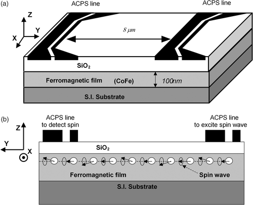
In the ideal case, spin waves can be used to provide an ‘LC’ coupling of devices, without dissipative resistance. With the spin-wave concept, the spin rotates as a propagating wave and there is no particle (electron/hole) transport Citation14. In , we have schematically shown the prototype of the spin-wave-based logic device structure being built at our nano lab. The core of the structure consists of a 100 nm-thick CoFe film deposited on a silicon substrate. There are two asymmetric coplanar strip (ACPS) transmission lines on the top of the structure. The distance between the lines is 8 µm. The lines and the ferromagnetic layer are isolated by a 300 nm silicon oxide layer. The dimensions of the ACPS lines are adjusted to match 50 Ω of the external coaxial cable. One of the ACPS lines (shown on the right) is used for spin-wave excitation. Hereafter, we will refer to this ACPS line as the ‘excitation’ line. A voltage pulse applied to the excitation line produces a magnetic field and excites a spin wave (spin-wave packet) in the ferromagnetic layer. Being excited, the spin wave propagates through the ferromagnetic film. The other ACPS line (shown on the left) is used to detect the inductive voltage signal produced by the propagating spin wave. Hereafter, we will refer to this line as the ‘detection’ line.
Figure 6. Prototype of the logic device structure.
In , we present the experimental data on spin-wave detection by the time-resolved inductive voltage measurement technique Citation15. The dashed line depicts the voltage pulse applied to the excitation line. The pulse characteristics are as follows: pulse amplitude 24.5 V; rising time 1.2 ns; and pulse length 20 ns. The solid line depicts the inductive voltage signal detected by the detection line. One can see the inductive voltage oscillation at the detection line caused by the inductive coupling via the spin waves. The output voltage signal has maximum pulse amplitude 26 mV, and the period of oscillation is 9 ns.
Figure 7. Experimental data on spin-wave detection.
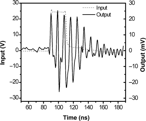
These experimental data illustrate the possibility of signal transmission by spin waves over micrometre range distances. The attenuation time is about 20 ns, and the signal-to-noise ratio is satisfactory (at least for 8 µm propagation distance). We would like to stress that the utilization of spin waves is prominent for short-range in-chip communication. There are several important issues that require additional consideration: (i) power dissipation in the spin-wave bus; and (ii) signal gain. In principle, the energy per spin wave can be scaled down to several kT, to be just above the thermal noise level. On the other hand, in order to compensate for the damping of spin waves, one needs to include an amplification mechanism (gain). One of the possible gain mechanisms may be parametric spin-wave amplification, which has been experimentally demonstrated Citation16.
3.2. The principle of operation
In order to illustrate the principle of operation, we consider the propagation of a spin wave excited by an ACPS transmission line. The spin dynamics can be described using the Landau–Lifshitz equation as follows:
In , we have shown two ACPS lines, one as input and one output. If we add another ACPS line, it can be used as a second input port. Each of the input devices (ACPS lines) excites a spin-wave packet consisting of a Gaussian distribution of wave vectors that is 2/δ in width and centred about k 0. The wave packet propagates along with the y direction and can be described with one magnetization component My as follows:
Figure 8. Numerical simulations results: propagation of a spin-wave packet.
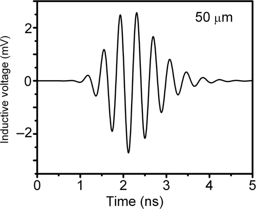
The distance between the excitation point and the point of observation is 50 µm. The spin waves produce a perturbation in spin orientation perpendicular to the direction of magnetization, whose amplitude is much less than the saturation magnetization |My |/Ms ≪ 1.
Next, we consider the combined effect of spin-wave packets produced by two input devices. We assume that each of the input devices generates a spin-wave packet, which is described by equation (Equation3). The amplitudes of the input signals are the same, while the relative phase between the signals can be controlled, for example, by the polarity of the applied current pulses. The current pulses having the same polarity produce local magnetic fields oriented in the same direction, so the generated spin-wave packets have the same initial phase (φ1 = φ2). In the other case, when the current pulses have different polarity, the produced spin-wave packets have relative phase difference (φ1 − φ2 = π).
In order to find the magnetization change caused by two spin-wave packets, we calculated the resultant magnetization as a superposition of waves of the same frequency from each packet:
Figure 9. Numerical simulations results: output of two spin-wave packets.
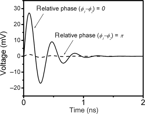
The results of simulations illustrate the output of the prototype logic device described above. As shown in , the amplitude of the inductive voltage is maximum when the spin-wave packets are coming in phase. In the other case, the waves from two packets compensate each other and produce inductive voltage of much less amplitude.
4. Future directions and conclusion
As mentioned in section 2, the attenuation of a spin wave is about 50 microns. In order to overcome this size limitation, we propose using a hierarchical multi-scale architecture, which will embody the spin-wave modules described above.
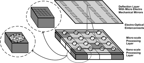
The proposed architecture will be based on the Optical Reconfigurable Mesh (ORM) architecture Citation18, which consists of three layers: the deflection layer, the microscale processing layer, and the nanoscale processing layer. In this architecture, the deflection layer consists of N 2 deflecting units, while the microscale processing layer consists of N 2 processing units. Here each processing unit will be connected to a fully connected nanoscale module at the nanoscale processing layer. The nanoscale module can be either the spin-wave crossbar or the spin-wave cluster explained previously. Each deflecting unit consists of one fixed and one reconfigurable mirror as well as a unit to control the direction of the reconfigurable mirror according to the address sent to it. The processing units at the microscale layer have optical receiver and transmitters as well as regular switches. They are interconnected as a standard reconfigurable mesh and can also intercommunicate optically using the deflection layer.
Data at the microscale processing module level can be routed in three different ways: electrical routing through electrical buses, optical routing via free-space optical interconnections, and electro-optical routing that uses electrical and optical free-space connections to allow a complete connection among N processors Citation19. The nanoscale computing modules are interconnected using spin waves, and at the higher microscale level they are interconnected electro-optically as shown in . This architecture presents one of the many ways in which the spin-wave nanoscale modules introduced here can be integrated into chips. The following are a few concluding remarks about the work we presented in this paper.
Figure 10. The hierarchical architecture with fully interconnected clusters or crossbars in the computing layer.
Two nanoscale architectures with full spin-wave interconnectivity were presented that are operable at room temperature. In the first one, the fully interconnected spin-wave cluster, each node can simultaneously broadcast to all other nodes, and can concurrently receive and process multiple data. The second one, the spin-wave crossbar, is capable of simultaneously transmitting multiple waves at different frequencies on each of the spin-wave buses.
Both of these designs allow nodes to intercommunicate in constant time. In these architectures, unlike traditional spin-based architectures that transmit charge, the information is encoded into the phase of spin waves. As a result of this, the presented nanoscale designs have low power consumption.
Finally, to address the limitation of scaling the size of these modules due to attenuation of spin waves, we proposed using a hierarchical multi-scale architecture that interconnects the nanoscale spin-wave modules electro-optically at the microscale level.
References
- Eshaghian , MM . 1991 . Parallel algorithms for image processing on OMC . IEEE Trans. Comput. , 40 : 827 – 833 .
- Eshaghian , MM and Hai , L . 2006 . “ A glance at VLSI optical interconnects: from the abstract modelling of the 1980s to today's MEMS implementations ” . In Handbook on Innovative Computing , Edited by: Zomaya , A . 315 – 342 . USA : Springer .
- Eshaghian-Wilner , MM , Flood , AH , Khitun , A , Fraser , J and Stoddart , KL . 2006 . “ Wang. Molecular and nanoscale computing and technology ” . In Handbook on Innovative Computing , Edited by: Zomaya , A . 477 – 510 . USA : Springer .
- Khitun , A and Ostroumov , R . 2001 . Spin-wave utilization in a quantum computer . Phys. Rev. A , 64 : 062304/1
- Khitun , A , Ostroumov , R and Wang , KL . 2003 . Feasibility study of the spin wave quantum network, 10th International Symposium on Nanostructures: Physics and Technology . Proc. SPIE , 5023 : 449
- Khitun , A and Wang , KL . 2005 . Nano scale computational architectures with spin wave bus . Superlat. Microstruct. , 38 : 184
- Wu , M , Kalinikos , BA and Patton , CE . 2005 . Self-generation of chaotic solitary spin wave pulses in magnetic film active feedback rings . Phys. Rev. Lett , 95 : 237202-1-4
- Eshaghian-Wilner , MM , Khitun , A , Navab , S and Wang , KL . Proceedings of the NSTI Nanotech 2006 Conference . May , Boston, MA. Nanoscale modules with spin-wave intercommunications for integrated circuits , pp. 320 – 323 .
- Hansen , RC . 1973 . Significant Phased Array Papers , Norwood, MA : Artech House .
- Eshaghian-Wilner , MM , Khitun , A , Navab , S and Wang , KL . A nanoscale architecture with spin-wave crossbar. Proceedings of the 6th IEEE Conference on Nanotechnology . July , Ohio, USA. pp. 1-4244-0078
- Ohno , Y , Young , DK , Beschoten , B , Matsukura , F and Ohno , H . 1999 . Electrical spin injection in a ferromagnetic semiconductor heterostructure . Nature , 402 : 790
- Dehon , A . 2003 . Array-based architecture for FET-based, nanoscale electronics . IEEE Trans. Nanotechnol. , 2 : 23
- Covington , M , Crawford , TM and Parker , GJ . 2002 . Time-resolved measurement of propagating spin waves in ferromagnetic thin films . Phys. Rev. Lett. , 89 : 237202-1
- Silva , TJ , Lee , CS , Crawford , TM and Rogers , CT . 1999 . Inductive measurement of ultra fast magnetization dynamics in thin-film permalloy . J. Appl. Phys. , 85 : 7849
- Khitun , A , Bao , M , Lee , J-Y , Wang , KL , Lee , DW , Wang , S and Roshchin , I . 2006 . Inductively coupled circuits with magnetic bus for information processing . IEEE Trans. on Electron Devices , (Submitted)
- Kalinikos , BA , Kovshikov , NG , Kostylev , MP and Benner , H . 1998 . Parametric frequency conversion with amplification of a weak spin wave in a ferrite film . IEEE Trans. Magnet. , 34 : 1393
- Hiebert , WK , Stankiewicz , A and Freeman , MR . 1997 . Direct observation of magnetic relaxation in a small permalloy disk by time-resolved scanning Kerr microscopy . Phys. Rev. Lett. , 79 : 1134
- Eshaghian-Wilner , MM and Hai , L . 2001 . An optical interconnected reconfigurable mesh . J. Paral. Distrib. Comput. , 61 : 737
- Eshaghian-Wilner , MM , Khitun , A , Navab , S and Wang , KL . Proceedings of the 2006 International Conference on Computing in Nanotechnology . June , Las Vegas, USA. Hierarchical multi-scale architectures with spin waves , pp. 26 – 29 .