Abstract
We discuss Raman and photoluminescence (PL) studies of ZnO in solid, thin film and nanowire samples. Resonant laser excitations ranging from near-infrared to ultraviolet are used in order to observe and analyse ZnO nanostructures. The changes of optical emission and electronic bandgap response to the vibration modes are studied simultaneously by PL and Raman spectroscopy. Both Raman and PL spectroscopy analyses of nanostructure, electronic bandgaps and photo-emission demonstrate that nanostructure geometry, including its aspect ratio, and phonon–electron interactions play important roles in polar semiconductor structures such as ZnO.
1. Introduction
ZnO is a polar semiconductor which exhibits important optoelectronic property such as its lasing ability in blue light Citation1. Since near-bandgap emission from an exciton is sensitive to ZnO nanostructures, when the boundary condition changes from the crystalline 3-D bulk crystal structure to a quasi-one-dimensional nanowire structure, the surface phonon changes optoelectronic properties. For example, the efficiency of the field enhancement waveguide can be greatly improved with a high aspect ratio and the surface plasmon resonance of the nanostructural materials. The periodicity of the phonon wave is related to the polarity of the excitation field, as well as the dielectric media in which the nanosize material is embedded. The latter has been recently reported in GaP nanowire studies Citation2. The effect of the aspect ratio in the nanostructure domain is the third possible cause for the symmetry change Citation3. By comparing cylindrical high aspect nanowire columns with presumably spherical nanocystalline particles in solids and thin film, theoretical investigations of GaP nanowires reveal distinct Raman shifts due to induced polarity change in the samples. In addition to dielectric property of the fabrication media, the aspect ratio of nanowires, which is typically controlled by the growth condition, can similarly change the optoelectronic properties in the semiconducting materials.
We preformed systematic Raman spectroscopy studies to investigate the vibrational symmetry characteristics of ZnO solids, thin films and nanowires. The correlation between the nanostructure and the optical properties provides us with a controllable approach to tailor the nanostructure growth conditions for different device applications and architectures.
2. Experiment
ZnO solids were purchased from Aldrich without further purification. The ZnO thin films were produced by two methods with Ar ion sputtering on to three sapphire planes as substrates A, R and C, and on to a semiconducting Si wafer substrate with laser ablation. The ZnO nanowire was synthesized with the chemical vapor deposition (CVD) method, which was reported elsewhere Citation4. All the samples were studied without further preparation.
Raman and photoluminescence spectra were taken with a UV system 1000 spectrometer (Renishaw Product Inc.) in back scattering configurations. A He:Cd laser is used for excitations at 325 nm and an argon ion laser for 488 nm. In the 325 nm excitation, the laser power on the 2 µm focused sample spot is 4–5 mW. A UV coated 40× objective from Leica was used for the incident and scattering light. A 2400 lines mm–1 grating was used to achieve the optimized resolution and throughput in the Raman analysis. The spectral resolution is 8 cm–1. The photoluminescence measurement is done with an 1800 lines mm–1 grating for collecting the emission spectra. Similarly, 488 nm laser excitation was also used for Raman measurement with slightly higher laser power, up to 8 mW on the 2 µm sample spot. The spectral resolution was 4 or 6 cm–1 depending on whether the 2400 or 1800 lines mm−1 grating was used. Spectra were taken in at least three different spots to ensure the reproducibility for peak intensities. The spectrometer was calibrated with atomic emission from a neon lamp, and checked by the silicon lines before the spectrum is taken.
3. Results and discussions
The bulk ZnO has the wurtzite structure and belongs to the C6v 4 space group, the zone centre optical phonons are A 1 + 2E 2 + E 1. shows Raman spectra of ZnO solid, thin film excited by a 488 nm Ar ion laser. Since the collection volume of the ultrathin nanowire film on the sapphire substrate is very small, the 488 nm excitation is used as pre-resonant UV excitation for enhanced signal-to-noise ratio. 325 nm laser excitation does not yield deep enough penetration depth to generate sufficient scattering intensity. We thus have not been able to obtain the thin film spectrum with 325 nm excitation. ZnO solids (both powder and window targets) and thin films (in different sapphire planes) exhibit the predominant Raman modes in the vibrations of transverse acoustic (TA) modes below 500 cm–1, and broader and weaker longitudinal optical (LO) modes in the frequency region between 500 and 1300 cm–1. However, the vibration symmetry of the solid is distinctly different from the thin film ZnO sample. The relative intensity ratio of TO modes in the frequency region 380–430 cm–1 (for an example, the TO mode is at 439 cm–1 in solids while it is at 430 cm–1 in the thin film), is possibly due to a more polarized nanostructure domain ensemble in the thin film.
Figure 1. 488 nm excitations on the ZnO nanostructures in various forms.
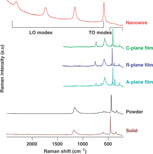
The enhanced TA modes below 300 cm–1 are also likely attributed to the enhancement with 488 nm pre-resonant excitation. We also observed a distinct intensity ratio of TA to LO modes in the solids and thin film, respectively. Since both solids and thin film consist of polycrystalline domains, the confined dimension in thin films appears to play a significant role in the overall polarity through the orientation of lattice packing. The broadening in LO modes is likely due to the excess Zn particles in the thin film which can reduce the ZnO bandgap Citation5. These LO modes, on the other hand, are much more significant in the thin film than in the solids. LO modes become the dominant peaks in the nanowires Raman spectra under 325 nm resonant excitation conditions, in which the multiple phonon modes are observed up to fourth order of the LO frequency, with negligible TA frequency. This can be explained with the strong electron–phonon interactions present in polar semiconductors, such as ZnO. LO modes appear to be more dominant in both nanowire and thin film than that in solids.
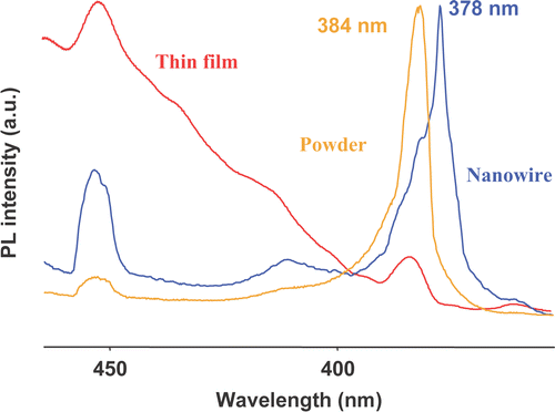
shows the photoluminescence emissions of the ZnO solids, thin film and nanowire respectively. The onset emission show the same thresholds in both cases; however, the nanowire shows discrete emission levels near the band edge while the solid and thin film samples have broad bound exciton emissions. This is indicative of possible bound-state and free exciton confinement in the nanowires. It is possibly due to stronger phonon and electron interactions in nanowires as it has not been observed in thin film and amorphous solids. This leads to an explanation to the trapped exciton level or as quantized exciton level due to the confinement in the cylindrical nanowire. It is also evident that the bandgap in the nanowire is blue shifted, consistent with the confinement exhibited by the nanometre size nanowires. The green emission in PL is believed to be due to the O2 deficiency.
Figure 2. Photoluminescence of ZnO in the solid, thin film and nanowire forms.
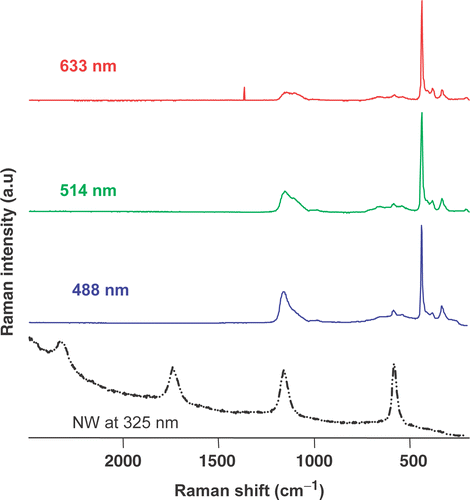
The resonant excitation can be further illustrated with bulk ZnO spectroscopy analyses depicted in the next two figures. shows ZnO powder vibration symmetry responses towards different laser excitation energies. The pre-resonant scattering at 488 nm excition is again confirmed. It is interesting to note that intensities of first and second order LO modes at 580 and 1152 cm–1 increase at this energy, which is lower than the bulk bandgap by more than 0.3 eV.
Figure 3. Raman spectra of ZnO powder excited with different laser wavelengths. The multiphonon ZnO nanowire resonant spectra are used for comparison.
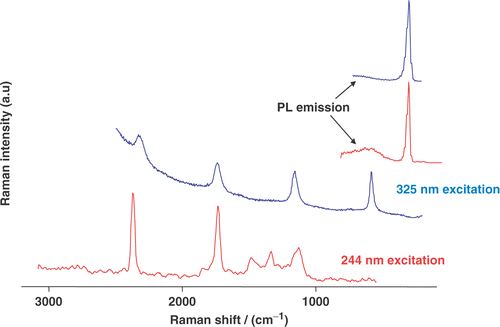
shows the ultraviolet Raman and photoluminescence spectra of solids and nanowires excited with 244 nm and 325 nm wavelength, respectively. The 244 nm excitation energy is much higher than the bandgap, while the 325 nm excitation is slightly below the bandgap. Therefore, photon fluxes from exciton emission near the band edge are much higher with 244 nm excitation than with 325 nm excitation. It is observed that the fourth and third orders of the electron–phonon interaction are even stronger than that under resonant excitation at 325 nm. We observed four major bands, centred at 577, 1152, 1734, and 2319 cm–1, with bandwidths at 30, 46, 55, and 53 cm–1, respectively. This result is consistent with the resonant excitations at 325 nm since different phonon vibration modes display different degrees of enhancement with the resonant excitations. This is depending on their contributions to the electronic polarizability via the electron–phonon interactions Citation6.
Figure 4. UV Raman and photoluminescence spectra of ZnO nanowires excited at 244 nm (red) and 325 nm (blue) respectively, showing the multiphonon vibration modes. The inset is the photoluminescence spectra.
4. Conclusion
We conclude that, with these Raman and photoluminescence spectroscopy observations, the electronic and optical properties of nanostructure ZnO materials can be significantly affected by the aspect ratio and the orientation of the domain ensemble. We observed a near-band-edge PL frequency shift with structure changes from a ZnO nanowire to its corresponding solid simultaneously. We are able to tune the ZnO bandgap, or electronic and optical properties, through the nanostructure geometry and polarity control, and through the density of states of surface phonons. Resonant Raman spectroscopy is a very sensitive technique to study nanowire electronic structures in relation to nanostructure analysis. The simultaneous Raman and photoluminescence investigations have the advantage of correlating the nanostructure with the electronic bandgap and the optical property changes of the semiconducting materials.
References
- Johnson , JC , Yan , H , Schaller , RD , Petersen , PB , Yang , P and Saykally , RJ . 2002 . Near-field imaging of nonlinear optical mixing in single zinc oxide nanowires . Nano Lett. , 2 : 317
- Gupta , R , Xiong , Q , Mahan , GD and Eklund , PC . 2003 . Surface optical phonon in gallium phosphide nanowires . Nano Lett. , 3 : 1745
- Yu , H , Li , J , Loomis , RA , Wang , L-W. and Buhro , WE . 2003 . Two- versus three-dimensional quantum confinement in indium phosphide wires and dots . Nat. Mater. , 2 : 517
- Ng , HT , Chen , B , Li , J , Han , J , Meyyappan , M , Wu , J , Li , SX and Haller , EE . 2003 . Optical properties of single-crystalline ZnO nanowires on m-sapphire . Appl. Phys. Lett. , 82 : 2023
- Exarhos , GJ , Rose , A and Windisch , C.F. Jr . 1997 . Thin Solid Films , 308–309 : 56
- Brunner , D , Angerer , H , Bustarret , E , Freudenberg , F , Höpler , R , Dimitrov , R , Ambacher , O and Stutzmann , M . 1997 . Optical constants of epitaxial AlGaN films and their temperature dependence . J. Appl. Phys. , 82 : 5090