Abstract
This paper deals with the fabrication of carbon nanotube field effect transistors (CNTFETs) for gas sensing applications. Such devices exploit the extremely sensitive change of the Schottky barrier heights between carbon nanotubes (CNTs) and drain/source metal electrodes: the gas adsorption creates an interfacial dipole that modifies the metal work function and so the band bending and the height of the Schottky barrier at the contacts. Our aim is to achieve the fingerprinting of a specific gas using a CNTFET based sensor array. This fingerprinting concept is based on the fact that the change of the metal electrode work function strictly depends on the metal/gas interaction. Consequently the CNTFET transfer characteristics will change specifically as a function of this interaction. To demonstrate this new concept, we have fabricated arrays of CNTFETs with different metal contacts: Au, Pd, Ti and Pt. Using these transistors, we have shown that a particular gas, in our case DiMethyl-Methyl-Phosphonate (DMMP, a sarin simulant), interacts specifically with each metal: 1 ppm of DMMP (15 min of exposure) reduces the transistor ON current by about 20% for Pt contacted CNTFETs and by nearly one order of magnitude for Pd contacted CNTFETs. We believe that this new approach can be applied for highly selective sensing of various gases, using ultra-compact, room temperature and very low power devices.
1. Introduction
The first paper showing the great potentiality of carbon nanotubes field effect transistors (CNTFETs) for gas sensing applications was published in 2000 Citation1. Since then, many teams have focused their interest on this new kind of sensor. These devices exploit the extremely sensitive change of the Schottky junctions built-up between carbon nanotubes (CNTs) and drain/source metal electrodes: the gas adsorption induces an interfacial dipole that changes the metal work function and so the bending and the height of the Schottky barrier at the contacts Citation2–4. It has been demonstrated that this kind of sensor can reach a sensitivity of 1 ppb for dimethyl-methyl–phosphonate (DMMP, a sarin simulant) Citation5. This sensitivity is highly sufficient for an effective Sarin gas detection: 17 ppb in 30 seconds is the joint service operational requirements (JSOR) for detectors Citation6 and 30 ppb up to 30 minutes is the immediate danger to health or life (IDHL) Citation6. The real issue is to improve the selectivity, thus reducing the risk of false alarm and various methods have been proposed so far. Among these methods, the deposition of polymers on the CNTFETs (functionalisation) is extensively studied and very promising results have been already obtained (see e.g. Citation7). However, the use of polymers could present several drawbacks such as increasing the sensor response time and decreasing its lifetime, as methods currently used to desorb analyte molecules (thermal anneal and UV exposition) should degrade these polymers. Another issue is the lack of knowledge on the real physical effect of polymers: up to now the choice of a particular polymer continues to be empirical and this also holds for biosensing applications Citation8.
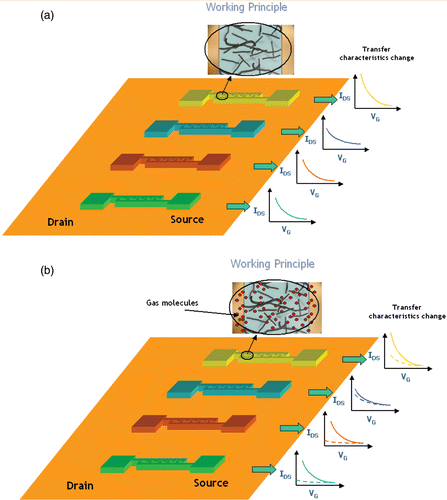
Our approach for solving this selectivity problem, is to fabricate a sensor comprising an array of n CNT-based transistors. Each transistor will use a different metal as source/drain electrodes. Using different metals implies that in each CNTFET, the contact situation will be different. As a consequence the Fermi level alignment between the various metals and the CNTs will change and therefore the characteristics of the Schottky barrier at the junction will, change as well. We want to demonstrate that, after being exposed to a specific gas, the n transistors, taken altogether, will react in a unique way, thus yielding a specific signature of this gas. This principle is illustrated on for the case of 4 transistors (n = 4).
Figure 1. (a) Four CNTFETs fabricated with four different metal interdigited electrodes (each colour corresponds to a different metal): in the inset, the carbon nanotubes chains connecting the two electrodes. On the right hand side, the transfer characteristic (source/drain current as a function of the gate voltage) of each transistor in air. (b) Change of the transfer characteristic of the four transistors as a consequence of the exposition to a particular gas (in the inset, the gas molecules that interact with the transistor): the four transfer characteristics change in a different way as a consequence of the various metal contacts (dashed line). Each gas gives a unique ‘signature’ in terms of IDS variation over the four transistors.
Another advantage of using this technique of gas fingerprinting, is that gas molecules desorption can be easily achieved using either UV light exposure Citation9 or thermal heating Citation10 without risking to degrade the device performances. Finally, the sensing mechanism (change of metal work function) is well understood Citation11–13 and this will ease the device parameter optimisation.
2. Theory
As mentioned in the introduction, the first paper dealing with the use of CNTFETs for gas sensing applications was published in 2000 by Stanford University Citation1. In this paper, the same CNT-based transistor was exposed to NO2, NH3 and ambient air. The transfer characteristic (IDS-VG) showed a shift of the ‘turn-on’ voltage after being exposed to different gases. Initially this effect was attributed to doping of the carbon nanotube by charge transfer. In 2003, the Avouris team (IBM) observed that oxygen adsorption also led to a shift of the turn-on voltage but demonstrated that this effect resulted from the modification of the metal-nanotube junction rather than from a doping effect Citation12. Therefore the change of the junction characteristics after exposure to a gas is related to the modulation of the contact resistance and not of the channel conductance Citation14. Recently, these results have been confirmed by other teams Citation15 as well as by Stanford University in 2004 Citation8. Bauschlicher et al. (NASA Aimes Research Center) Citation16 theoretically confirmed that NH3 molecules have only a weak interaction with carbon nanotubes and graphite: their binding energy is very low and there is little charge transfer with no change in the nanotube band gap Fermi level (plutot que band gap). This last conclusion confirms that gas species do not dope the carbon nanotubes. From a theoretical point of view, the effect of a gas specie on the metal/CNT junction can be explained by using the model developed for organic compounds-to-metal junctions Citation13, Citation17. Actually in this case the interface is characterised by the presence of dipoles which generate an electrostatic potential close to the electrodes. The presence of the interface dipoles created at the contact modifies the energy of the electronic levels in organic compounds and the work function of the metal surface. When the interface dipole points its negative pole towards the organic film and its positive pole towards the metal, the result is an increase of both the metal work function and the highest occupied molecular orbital (HOMO) energy of the organic film, by addition of an electrostatic energy. Therefore, the hole injection barrier is reduced. On the other hand, when the dipole direction is reversed, the metal work function is reduced and so is the electron injection barrier. In the case of a metal/CNT junction, similarly, the gas molecules introduce electric dipoles at the interfaces and modify the intensity of the dipole settled at the metal/CNT junction.
This change influences directly the metal work function and the Fermi level alignments. This consideration agrees with the simulations and experimental results in the case of oxygen exposure obtained by IBM Citation18: changing the oxygen concentration changes the dipole strength and the metal work function is increased, thus reducing the hole injection barrier (the hole current raises). The same interpretation can be made when the metal/CNT Schottky barrier is modulated using polar chemical compounds Citation19. From a sensing point of view, we can observe that a gas (or different gases) can change the transfer characteristics of the CNT-based transistor Citation1. We propose to use this mechanism to obtain the fingerprinting of a particular gas using n different metals for the contacts: analyzing the variation of the transfer characteristics of all n transistors after gas exposure could identify a gas specie unambiguously.
Starting from these considerations, our approach is to fabricate an array composed by several CNT-based transistors. Each transistor will be manufactured using different metals as source/drain electrodes. In our case we have decided to use four different metals for the electrodes: Au, Pd, Pt and Ti. The work functions for these metals are respectively 5.1 eV for the Au and Pd, 5.65 eV and 4.33 eV, respectively for Pt and Ti Citation20–23. This choice was justified by the purpose of verifying if the gas interaction is related only to the work function difference between the different metals or if it depends on the specific nature of the gas and of the electrode. If the interaction is only related to the work function difference, the change of the CNTFET based sensors response (transfer characteristic) will be nearly the same for Au and Pd when they are exposed to the same gas after having been exposed to the same gas. If the gas interacts differently with the two metals and so with the junctions, the transfer characteristic change will be not the same.
3. Sample preparation
Our samples have been fabricated using n-doped silicon substrates (that serve as a gate electrode) covered with 50 nm of thermally grown SiO2. The electrodes have been obtained by standard evaporation and liff-off techniques. The metal thickness was typically 35 nm. A 5 nm thick Ti layer was first evaporated in order to improve the adhesion of the Au, Pd, Pt layers on the substrate. The geometrical configuration of the metal electrodes has been optimised using interdigited metal fingers: in this way the possibility to obtain a connecting chain of carbon nanotubes (from random networks) is maximised. Finger distance varies between 2 and 1 µm. The following step is to deposit the carbon nanotubes random network between the metal electrodes. This deposition starts by the fabrication of a suspension of carbon nanotubes in a liquid medium, in our case dimethylformamide (DMF). One of the most important issues to overwhelm is constituted by the fact that carbon nanotubes are naturally grouped in bundles by Van der Waal forces. First, CNT bundles and residual impurities (e.g., catalyst particles) have to be eliminated from the original CNT suspension. This can be accomplished by sonication to ‘break’ the bundles, followed by centrifugation (two phases of 10 minutes at 3000 rpm) and careful recuperation of the supernatant part of the suspension. We optimised our process changing the sonication time (1, 2, 3, 4, …, 7 hours). Subsequently, the solution is deposited between the finger electrodes using a micropipette and analysed using SEM or AFM facilities.
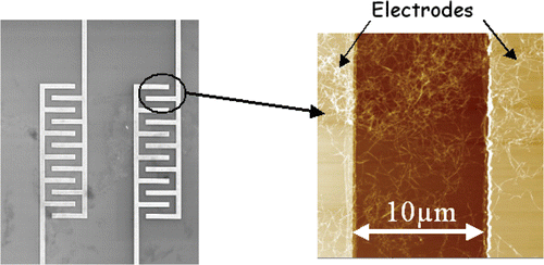
Finally, we observed that for sonication times longer than 3 hours we did not observe a significant improvement of dispersion uniformity. Actually, as we can see in the SEM picture in , three hours of sonication yield a quite good uniform mat (according to our final application). Another important issue is that CNTs always come in mixtures of semiconductor and metallic specimens. No method, up to now, exists for separating semiconductor from metallic specimens in an easy and rapid way. However, as far as random networks are concerned, it has been demonstrated that, through a percolation effect, overall semiconductor behaviour could be obtained, for carefully controlled surface densities Citation24. Only two conditions must be fulfilled: the distance between the two electrodes must be larger than the carbon nanotubes length (otherwise metallic nanotubes could cause a short-circuit) Citation25, Citation26 and the areal density of the deposited SWNTs has to be controlled carefully, because above the percolation threshold, for high surface densities (5 to 10 µm2), the conduction is practically ohmic with no gating effect Citation24–26. The carbon nanotubes used for this work are super purified nanotubes. Their impurity content is less than 5%, their diameter and length are respectively, before sonification, 1.0 nm ± 0.2 nm and 100–1000 nm. Typical transistors manufactured using suspensions of CNTs in DMF are shown in . As we can see in , on the right-hand side, the CNT distribution is quite uniform and CNTs clearly link the source and drain electrodes. Remember that the gate electrode (doped Si substrate) is underneath the CNT mat.
Figure 2. SEM picture of a CNT mat dispersed on a substrate after having been sonicated for three hours and centrifuged at 3000 rpm (2 times 10 minutes).
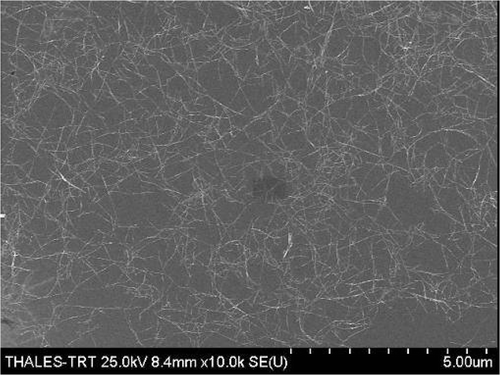
Figure 3. Left-hand side: SEM image of interdigited CNT transistors, Right-hand side: AFM detail of carbon nanotubes random network between two electrodes.
4. Test
We started the test phase performing measurements of the electrical behaviour of the different junctions. In our case the most important characteristic is the evolution of the current between drain and source as a function of the gate voltage. Around 50% of the transistors are effective. Most of them are characterised by a distance between the interdigited electrodes of more than 5 µm. Actually, those with a distance between the electrodes less than 5 µm, show a metallic behaviour: the distance is too low and some chains connecting the two electrodes are composed only by metallic CNTs. After the initial measurements in air, we have exposed the transistors to a DMMP gas concentration of 1 ppm during 15 minutes and we have measured the change of the transfer characteristics keeping constant the value for the source/drain bias (VDS = 1V).
As we can see in , IDS change is very different for the CNTFETs fabricated using different metals. At a gate voltage VG of about −25 V, the Pd, Au, Ti and Pt drain currents are reduced respectively to 10%, 35%, 50% and 80% of their initial values measured in air. For larger VG values, the transistors reach the saturation threshold or the oxide breakdown voltage.
Figure 4. (a)–(d). Transfer characteristics change for the different metal electrodes after exposure to 1ppm of DMMP (VDS = 1V).
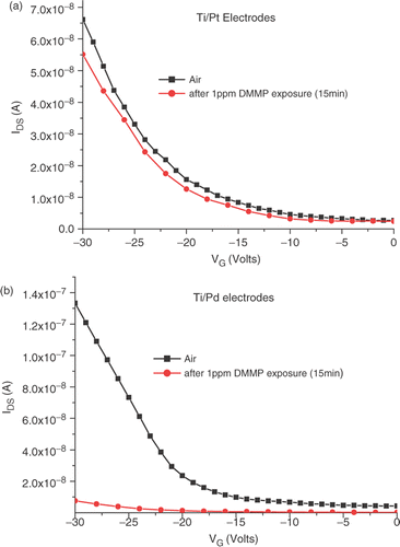
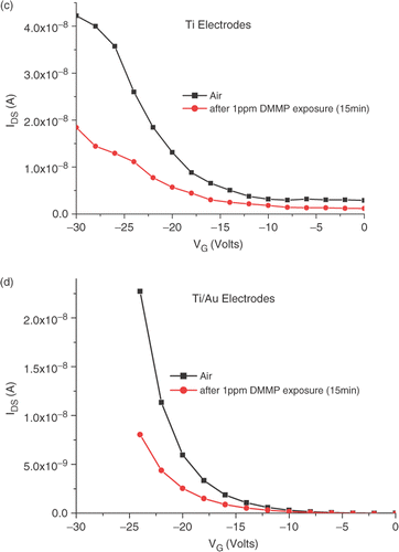
We have performed several measurements using different electrodes design (20 transistors for each metal with different metal finger distance) and these results are quite reproducible: it seems that the sensor sensitivity is not influenced by the number of nanotubes linking the electrodes. Indeed, the result dispersion for each metal is around ± 5%, which is reasonable considering the difference in current reduction percentage. From these measurements, we can assert that different metals interact in a different way with the DMMP. Particularly interesting is the fact that the Pd and Au transfer characteristic change is very different even if the metal work functions are nearly the same. This indicates that the change in the CNTFETs characteristics is not simply related to the metal work function difference but very probably to a specific chemical interaction between the metal and the gas: the DMMP influences the change of each metal work function in a very specific way and so the change of the electric response of the transistor.
5. Conclusions and Perspectives
In this work, we have demonstrated that CNTFET based array could, potentially, be used to obtain an electronic fingerprinting of specific gases. We have demonstrated that the DMMP interacts differently with each metal electrode by changing the metal work function and so the transfer characteristics of the CNTFET. This effect does not depend on the initial metal work function but on a specific chemical interaction between the metal and the gas. Measurements using different gases must be performed in order to confirm the validity of our concept.
References
- Kong , J , Franklin , NR , Zhou , C , Chapline , MG , Peng , S , Cho , K and Dai , H . 2000 . Nanotube molecular wires as chemical sensors . Science , 287 : 622 – 625 .
- Martel , R , Derycke , V , Lavoie , C , Appenzeller , J , Chan , KK , Tersoff , J and Avouris , Ph . 2001 . Ambipolar electrical transport in semiconducting single-wall carbon nanotubes . Phys. Rev. Lett. , 87 : 256805
- Collins , PG , Bradley , K , Masa , Ishigami and Zettl , A . 2000 . Extreme oxygen sensitivity of electronic properties of carbon nanotubes . Science , 287 : 1801 – 1804 .
- Derycke , V , Martel , R , Appenzeller , J and Avouris , Ph . 2002 . Controlling doping and carrier injection in carbon nanotube transistors . App. Phys. Lett. , 80 : 2773 – 2775 .
- Novak , J , Snow , E , Houser , E , D.P. , McGill , JL and Stepnowski , R . 2003 . Nerve agent detection using networks of single-walled carbon nanotubes . App. Phys. Lett. , 83 : 4026 – 4028 .
- Hulet , SW , Sommerville , DR , Benton , BJ , Forster , JS , Scotto , JA , Muse , W , Crosier , RB , Reutter , SA , Mioduszewski , RJ and Thomson , SA . 2007 . “ Edgewood Chemical Biological Center, U.S. Army Research, Development and Engineering Command ” . In Low-level cyclo-sarin (GF) vapor exposure in the Gottingen minipig: effect of exposure concentration and duration on pupil size , Abingdon, MD , , USA : Tech Rep. ADA469336 . Available at http://www.dtic.mil/srch/doc?collection=t2&id=ADA469336
- Qi , P , Vermesh , O , Grecu , M , Javey , A , Wang , Q , Dai , H , Peng , S and Cho , KJ . 2003 . Toward large arrays of multiplex functionalized carbon nanotube sensors for highly sensitive and selective molecular detection . Nano Lett. , 3 : 347 – 351 .
- Chen , R , Choi , H , Bangsaruntip , S , Yenilmez , E , Tang , X , Wang , Q , Chang , Y-L and Dai , H . 2004 . An investigation of the mechanisms of electronic sensing of protein adorption on carbon nanotube devices . J. Am. Chem. Soc. , 126 : 1563 – 1568 .
- Chen , R , Franklin , N , Kong , J , Cao , J , Tombler , T , Zhang , Y and Dai , H . 2001 . Molecular photodesorption from single-walled carbon nanotubes . Appl. Phys. Lett. , 79 : 2258 – 2001 .
- Li , J , Lu , Y , Ye , Q , Delzeit , L and Meyyappan , M . 2005 . A gas sensor array using carbon nanotubes and microfabrication technology . Electrochem. Solid-State Lett. , 8 : H100 – H102 .
- Appenzeller , J , Knoch , J , Martel , R , Derycke , V , Wind , S and Avouris , Ph . 2002 . Carbon nanotube electronics . IEEE Trans. Nanotech. , 1 : 184 – 189 .
- Avouris , Ph , Appenzeller , J , Martel , R and Wind , SJ . 2003 . Carbon nanotube electronics . Proc. IEEE , 91 : 1772 – 1784 .
- Crispin , X , Geskin , VM , Crispin , A , Cornil , J , Lazzaroni , R , Salaneck , WR and Brédas , JL . 2002 . Characterization of the interface dipole at organic/ metal interfaces . JACS , 124 : 8131 – 8141 .
- Appenzeller , J , Knoch , J , Radosavljevic , M and Avouris , Ph . 2004 . Tunneling versus thermionic emission in one-dimensional semiconductors . Phys.Rev.Lett. , 92 : 048301
- Zhang , J , Boyd , A , Tselev , A , Paranjape , M and Barbara , P . 2006 . Mechanism of NO2 detection in carbon nanotube field effect transistor chemical sensors . App. Phys. Lett. , 88 : 123112
- Bauschlicher , CW Jr and Ricca , A . 2004 . Binding of NH3 to graphite and to a (9,0) carbon nanotube . Phys Rev. B , 70 : 115409
- Crispin , X . 2004 . Interface dipole at organic/metal interfaces and organic solar cells, Sol. Energy Mat. Sol. Cells , 83 : 147 – 168 .
- Heinze , S , Tersoff , J , Martel , R , Derycke , V , Appenzeller , J and Avouris , Ph . 2002 . Carbon nanotubes as Schottky barrier transistors . Phys. Rev. Lett. , 89 : 106801
- Auvray , S , Borghetti , J , Goffman , M , Filoramo , A , Derycke , V , Bourgoin , J and Jost , O . 2004 . Carbon nanotube transistor optimization by chemical control of the nanotube-metal interface . App. Phys. Lett. , 84 : 5106 – 5108 .
- Morikawa , Y , Ishii , H and Seki , K . 2004 . Theoretical study of n-alkane adsorption on metal surfaces . Phys. Rev. B , 69 : 041403
- Mori , T , Kozawa , T , Ohwaki , T , Taga , Y , Nagai , S , Yamasaki , S , Asami , S , Shibata , N and Koike , M . 1996 . Schottky barriers and contact resistances on p-type GaN . Appl. Phys. Lett. , 69 : 3537 – 3569 .
- Periodic Table of Elements. Available at: http://environmentalchemistry.com/yogi/periodic/Au.html; http://environmentalchemistry.com/yogi/periodic/Ti.html; http://environmentalchemistry.com/yogi/periodic/Pd.html
- Yang , MH , Teo , KBK , Milne , WI and Hasko , DG . 2005 . Carbon nanotube Schottky diode and directionally dependent field-effect transistor using asymmetrical contacts . Appl. Phys Lett. , 87 : 253116
- Snow , E , Novak , J , Lay , M , Houser , E , Perkins , F and Campbell , P . 2004 . Carbon nanotube networks: nanomaterial for macroelectronic applications . J. Vac. Sci. & Technol. B , 22 : 1990 – 1994 .
- Kumar , S , Murthy , JY and Alam , MA . 2005 . Percolating conduction in finite nanotube networks . Phys. Rev. Lett. , 95 : 066802
- Kumar , S , Pimparkar , N and Murthy , JY . 2006 . Theory of transfer characteristics of nanotube network transistors . App. Phys. Lett. , 88 : 123505