Abstract
Heterojunction photovoltaic devices were fabricated using single crystal silicon nanowires and the organic semiconductor regioregular poly-(3-hexyl thiophene) (RR-P3HT). N-type nanowires were first grown on an n+ silicon substrate by the vapor-liquid-solid (VLS) method. Devices were then fabricated by filling the gap between the nanowires and a transparent indium tin oxide (ITO) glass electrode with a polymer. For initial devices the gap was filled with P3HT deposited from chlorobenzene solution. Device performance indicates that both silicon and P3HT act as absorbers for photovoltaic response, but that photocurrents were very low due to high series resistance in the cell. A second type of device was fabricated by depositing a thin layer of P3HT on the grown nanowires by dip coating from a dilute solution, and then filling the voids between nanowires and the transparent electrode with the conductive polymer poly-[3,4-(ethylenedioxy)-thiophene]: poly-(styrene sulfonate) (PEDOT:PSS). The relatively high mobility of this organic conductor results in much higher photocurrents in photovoltaic cells, but results in a dip in the spectral response of the cells in the blue-green region due to light absorption in the conducting polymer. These materials show promise for efficient low-cost photovoltaic devices, but the cell geometry and materials interfaces will need to be optimized to reach their potential.
1. Introduction
Polymeric organic semiconductors have been used to fabricate photovoltaic materials for more than a decade with steady improvement in both materials and device architectures Citation1. Some of the advantages of these materials are ease of fabrication and high optical absorption by thin films. However, charge carrier mobilities are typically orders of magnitude lower than commonly used inorganic semiconductors. In addition, excitons in organic semiconductors have a much high binding energy than crystalline inorganic semiconductors, and thus relatively large electric fields are required for dissociation into charge carriers after photoexcitation. The fields necessary for exciton dissociation (and hence charge carrier formation) exist only at heterointerfaces, and thus organic layers must be kept relatively thin to produce efficient devices.
In order to exploit some of the advantages of organic semiconductors while minimizing the impact of their major disadvantage, poor charge transport, photovoltaic devices have been fabricated using bulk heterojunctions of organic polymers with silicon nanowires. In this configuration there are interpenetrating networks of materials, minimizing the distance that excitons must travel before dissociating at a heterointerface. A particularly successful version of this type of device uses (6,6)-phenyl C61 butyric acid methyl ester (PCBM) as the donor, resulting in efficiencies exceeding 3% Citation2. A natural extension of this idea is the use of inorganic semiconductors as one of the materials. Effective photovoltaic devices have been fabricated using inorganic nanoparticles or nanorods Citation3. The problem that occurs with this type of architecture is that one of the conduction paths requires percolation of charges to reach the contact electrode. In this work we propose the use of doped single crystal nanowires as the inorganic material in an organic-inorganic bulk heterojunction photovoltaic cell. The n-type silicon nanowires are grown on a highly doped n-type silicon substrate, resulting in a continuous conducting pathway for charge carriers in the inorganic phase.
A nanowire geometry has been proposed for silicon photovoltaic devices to improve device performance Citation4. This geometry improves charge collection while maintaining light absorption when the mean free path for charge carriers is short. Silicon nanowires are typically grown using Au particles as a catalyst for VLS growth. The presence of small amounts of gold in the nanowires will reduce carrier lifetimes since gold acts as a deep trap in silicon. Carrier lifetime should be greater than 1 ns, however, due to the low solubility of gold in silicon Citation5. Charge collection from a nanowire geometry via a conductive polymer adds two possible complications: charge transport across the silicon-polymer interface must be favorable, and carrier tranport in the polymer (holes for the device type investigated here) must be efficient. The devices fabricated in this investigation are designed to answer some of these questions.
2. Nanowire fabrication
Silicon nanowires were fabricated via a VLS growth mechanism on n-type silicon (111) wafers. The wafers were coated with a thin Au film (∼2 nm) by sputtering or evaporation, then placed in tube furnace on a Mo block for nanowire growth. Nanowires were grown at 420–450°C using 10% disilane in Ar at a pressure of 2 Torr. Full details of the growth have been previously published Citation6. N-type doping of the nanowires was achieved by incorporating 100 ppm phosphine into the gas flow used during growth, producing a doping level of approximately 3 × 1016 cm−3 as determined by secondary ion mass spectroscopy Citation7.
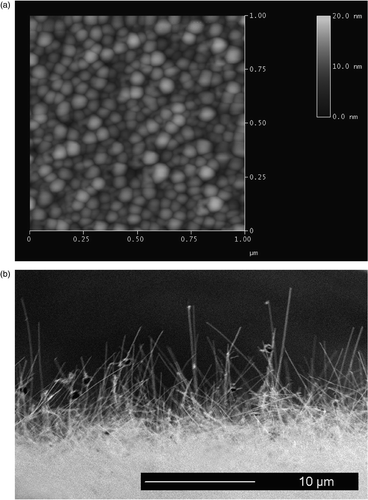
Growth of nanowires via the VLS process occurs at reaction sites comprised of small Au islands. To determine the size and density of Au islands produced on the substrates used in these experiments, a 1–2 nm thick Au film was deposited on a Si wafer, the wafer was heated to the growth temperature used for nanowire growth in the tube furnace, then cooled and examined using atomic force microscopy (AFM). shows an AFM scan taken with a Digital Instruments microscope of an Au film after annealing at 420°C. Au nanoparticle diameters were 46 ± 17 nm, and particle density on the surface was 3.7 × 10¹⁰ particles/cm2. Silicon nanowire diameters are typically several nm larger than the size of the Au nanoparticles used to nucleate and control the growth in the VLS process Citation8. The length of the nanowires used in these experiments was 15–20 µm, produced during a 15 min. growth period in the tube furnace. The length varies between individual wires, with some dependence on wire diameter.
Figure 1. (a) AFM image (tapping mode) of Au nanoparticles on a silicon surface following anneal at 420°C. (b) SEM cross-section showing the nanowires resulting from a 15 min. growth on a similar Au nanoparticle film.
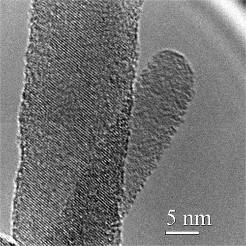
The silicon nanowires used in these experiments were single crystalline material with a principle growth axis along the (111) direction, as shown in the HRTEM image in . The wire tips are typically terminated with Au, and the edges of the wires have an amorphous SiO2 layer approximately 0.4 nm thick. To provide better junctions between the n-type nanowires and the p-type organic semiconductor used to create the p-n heterojunction, the oxide was etched in buffered HF immediately prior to placing the nanowire samples in a nitrogen glove box for device fabrication.
Figure 2. HRTEM image of silicon nanowire showing crystalline core and thin amorphous oxide at the edges of the wire.
Quantum effects are important in small silicon nanowires, increasing the bandgap and causing the lowest energy transition to be direct. However, both theory and experiment have shown that these effects are only important for wire diameters below approximately 8 nm Citation9, Citation10. Thus the wires used in these experiments, with an average diameter of nearly 50 nm, behave essentially like bulk silicon as far as electronic transitions are concerned. However, the area of the heterojunction is considerably larger than would be the case for planar devices without nanowires. For the wire parameters discussed above, the area increase is approximately 2 × 10⁴ greater than for a planar device. The random orientation of wires has the additional benefit of trapping more light than would a planar or textured surface.
3. Organic–inorganic devices
For this work, we chose to use regioregular poly(3-hexylthiophene) as the p-type organic semiconductor at the heterointerface due to its high carrier mobility and low bandgap (2.0 eV) compared to other polymeric semiconductors. The interface between silicon and organic semiconductors has been investigated by a number of groups Citation11–13. The heterojunction between n-Si and RR-P3HT was found to be a nearly ideal diode with a rectification ratio of greater than 103 Citation12. Due to the fact that the nanowires used in this study were grown on an opaque n-Si wafer, the contact to the P3HT was made using a transparent ITO conductor on glass. Poly-[3,4-(ethylenedioxy)-thiophene]: poly-(styrene sulfonate) (PEDOT:PSS) has been widely used as a hole transport layer Citation1, and was used in our devices between the P3HT organic semiconductor and ITO electrode.
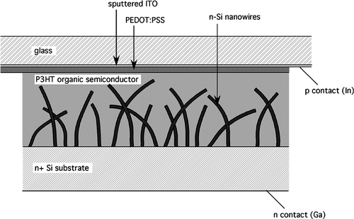
The structure of the devices fabricated for this study is shown in . Nanowires were first grown on an n-type silicon substrate, and transferred to a nitrogen glove box following a brief (10 sec.) HF etch to remove surface oxide. PEDOT:PSS (Bayer Baytron P) was spin coated onto glass with a thin transparent electrode of sputtered ITO and also transferred to the glove box after annealing in air for 1 hr at 150°C. Several drops of a solution of P3HT in chlorobenzene (5 g/l, deoxygenated by nitrogen bubbling) were applied to the surface of the PEDOT-PSS film, and the n-Si nanowire sample was placed face-down on top of the transparent electrode. The P3HT film was allowed to evaporate slowly over several days, then the sandwich was annealed for 1 hr at 100° C to allow the P3HT film to form an oriented layer Citation14. The device was then sealed with epoxy and removed from the glovebox for testing. Contact to the n side of the cell was made by scratching the back surface of the n-Si wafer to remove oxide and applying a Ga contact; contact to the p side was made by soldering a wire to the ITO using In-alloy solder. The active area of the cell was approximately 3.2 cm2.
Figure 3. Diagram of the silicon nanowire PV cell structure (not to scale).
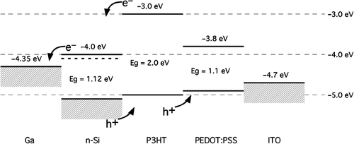
Energy levels relative to the vacuum level are shown in for the components of the photovoltaic cell (without any adjustments for dipole formation or band bending due to Fermi levels). The HOMO of P3HT is positioned to inject holes into PEDOT-PSS and hence into the ITO electrode, and should accept holes generated by light absorption in the silicon nanowires. The LUMO of P3HT is well above the Fermi level of the n-Si nanowires and electron collection should occur efficiently at the silicon interface. Electrons generated in the nanowires will be collected at the Ga electrode.
Figure 4. Energy levels of components of the cell.
Diode characteristics were observed for the assembled devices (). However, a relatively high leakage current was observed in the reverse direction. A likely suspect for this is nanowire penetration of the P3HT and possibly PEDOT:PSS layers during drying of the P3HT layer due to hydrostatic forces. Another possibility for high currents through the device is degradation of the P3HT polymer through exposure to oxygen. Although materials were handled in a nitrogen glove box and encapsulated prior to testing, this failure mechanism is well known for P3HT devices Citation15. There may also be carrier recombination at the heterointerface, although P3HT heterojunction devices have been fabricated with very high internal quantum efficiency and low recombination Citation16.
Figure 5. IV curve for a silicon nanowire-P3HT PV cell under 100 mW/cm2 illumination (×) and dark (+). Inset shows short-circuit photocurrent as a function of wavelength.
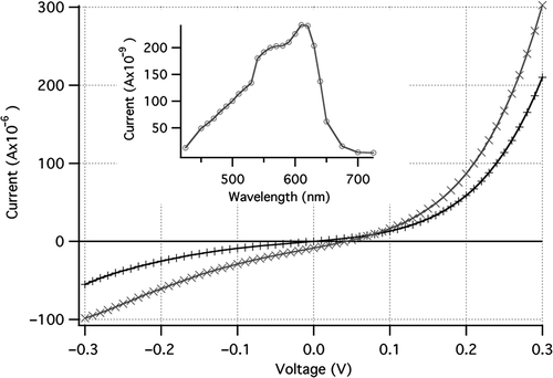
The peak in photoresponse of the cell is near 600 nm ( inset). The absorption peak of P3HT is between 500 and 550 nm (2.0 eV bandgap), and a smaller peak in short-circuit photocurrent is observed in this wavelength region. Since the main photocurrent peak is to the red of this, however, a substantial fraction of the photovoltaic response must be due to absorption in the silicon nanowires. The open circuit voltage for the initial set of devices (0.05 V) was much lower than expected, due most likely to a low shunt resistance in the cells. High dark currents in the devices are likely due to the large surface area of the p-n junction, and indicate that conduction barriers between the silicon and polymer are not present. Oxidation of the Si nanowire surface would limit currents to lower values than those observed.
Low short circuit photocurrents in the devices fabricated (Jsc = 2.6 × 10⁻⁶ A/cm2 at 100 mW/cm2 illumination) are likely due to the assembly method chosen, which requires a much thicker layer of P3HT than would be optimal. Carrier mobilities are rather low in P3HT, and holes generated in the silicon nanowires must be transported across the P3HT film to the ITO electrode. For light absorbed in the P3HT layer, excitons are generated which must diffuse to a heterojunction for dissociation and collection. The P3HT layer thickness should thus be kept very thin to permit exciton diffusion and carrier collection. Hence, an alternate geometry was investigated to improve device efficiency.
A second type of photovoltaic cell was fabricated using exactly the same material system as the first, but applying the P3HT as a thin film. The n-doped silicon nanowires on a silicon substrate were dipped into a solution of P3HT in chlorobenzene (5 g/l) and allowed to dry in a vertical position under nitrogen. The film thickness of the P3HT layer was estimated by ellipsometric measurements of a similar film on a planar silicon substrate as 50 nm. The P3HT film was allowed to dry in a nitrogen atmosphere for several days, then a PV cell was assembled by dropping PEDOT:PSS (Aldrich, de-oxygenated by bubbling nitrogen for 1 hr) onto the nanowires and then sandwiching them under an ITO glass electrode as before. The cells were annealed in nitrogen at 125°C, and then encapsulated with epoxy for testing. Initial devices showed nearly linear IV characteristics which was thought to be due to shorting of the nanowires to the ITO electrode. Mixing a small amount of 20–50 µm glass microballoons with the PEDOT:PSS prior to assembling the cell produced devices with diode-like IV characteristics.
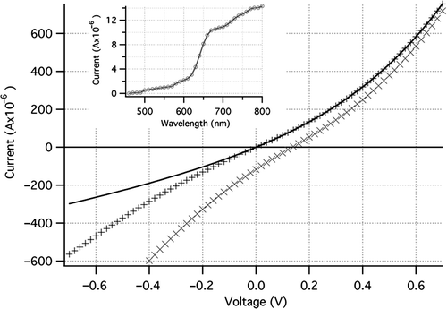
A relatively high leakage current was observed in the reverse direction of the IV curve for the photovoltaic cell (). This is again due to the large area of the p-n junction, this time with more efficient carrier transport through the conducting polymer to the ITO electrode. The open circuit voltage of the cell is still low (0.15 V), but short circuit photocurrent has increased more than an order of magnitude over the cell with a thick P3HT layer. The photoresponse action spectrum ( inset) is much different from that seen in the first type of cell: little photocurrent is observed below 600 nm. This is explained by the thick layer of PEDOT:PSS (∼50 µm) which has some absorption in the visible (bandgap = 2.0 eV) but does not contribute to photocurrent in the cell. Thus nearly the entire photoresponse of the cell is due to absorption in the silicon since little light more energetic than 2 eV reaches the P3HT layer. Large improvements photoresponse can be expected for cells where silicon nanowire growth is optimized to produce nanowires of all the same height, and thus parasitic absorption in a thick contact polymer layer is eliminated.
Figure 6. IV curve for a silicon nanowire-P3HT PV cell with a thin P3HT layer under 100 mW/cm2 illumination (×) and dark (+). Fit of forward dark current to the current equation below is shown as a solid line. Inset shows the short-circuit photocurrent as a function of wavelength.
The low open circuit voltages observed in these cells is likely due to shunt currents in the devices (high dark current). In order to analyze the impact of shunt current, the photovoltaic cells were modeled as a diode in parallel with a current source, together with parasitic series and shunt resistors. The resulting equation for current in the cell is
Table 1. Photovoltaic cell parameters for two types of devices fabricated.
Open circuit voltage can be found by setting the current to zero in the above equation:
The open circuit voltage depends on the logarithm of the photo-generated current (light intensity), and also depends strongly on shunt resistance in the cell–as shunt resistance decreases, Voc also decreases. For the type of cell fabricated here (n-type semiconductor and p-type semiconducting polymer), the maximum open circuit voltage should be the ionization potential of the donor (RR-P3HT, IP∼5.0 eV) minus the electron affinity of the acceptor (silicon, EA∼4.0 eV) minus the exciton binding energy (∼0.3 eV) Citation19. The open circuit voltage is reduced for low illumination levels, high values for J 0, and low values of Rsh . It is thus important to minimize dark current (current leakage paths and recombination) to achieve good conversion efficiency in photovoltaic cells. Recombination likely occurs at traps near the heterojunction interface, and is thus dependent on interfacial area in the cell. The cell interface area in this case is controlled by wire diameter, and there will be an optimum value that balances improvement in charge collection against degradation of open circuit voltage and short circuit current.
4. Conclusions
Photovoltaic cells using heterojunctions of n-type silicon nanowires and P3HT organic semiconductor have been assembled and analyzed. The cells show evidence of carrier generation in both the silicon and polymer sides of the heterojunction. Initial devices had a relatively thick layer of P3HT resulting in high series resistance and very low efficiency. Subsequent devices using a thin layer of P3HT and a thicker layer of PEDOT:PSS polymer as the contact layer had much lower series resistance but had high parasitic light absorption in the contact polymer. The nanowire geometry shows promise for both high light absorption and efficient carrier transport to electrodes, but device geometry and materials characteristics need to be optimized. Efforts are underway to modify materials parameters (nanowire doping, polymer thickness, and charge transport layer composition) to improve device characteristics.
Related Research Data
References
- Hoppe , H and Sariciftci , NS . 2004 . Organic solar cells . J. Mater. Res. , 19 : 1924 – 1945 .
- Padinger , F , Rittberger , RS and Sariciftci , NS . 2003 . Effects of postproduction treatment on plastic solar cells . Adv. Funct. Mater. , 13 : 85 – 88 .
- Huynh , WU , Dittmer , JJ and Alivisatos , AP . 2002 . Hybrid nanorod-polymer solar cells . Science , 295 : 2425 – 2427 .
- Kayes , BM , Atwater , HA and Lewis , NS . 2005 . Comparison of the device physics principles of planar and radial p-n junction nanorod solar cells . J. Appl. Phys. , 97 : 114302-1 – 114302-11 .
- Sze , SM . 1981 . Physics of semiconductor devices , 2nd , New York : John Wiley & Sons .
- Decker , CA . 2004 . Directed growth of nickel silicide nanowires . Appl. Phys. Lett. , 84 : 1389 – 1391 .
- Goncher , G . 2006 . P-N junctions in silicon nanowires . J. Electronic Materials , 35 : 1509 – 1512 .
- Cui , Y . 2001 . Diameter-controlled synthesis of single-crystal silicon nanowires . Appl. Phys. Lett. , 78 : 2214 – 2216 .
- Delley , B and Steigmeier , EF . 1995 . Size dependence of band gaps in silicon nanostructures . Appl. Phys. Lett. , 67 : 2370 – 2372 .
- Ma , DDD . 2003 . Small-diameter silicon nanowire surfaces . Science , 299 : 1874 – 1877 .
- Williams , EL . 2005 . Conducting polymer and hydrogenated amorphous silicon hybrid solar cells . Appl. Phys. Lett. , 87 : 223504-1 – 223504-3 .
- Chen , CH and Shih , I . 2006 . Hybrid organic on inorganic semiconductor heterojunction . J. Mater. Sci.: Mater. Electron. , 17 : 1047 – 1053 .
- Gowrishankar , V . May 2006 . “ Amorphous-silicon/polymer solar cells and key design rules for hybrid solar cells ” . In Paper presented at the IEEE 4th World Conference on Photovoltaic Energy Conversion May , 5 – 12 . Hawaii
- Li , G . 2005 . Investigation of annealing effects and film thickness dependence of polymer solar cells based on poly(3-hexylthiophene) . J. Appl. Phys. , 98 : 043704-1 – 043704-5 .
- Gelinck , GH , Geuns , TCT and de Leeuw , DM . 2000 . High-performance all-polymer integrated circuits . Appl. Phys. Lett. , 77 : 1487 – 1489 .
- Schilinsky , P , Waldauf , C and Brabec , CJ . 2002 . Recombination and loss analysis in polythiophene based bulk heterojunction photodetectors . Appl. Phys. Lett. , 81 : 3885
- Xue , J . 2004 . 4.2% efficient organic photovoltaic cells with low series resistances . Appl. Phys. Lett. , 84 : 3013
- Schroder , DK . 1998 . Semiconductor material and device characterization , 2nd , New York : John Wiley and Sons .
- Rand , BP , Burk , DP and Forrest , SR . 2007 . Offset energies at organic semiconductor heterojunctions and their influence on the open-circuit voltage of thin film solar cells . Phys. Rev. B , 75 : 115327