Abstract
Indium-doped ZnO nanometre thick disks were successfully fabricated by thermal evaporation of a powder mixture of ZnO, In2O3, and graphite without catalyst. Incorporation of indium metal in the nanodisks during the synthesis was not successful due to the formation of In2O3 phase. SEM images show that some ZnO disks have perfect hexagonal shape. These disks are about 1–5 µm in size and 40–100 nm in thickness. X-ray diffraction, Raman, transmission electron microscopy, and energy dispersive spectroscopy observations show that the disks are single crystalline ZnO with wurtzite structure. Effect of indium doping on the structure, morphology, optical absorption, and photoluminescence of the nanodisks are studied.
Keywords:
1. Introduction
Controlled growth of different dimensional nanostructures, such as 1D nanowires, nanotubes, or 2D nanosheets and nanodisks, are of great importance in studying the physical properties of nanomaterials or constructing functional nanodevices Citation1.
Zinc oxide (ZnO), a II-VI compound semiconductor with a direct band gap of 3.37 eV and a relatively high exciton binding energy (60 meV) at the room temperature Citation2, displays excellent piezoelectric, catalysis, and novel optical properties. ZnO was frequently doped with Al, Ga, Sb, and In to enhance the electrical and optical properties Citation3–5. In such applications, well-alignment and low-temperature growth of the ZnO nanostructures are expected for better performance of nanodevices and flexible production.
In this article, a simple method to synthesise In-doped ZnO hexagonal disks is reported. Structure, growth mechanism and optical property of disks were investigated.
2. Experiment
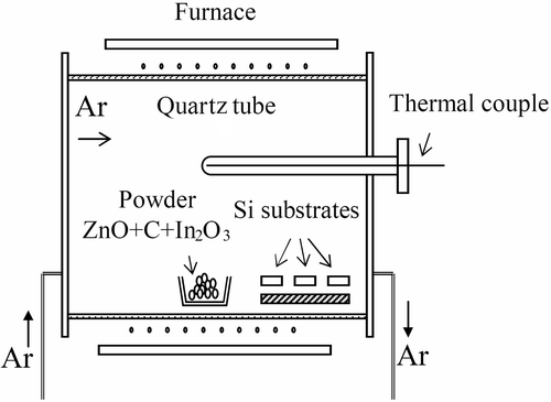
In-doped ZnO nanodisks were fabricated by thermal evaporation without catalyst. Our fabrication of ZnO nanodisks was conducted in a horizontal tube furnace. The system is shown in . The mixture of ZnO (purity 99.9%, 50 µm in size), In2O3 (purity, 99.9%, 50 µm in size), and graphite powders (purity 99.9%, 40 µm in size) with a mole ratio of 2 : 1 : 2 was placed in a ceramic boat inside a quartz tube as the evaporation source. Si (111) wafers were used as the substrates. The furnace temperature was set at 950°C in the growth process. There was a flat temperature zone (950°C) at the centre location of the furnace and the temperature gradient at the location between the centre and the end of the furnace was approximately 450°C. Ar was used as carrier gas. The flow rate of Ar was about 250–350 standard cubic centimetres per minute (sccm). A white product with some small slightly yellow region was obtained on the substrate.
Figure 1. Schema of the experiment.
The morphology and structure of the products were investigated by scanning electron microscopy (SEM) (JEOL-JSM5410 LV), high-resolution transmission electron microscopy TEM (HRTEM) (Hitachi H-9000NAR), X-ray diffraction (XRD) (Bruker-AXS D5005), and selected area electron diffraction (SAED). Photoluminescence (PL) measurements from 10 K to room temperature were carried out on a Fluorolog FL3-22 Jobin Yvon Spex USA with a Xe lamp as the excitation light source.
3. Results and discussion
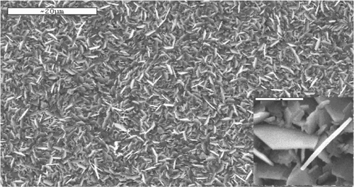
We have obtained densely populated In-doped ZnO disks on a Si substrate by thermal evaporation, as shown in . The disks are hexagons that have regular edges with an angle of 120° between adjacent sides, as demonstrated in the inset of . The disks are typically tens of nanometres in thickness and several microns in diameter.
Figure 2. SEM image of In-doped ZnO disks, (inset: magnified SEM image).
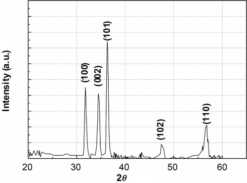
shows the XRD patterns of In-doped ZnO disks. It can be seen that the peaks in the pattern can be indexed to wurtzite structure. The strong diffraction peaks indicate high crystallinity of the ZnO disks. Analysis of the XRD shows lattice constant of a = 3.248 Å and c = 5.206 Å.
Figure 3. XRD pattern of In-doped ZnO disks.
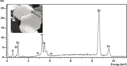
Energy dispersive spectroscopy (EDS) measurement confirms that the average In content in the disks defined as In/(Zn+In) atomic ratio, reaches 2.68 at.% ().
Figure 4. EDS of an In-doped ZnO nanodisk.
The TEM analysis gives us more details about the microstructure of the nanodisks, as shown in .
Figure 5. (a) TEM image of a hexagonal disk; (b) SAED pattern of ZnO nanodisk (c) high-resolution TEM image of a ZnO nanodisk taken along the electron beam perpendicular to surface of the nanodisk.
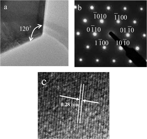
The nanodisks are of good transparency to the electron beam and the contrast on a whole disk is homogenous, which indicates that nanodisks are very thin and their surfaces are very flat, as observed by SEM.
Many nanodisks are rather regular hexagons. The SAED pattern has revealed that the nanodisks are of single crystal structure.
is the high-resolution TEM image of ZnO nanodisk. The lattice fringe and the corresponding electron diffraction pattern are all taken with the electron beam perpendicular to the surface of nanodisk. The fringe spacing is about 0.28 nm, corresponding to the crystallographic directions within the (0001) planes.
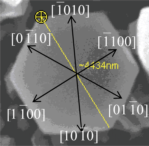
This indicates that the nanodisk grows mainly along the six symmetric directions of ,
, and
and the growth along [0001] is suppressed, as illustrated in .
Figure 6. The SEM image of a nanodisks with crystal orientations indicated.
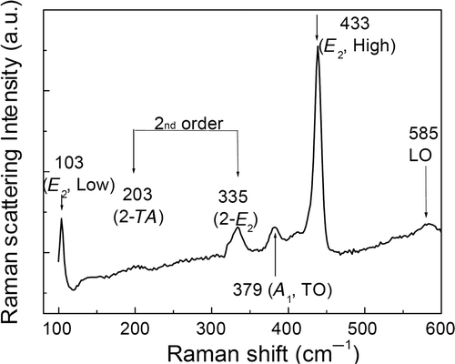
Further, Raman scattering, due to its sensitivity to the crystallisation, structural disorder, and defects in nanostructures, was measured for the ZnO nanodisks. shows their typical Raman spectrum. ZnO has a wurtzite crystal structure and belongs to C6v group. According to the analysis based on the group theory the A 1 + E 1 + 2E 2 modes are Raman active Citation6. Two high peaks at 103 and 433 cm−1 can be assigned to low and high E 2 mode, characteristic of the wurtzite lattice. Two weak peaks at 379 and 585 cm−1 are attributed to the transverse optical (TO) and longitudinal optical (LO) phonon mode of A 1 and E 1 symmetry, respectively. Two other weak and broad peaks at 203 and 335 cm−1 can be assigned to the second-order Raman scattering arising from zone-boundary phonons (2-TA(M), and 2-E 2(M), respectively) Citation7, and their appearence in the Raman spectra can relate to the oxygen deficiency in our ZnO nanodisks.
Figure 7. Raman scattering spectrum of the ZnO nanodisks.
The growth mechanism of the disks is not clear yet. In general, the nanostructured crystal of ZnO grows preferentially along [0001] direction, therefore, the nanowires are often obtained. The nanodisks can be obtained by suppressing the growth along c-axis in some conditions. The suppression effect is likely originated from Zn liquid droplets in a self-catalyzed vapour–liquid–solid process. The Zn vapour and In vapour generated by thermal carbon reduction of ZnO and In2O3 in the high temperature region transfer to the low temperature region and condense into liquid droplets and then are oxidised into ZnO nucleus with hexagonal facets. At the same time, Indium doping is achieved through the process of In substitute Zn atom in ZnO. If the (0001) facets of the crystallised ZnO are constantly kept clean and the newly incoming droplets can constantly wet and cover the entire condensed (0001) facet, the hexagonal In-doped ZnO disks can be obtained.
The PL measurements at low temperature were done for the ZnO nanodisks (). Most of PL spectra have a blue–green broad line and a group of ultraviolet (UV) narrow lines.
Figure 8. PL spectrum of ZnO–In nanodisks at 14 K.
The blue–green emission band was commonly attributed to a deep level (oxygen vacancies, interstitial zinc), trap-state, or surface state emission. Because, even at low temperature, ZnO : In is a nonstoichiometric oxide and presents deep defects such as oxygen vacancies, interstitial zinc Citation8.
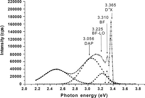
In this present work, we concentrate on investigation and explanation of origin of UV emission lines. The PL spectra of the ZnO nanodisks measured in the temperature range form 14 to 300 K are shown in .
Figure 9. The PL spectra measured at various temperatures of ZnO–In nanodisks.
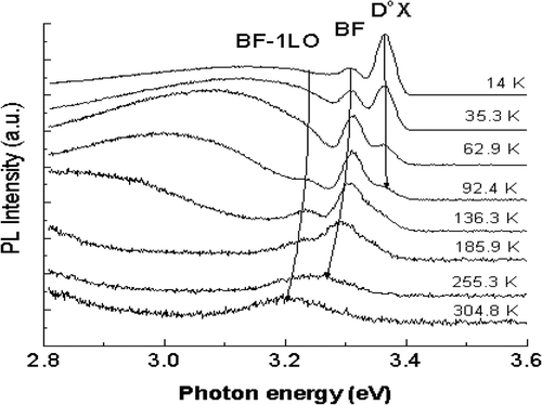
It can be seen that the PL spectra in the UV region exhibited one broad line at about 3.056 eV (denoted by line IV) and three narrow lines (lines III, II, I) at around 3.225 eV, 3.310 eV, 3.365 eV, respectively. As the temperature increases, these lines are shifted toward the low energy side, while their intensity decreases. The line I disappeared at temperature approximate to 166.1 K, whereas two lines II, III exist until room temperature.
In order to clarify the origins of emission lines, the experimental data were fitted by Gauss function:
Considering the temperature dependence of the lines I, II, III, we have found that the experimental values of line I are fitted rather well to the Varshini's semiempirical formula (2) Citation9:
Based on fitting results, the line I can be ascribed to a neutral donor-bound exciton (denoted by D°X).
The line II is still maintained up to room temperature and its position varies with temperature more slowly than the energy band gap. Thus, this line is attributed to the recombination of bound charge carriers on impurities with free carriers in the allowed bands (BF). In our case, the sample is an n-type semiconductor, so the line II can be the result of recombination between an electron bound on a donor and a free hole in the valence band (BF). The energy distance between two lines II and III at different temperatures is about 73 meV; this value is approximate to LO–phonon energy of 72 meV. Hence, the line III can be attributed to the phonon replica of the line II (BF–LO).
shows the integrated PL intensity of D°X and BF line as a function of temperature. It was found that the integrated PL intensity could be fitted by formula (3) Citation10:
Figure 10. The temperature dependence of integrated intensity of DoX and BF peaks.
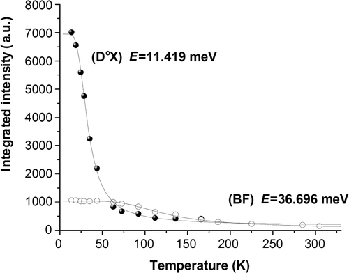
By curve fitting the experimental data in , we found that E = 11.4 meV and 36.7 meV for D°X and BF lines, respectively. The value of 11.4 meV is close to the value of the binding energy of the exciton bound to the neutral donors, experimentally obtained to be 12 meV Citation8. The value of 36.7 meV being larger than thermal activation energy at room temperature (∼26 meV) indicates possibility of existence of BF line at high temperatures.
The broad line at about 3.056 eV (line IV) is interpreted as a donor–acceptor pairs (DAP) emission. The position of DAP emission is described in Equation (Equation4):
With increasing temperature, carriers on donor–acceptor pairs with small distance r are released into the band, which results in extinguishing the high-energy side of DAP emission line, and the line is shifted to the low-energy side as observed in our experiment.
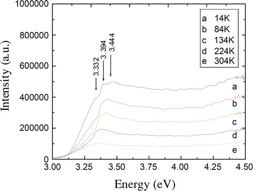
shows the photoluminescence excitation (PLE) spectra for the 2.43 eV (510 nm) emission line of ZnO–In nanodisks at different temperatures. At temperature 14 K, three peaks at 3.444, 3.394, and 3.332 eV are observed. With increasing temperature, the peaks are decreased in intensity and shifted to the lower energy side. The peak at 3.444 eV is attributed to the absorption of free exciton, the peak at 3.394 eV is assigned to the absorption of neutral donor-bound exciton and the peak at 3.332 eV is related to the transition from the valence band to donors.
Figure 11. PLE spectra of ZnO : In nanodisks.
4. Conclusion
Using a mixture of ZnO, In2O3, and graphite powder as source materials, In-doped nanometre thick disks were successfully fabricated by thermal evaporation without catalyst. The nanodisks are of single-crystal wurtzite structure and grow along the crystallographic directions within the {0001} planes. Both Raman and PL spectra proved that the ZnO–In nanodisks are of good crystalline and optical quality.
Acknowledgments
This work was supported financially by Fundamental Research Program, Ministry of Science and Technology of Vietnam (Project No. 40 55 06), and by Vietnam National University, Hanoi (Project No. QT 07 14).
References
- Liu , J , Zhang , Y , Qi , J , Huang , Y , Zhang , X and Liao , Q . 2006 . In-doped zinc oxide dodecagoral nanometer thick disks . Mater. Lett. , 60 : 2623 – 2626 .
- Cao , B , Cai , W , Li , Y , Sun , F and Zhang , L . 2005 . Ultraviolet-light-emitting ZnO nanosheets prepared by a chemical bath deposition method . Nanotechnology , 16 : 1734 – 1738 .
- Canh , TD , Tuyen , NV , Hoa , TTQ and Long , NN . 2005 . Fabrication and characterization of In-doped ZnO nanodisks , 1277 – 1280 . Hanoi : in Proceedings of the 6th National Conference of Physics .
- Lu , JG , Ye , ZZ , Huang , JY , Zhu , LP , Hao , BH , Wang , ZL and Fujta , SZ . 2006 . ZnO quantum dots synthesized by a vapor phase transports process . Appl. Phys. Lett. , 88 : 063110
- Tuyen , NV , Canh , TD , Long , NN and Hoa , TTQ . 2006 . Zinc/zinc oxide core/shell nanostructures, in Proceedings of the 1st IWOFM-3rd IWONN Conference , 396 – 399 . Viet Nam : Ha Long .
- Xu , CX , Sun , XW , Dong , ZL and Yu , MB . 2004 . Zinc oxide nanodisk . Appl. Phys. Lett. , 85 : 3878 – 3880 .
- Jie , J , Wang , G , Han , X , Yu , Q , Liao , Y , Li , G and Hou , JG . 2004 . Indium-doped Zinic oxide nanobelts . Chem. Phy. Lett. , 387 : 466 – 470 .
- Illy , B , Shollock , BA , Mac/hames-Driscoll , JL and Ryan , MP . 2005 . Electrochemical growth of ZnO nanoplates . Nanotechnology , 16 : 320 – 324 .
- Yan , Y , Liu , P , Wen , JG , To , B and Al-Jassim , MM . 2003 . In-situ Formation of ZnO Nano belts and Metallic Zn Nano betts and Nano disks . J. Phys. Chem. , 107 : 9701 – 9704 .
- Chi , DH , Binh , LTT , Binh , NT , Khanh , LD and Long , NN . 2006 . Band-edge photoluminescence in nanocrystalline ZnO: In films prepared by electrostatic spray deposition . Appl. Surface Sci. , 252 : 2770 – 2775 .