
ABSTRACT
Quaternary metal oxynitride-based photoanodes with a large light transmittance are promising for high solar-to-hydrogen (STH) conversion efficiency in photoelectrochemical (PEC) tandem cells. Transparent substrates to support PEC water-splitting were fabricated using atomic layer deposition (ALD) to synthesize 30 and 60 nm GaN on SiC substrates. A generalized approach was used to grow a quaternary metal oxynitride, i.e. SrTaO2N thin film on the GaN/SiC substrates. The transparency above 60% in the wide solar spectrum highlights its availability of transmitting visible light to the rear side. A photocurrent onset at ca. −0.4 V vs. reversible hydrogen electrode (RHE) was achieved by the SrTaO2N/GaN/SiC photoanodes in a 0.1 M NaOH electrolyte under simulated solar irradiation. This paves the way for the construction of hierarchically nanostructured tandem PEC cells. This work demonstrates the viability of integrating ALD in constructing substrates for semi-transparent quaternary metal oxynitride photoanodes.
GRAPHICAL ABSTRACT

1. Introduction
The development of effective solar-to-hydrogen (STH) systems is considered essential to alleviate the energy problem and establish a carbon-neutral society (Citation1–5). Photoelectrochemical (PEC) water splitting is potentially sustainable for large-scale conversion of solar energy into storable hydrogen source (Citation6–9). A technoeconomic report revealed that an STH efficiency above 10% is required for the practical application of PEC technology (Citation10, Citation11). While efficiencies have been improving over the past decades, enhanced sunlight utilization and circumvention from applying external voltage remain pressing issues, in addition to durability problems (Citation12–16). For the former, two fundamental losses are linked with low photoabsorbance. On one hand, most of the photon energy is lost with incident photons possessing energy lower than the bandgap (Eg); on the other hand, photons containing higher energy in comparison to Eg, are partially wasted by emitting phonons (Citation17, Citation18). The driving force for the latter is the required photovoltage (the potential difference between the quasi-Fermi levels of photogenerated electrons and holes), which is generally insufficient for a single photoelectrode to surmount the barriers associated with the kinetics needs (Citation19). In this regard, a self-biased PEC tandem cell powered only by solar energy is an ideal photoabsorber system to minimize the energy loss of the solar spectrum (Citation3, Citation17, Citation20). Sufficient photovoltage can be obtained to fulfill the energetic requirements, and higher potential states can be populated by both the excited electrons and holes to promote redox reactions (Citation10). A wireless tandem PEC cell, in which the photoanode and the photocathode are grown back to back, and separated by a visible-light-transparent and electrically conductive layer (TCL) are depicted in Scheme 1. Fabrication of this type of PEC device is desired due to its advantages in low photon and photovoltage losses and flexibility for industrial manufacture (Citation21, Citation22).
Scheme 1. Scheme of a wireless stand-alone PEC tandem cell.
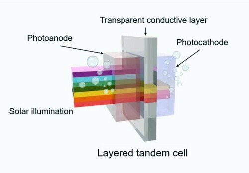
In particular, high transparency and efficiency of the front photoanode are critical prerequisites for achieving satisfied STH efficiency (Citation22). The photoanode has to transmit sunlight with a wavelength longer than its absorption edge to the rear side for reutilization by the photocathode (Scheme 1). The extensively exploited TiO2, ZnO, BiVO4-based photoanodes have been assembled to fabricate PEC tandem cells with diverse photocathodes (Citation22, Citation23). To achieve the STH efficiency of 10%, however, transparent photoanodes are required to spread their optical absorption spectra to the visible region, which accounts for a large portion of the solar spectrum (Citation10). It should be noted that the first photoanode in the optical pathway with high transparency for illumination below its band gap is also a prerequisite for dual-photoanode cells, which have advantages in achieving complementary light absorption and improving the STH efficiency (Citation17).
Compared with the best-performing oxidic photoanodes, i.e. BiVO4, nitrogen-containing compounds, such as metal nitrides and metal oxynitrides (1.7−2.4 eV), exhibit narrower bandgaps (Citation24). Recently, a relatively high STH efficiency was recorded using a Ta3N5 photoanode-involved tandem cell (Citation25). The transparent Ta3N5 on GaN/Al2O3 demonstrated high transparency of greater than 70% at wavelength above 600 nm, and gave an initial STH efficiency above 7% when combined with serially-connected dual-CuInSe2-based photocathodes for hydrogen production (Citation25). One key advantage of quaternary metal oxynitrides over Ta3N5 is their theoretically higher light absorption due to narrower band gaps, such as those found for SrTaO2N or SrNbO2N (Citation19). The occurrence of more cathodic photocurrent onsets is also generally observed in oxynitride-driven systems, which makes them being very attractive photoanode candidates for tandem PEC cell (Citation19, Citation21, Citation26).
Nonetheless, the fabrication process of transparent oxynitride thin films is demanding in comparison to oxides. Transparent quaternary oxynitride films have been previously obtained by pulsed laser deposition (PLD) (Citation27, Citation28), reactive radio frequency (RF) magnetron sputtering (Citation29–32), and spin-coating in conjunction with post-ammolysis (Citation21). Although several TCL substrates have been tested, including MgO, Al2O3, and SrTiO3 (Citation21, Citation32), the limited choices hamper the widespread application of transparent oxynitride-based photoanodes in tandem cell. This is because of the high temperatures and reducing atmosphere required in these processes. The frequently used indium tin oxides (ITOs) and fluorine-doped tin oxides (FTOs) substrates are not stable under ammonolysis and lose transparency, i.e. tin oxide is reduced to metallic tin (Citation33). An alternative substrate is silicon carbide (SiC), which is used for the deposition of electronic grade GaN in high-frequency electronics due to its extremely good thermal conductivity (Citation34).
For TCL substrates, a current collector overlayer, e.g. GaN and TiN, is required to enable the transport of photogenerated electrons (Citation25, Citation28). The high electron mobility of the former makes it a key material in advanced AlGaN/GaN high electron mobility transistors (exceed 1000 cm2 V−1 s−1) (Citation35, Citation36). Insertion of an interlayer between the photoanode films and the TCL could also mitigate the charge recombination by energetic alignment of the band edges (Citation10, Citation37). This was observed when a 150-nm GaN layer was deposited between a Ta substrate and Ta3N5 film by plasma-enhanced chemical vapor deposition (PCVD), which led to a 1.8-fold enhancement in water oxidation efficiency (Citation37). However, it is difficult to deposit GaN directly onto SiC by chemical vapor deposition (CVD) due to poor wetting of the film on the substrate (Citation38). Furthermore, high temperatures (600−1000°C) are often used for CVD-GaN (Citation39, Citation40), which is unsuitable for heat-sensitive films (e.g. InN, decomp. 500°C) (Citation41).
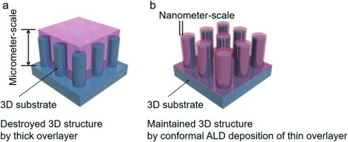
Deposition of thin films with excellent uniformity and conformity, and controlled thickness is essential for the fabrication of solar devices with complex surface architecture (Citation42). These pre-requirements, however, cannot be fulfilled by CVD, especially for three-dimensional (3D) TCL substrates (Citation43, Citation44). A thick coating on the surface is prone to fill the trenches and/or holes (Scheme 2a), which is adverse for interfacial reactions. These aspects, therefore, highlight the importance of atomic layer deposition (ALD) due to its self-limiting growth mechanism for realizing future hierarchically nanostructured metal oxynitride photoanodes (Citation38, Citation45, Citation46). It should be noted that GaN layers with thickness less than 100 nm were also demonstrated in several reports to be capable of charge transfer in solar energy devices (Citation47–49). This is important for us to allow the deposition of the current collector layer to be governed readily by ALD in a low-temperature regime and to simultaneously maintain structural conformity (Scheme 2b) (Citation50). Motivated by these conditions, we were interested to examine the viability of the ALD GaN layer on 4H−SiC for constructing transparent quaternary oxynitride photoanodes. The examination of thickness influence of GaN is meaningful to understand the critical limit required for the fabrication of quaternary oxynitride film on 3D transparent substrates.
Scheme 2. Schematic illustration of the crucial role ALD plays in achieving semi-transparent hierarchically structured quaternary oxynitride photoanodes. 3D substrates are covered by (a) thick and (b) conformal GaN overlayers. Previous reports using metalorganic vapor phase epitaxy deposition (MOVPE) for GaN deposition led to a micrometer coating that results in the loss of nanostructured textures. Realizing GaN fabrication via ALD on SiC would enable to maintain the high surface area.
In this work, we fabricated planar n-type GaN-coated SiC substrates using ALD and subsequently synthesized SrTaO2N oxynitride thin film photoanodes. The oxynitride layers prepared on GaN/SiC exhibited significant transparency in almost the whole solar spectrum and a very negative onset potential of photoresponse.
2. Experimental
2.1. Preparation of SiC/GaN transparent substrates
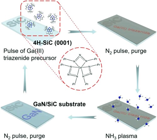
GaN thin films were deposited epitaxially on polished single crystal 4H−SiC (0001) substrates by ALD (Citation38). A highly volatile tris(1,3-diisopropyltriazenide)gallium(III) precursor, (Ga(triaz)3), was used as the Ga source. This is due to the low carbon impurities and high stoichiometry of the final GaN film (Ga/N ratio: 1.05) (Citation38). The detailed synthetic procedure of the Ga(III) triazenide precursor is provided in our previous reports (Citation38, Citation42).
Prior to the deposition, the 4H−SiC substrates were cleaned in solutions of [1:1:5 solution of H2O2 (30%), NH3 (25%), and H2O] and [1:1:5 solution of H2O2 (30%), HCl (37%), and H2O] to remove potential organic and inorganic contaminants. A hot-wall Picosun R-200 equipped with a Litmas remote plasma source was used for the deposition. The system flowing with N2 (99.999%, 300 mL min−1) was heated at 450°C for 2 h to remove the trace amount of residual H2O and O2 in the deposition chamber due to the air contaminant during substrate exchange. Inside a N2-filled glovebox, ∼1.0 g of the Ga(III) triazenide precursor (per 1000 ALD cycles) was transferred into a glass vial and placed into a stainless steel container (bubbler). It was then assembled into the system and the temperature for the bubbler was adjusted to 130°C. A dried gas mixture containing NH3 (99.999%) and Ar (99.9997%) in the ratio of 75/100 was introduced as NH3 plasma with a 2800 W plasma power, which was located ca. 75 cm above the SiC substrate. A 10 s pulse of Ga(III) triazenide precursor and 12 s NH3 plasma were used for each cycle of deposition, separated by a 10-s pulse of N2. The base pressure of the ALD reactor under carrier gas flow is 5 hPa, while a slight increase in the reactor pressure up to 7 hPa can be seen during the precursor pulse. This process was conducted at 350°C (growth rate: 0.3 Å/cycle) to yield 30 and 60 nm of epitaxial GaN on 4H−SiC (Citation38). The obtained substrates were finally diced into 1 × 2 cm2 pieces and well stored for further use.
2.2. Fabrication of SrTaO2N thin films on SiC/GaN transparent substrates
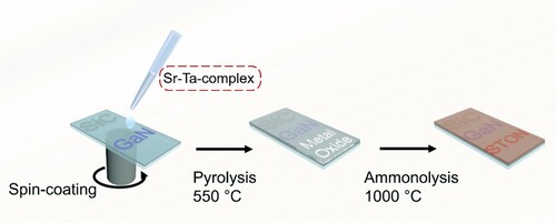
Quaternary SrTaO2N thin films were prepared by ammonolysis of the corresponding metal–oxide layers at elevated temperature. A modified polymerized-complex (PC) method was applied to prepare the precursor solution with follow-up spin-coating to give metal-complex layer (Citation51–53). In a typical synthesis, 200 mg TaCl5 (Sigma-Aldrich, 99.8%) and 858 mg citric acid (Sigma-Aldrich, > 99%) were dissolved in 2 mL ethylene glycol (Sigma-Aldrich, > 99%) under vigorous stirring to produce the Ta-complex solution. An inert atmosphere was used during the preparation. A solution of 118 mg Sr(NO3)2 (Sigma-Aldrich, > 99%) in 0.2 mL deionized water, dissolved using ultrasonication, was then slowly injected into the aforementioned complex solution and the setup was kept at 70°C during the process. The mixture was subsequently heated to 100°C and magnetically stirred for 30 min. The resultant viscous solution was used to prepare the thin film on the GaN/SiC substrate by spin-coating at 2000 rpm for 3 min in air. It was baked afterwards at 150 and 300°C for 30 min each in sequence to promote polymerization. The obtained sample was calcinated at 550°C for 2 h to remove organic components and to give the metal oxide precursor. The substrate was transferred into an alumina boat and mounted in a tube furnace for nitridation at 1000°C for 2 h under flowing NH3 (30 mL min−1) and H2 (5 mL min−1), with the ramping rate of 7°C min−1. The transparent SrTaO2N film on GaN/SiC substrate was finally obtained after cooling down to room temperature.
In addition, a particle-based SrTaO2N photocathode was also made as contrast by the Electrophoretic deposition (EPD) method. In brief, two FTO glasses (1.5 × 3 cm2) with the distance of 1 cm were vertically immersed into 20 mL acetone solution dispersing with 20 mg SrTaO2N powder and 7 mg iodine. The powder oxynitride was prepared via the same route to the aforementioned thin film sample, but without the spin-coating process. Constant DC bias of 20 V was applied between the FTO substrates for 3 min, after which the electrode was allowed for volatilization of iodine overnight before measurement.
2.3. Characterization
Phase structure was analyzed in transmission mode by using a calibrated STOE STADI-P powder X-ray diffractometer (PXRD) with a flat sample holder and Cu Kα1 radiation (2θ range 5−120°, with individual steps of 0.01°). Powder sample prepared from the same precursor solution and identical ammonolysis process was used for the measurement. Scanning electron microscope (SEM, Leo Supra 35VP SMT, Zeiss) was used to scrutinize the surface morphology of the photoanodes. UV–vis transmittance spectra were recorded by using a UV–vis spectrophotometer (Shimadzu, UV-2600). The GaN films were comparable to the previously reported films by this ALD process in terms of thickness and crystallinity, detailed characterization information can be found in reference Citation38.
2.4. Photoelectrochemical measurements
PEC experiments were performed under simulated solar illumination, which was generated by an Air Mass 1.5 Global solar light simulator (AM 1.5G, 100 mW cm−2, class-AAA 94023A, Newport) with an ozone-free 450 W Xenon short-arc lamp. The measurements were conducted in 0.1 M NaOH solution (pH∼13) with a three-electrode PEC cell, in which the SrTaO2N/GaN/SiC photoanode, 1 M Ag/AgCl electrode, and Pt electrode were used as the working electrode, the reference electrode, and the counter electrode, respectively. 0.1 M Na2SO3 as a hole scavenger was introduced into the electrolyte if mentioned. CoFeOx as an oxygen evolution catalyst was electrodeposited on the surface of the photoanodes according to a reported protocol (Citation54). Electrodeposition was operated in the aforementioned three-electrode cell by unidirectional sweeping voltage from 1.35 to 1.65 VRHE for 3 cycles. The electrodeposition electrolyte was comprised of 10 mM FeCl3·6H2O (Sigma Aldrich, >98%), 16 mM CoCl2 (Sigma Aldrich, >98%) and 0.1 M NaOAc (Sigma Aldrich, 99%) in deionized water, without adjusting pH.
The applied potentials were ultimately converted into the scale of reversible hydrogen electrode (RHE) with Nernst equation (ERHE = E0Ag/AgCl + 0.059 V × pH + EAg/AgCl) (Citation9). Linear sweep voltammetry (LSV) at a scan rate of 10 mV s−1 and Chronoamperometry (CA) at 1.23 VRHE were measured with a potentiostat (PalmSens4, PalmSens BV) under interrupted AM 1.5G illumination with an interval of 5 s. Mott−Schottky experiments were operated with an amplitude of 10 mV in dark condition.
3. Results and discussion
3.1. Synthesis
The GaN layer was deposited epitaxially on 4H–SiC pieces by ALD without the use of an AlN nucleation buffer layer (Scheme 3). A hexacoordinated Ga−N bonded precursor we synthesized recently, Ga(triaz)3, was employed as the Ga source (Citation38). This precursor was demonstrated to be an excellent ALD precursor for high-quality GaN (Citation38). ALD of GaN was implemented on SiC substrates by using an ALD cycle with alternating pulses of the Ga(III) triazenide precursor and NH3 plasma separated by N2 purges. The films were deposited at 350°C to produce 30 and 60 nm of epitaxial GaN on 4H–SiC, respectively.
Scheme 3. Schematic illustration of the ALD cycle used to deposit GaN on 4H–SiC.
A spin-coating step was conducted to homogeneously adsorb precursor sol containing Sr and Ta onto the substrates (Scheme 4). The complex sol was prepared by a PC method due to the homogeneity of the metal species inside the organic network (Citation55). After calcination in air and subsequent nitridation in NH3 atmosphere, stoichiometric SrTaO2N photoanodes with high transparency were formed.
Scheme 4. Schematic diagram of the fabrication procedure for transparent quaternary SrTaO2N thin film photoelectrode on GaN/SiC substrate. The direct synthesis was adopted by the use of the Sr–Ta-complex as the precursor solution through a spin-coating procedure and subsequent thermal treatments.
3.2. Structure and optical property
To analyze the crystal structure of the resultant oxynitride, PXRD patterns were collected (a) and confirmed the single-phase crystallographic purity of SrTaO2N. The diffraction peaks are in agreement with the ICSD entry 130056 (Citation56).
Figure 1. (a) PXRD patterns of SrTaO2N. (b) and (c) Digital photos of oxide-precursor film and SrTaO2N film, respectively. SEM images of the SrTaO2N films on (d) 30 nm GaN/SiC and (e) 60 nm GaN/SiC.
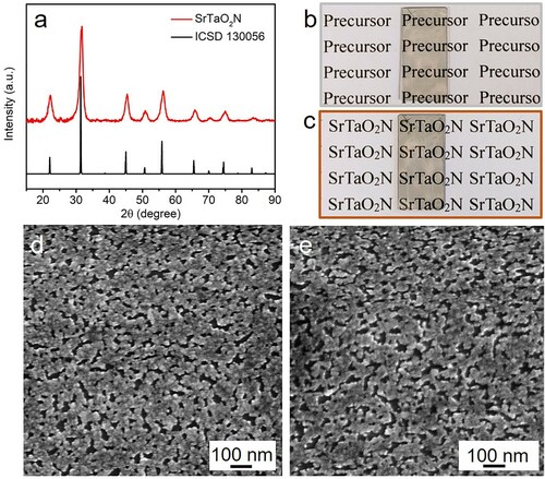
Panels b and c of correlate the digital photos of the 30 nm GaN/SiC substrates overlayed with metal oxide precursor and SrTaO2N thin film, respectively. Very thin and transparent layers were deposited on the substrate after pyrolyzing the spin-coated sample. Subsequent nitridation in ammonia atmosphere introduced a slight brownish hue on the surface while still preserving high transparency. The top-view SEM images of the prepared SrTaO2N thin films on 30 and 60 nm GaN/SiC are presented in (d) and (e), respectively, where the SrTaO2N thin films composed of numerous closely packed irregular nanoparticles with an average diameter lower than 100 nm. The noticeable interspace between the oxynitride grains was most likely caused by the pyrogenic decomposition of the organic skeleton in the complex. This morphological structure has been detected in related ceramic films prepared by spin-coating with metal-complex sol in conjunction with a high-temperature pyrolysis (Citation21, Citation57–59). Compared with bare GaN/SiC substrate (Figure S1), a surface morphology variation can be noticed by SrTaO2N. Figure S2 correlates the cross-sectional SEM image of the SrTaO2N/60 nm GaN/SiC, where the constituent layers and corresponding interfaces can be identified and the thickness of this SrTaO2N film is ca. 364 nm.
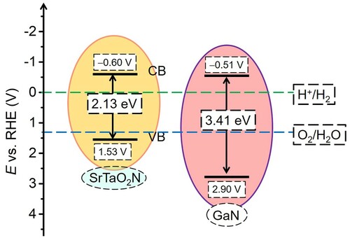
The prepared SrTaO2N thin films on GaN (30 and 60 nm thickness) exhibit high transparency (a). The UV–vis measurement indicates that the transmittance of the photoanodes is greater than 60% in almost the whole solar spectrum. Only a slight difference is inspected in comparison with the pristine GaN/SiC substrate. This is ascribed to the limited deposition content of the oxynitride on the surface, which is also linked to the absence of discernible photoabsorption edge at ca. 550 nm of SrTaO2N. This high transparency has the potential to allow for the construction of a dual photoanode cell or a tandem PEC cell by integrating with another photoelectrode (Citation17, Citation21, Citation25). Due to the high transmittance of the thin film electrodes, the band gap of the SrTaO2N was evaluated based on the prepared powder sample to be 2.13 eV from Kubelka–Munk-transformed reflectance spectrum, as presented in (b). Since the band edge alignment is essential for effective charge transfer across the interface in laminated photoelectrodes, Mott–Schottky experiments were implemented to acquire the detailed band structures (c). The flat band potential (Efb) of the SrTaO2N electrode was determined to be ca. −0.40 VRHE, being consistent with the previous reported potential range (Citation51, Citation60). The n-type nature of the film is also confirmed by the positive slops of the Mott–Schottky curves (Citation61, Citation62). Given that the bottom potential of conduction band (ECB) is generally considered to be 0.2 V above the Efb (Citation63), the ECB is therefore populated at ca. −0.60 VRHE for the SrTaO2N. Based on the documented band gap value, the band edge positions of the SrTaO2N photoanode are depicted in . In addition, the electronic band structure of the underlying GaN layer is also scrutinized according to the recorded band gap of 3.41 eV in our earlier report and the detected Efb of −0.31 VRHE by complementary Mott–Schottky measurement (d). Due to the staggered band edge structures, a type II heterojunction interface is therefore established by depositing SrTaO2N on GaN. The driving force afforded by the gradient band energy structure is qualified to allow for spatial charge separation, during which the holes accumulated on the oxynitride film can participate in water oxidation on surface, whereas the electrons are driven backward to the counterelectrode (Citation64).
Figure 2. (a) UV–vis transmittance spectra of the samples (insets exhibit the photographic images of the films). (b) Kubelka–Munk-transformed reflectance spectrum of SrTaO2N. Mott–Schottky plots of (c) SrTaO2N and (d) GaN. For Mott–Schottky measurement, the SiC side and the edge of the substrate were insulated with insulation paste to eliminate the potential interference from SiC.
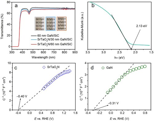
Figure 3. Schematic illustration of the electronic band structures of SrTaO2N and GaN layers.
3.3. Photoelectrochemical water oxidation
The PEC water oxidation performance was evaluated in alkaline media (0.1 M NaOH solution) with a three-electrode configuration (a). LSV curves measured at 10 mV s−1 were recorded under interrupted illumination with increasing potential bias (b). The generated electronic current in the presence of irradiation is the photocurrent, which is proportional to the amount of H2 and O2 produced (Citation28). The discernible anodic photocurrent of SrTaO2N thin film on 30 nm GaN layer emerges at ca. −0.4 VRHE, indicative of a very negative onset of photoresponse. The detected net photocurrent densities for this electrode are comparable in the wide potential range, i.e. 0.2−1.4 VRHE, despite the consecutive increment in the applied potentials. A similar phenomenon was also identified in a 500 nm Ta3N5 thin film photoanode, which was fabricated from RF magnetron sputtering of Ta precursor on 4 μm Si-doped GaN fixed on a sapphire substrate (Citation25). This result is mainly attributed to the limited thickness of the oxynitride thin film on the substrate confining the availability of sufficient active sites (Citation30, Citation65). The photocurrent density derived from photoexcited charge carriers is therefore already saturated at low potential bias during the LSV measurement. The net photocurrent density generated by this SrTaO2N thin film was approximately 6 μA cm−2 at 1.23 VRHE (c). This photocurrent density is expected due to the incompatibility between high transparency and immense photocurrent density for a single-component photoelectrode. Nevertheless, it is commensurate with the values reported for a 150-nm SrTaO2N film photoanode grown on Ta sheet by reactive RF magnetron sputtering (Citation30). In this report, the enhanced photocurrent was observed upon expanding the film thickness by adjusting the sputtering duration (Citation30). The PEC performance of as-prepared photoanode is compared with some representative references in , the recorded photoresponse onset (−0.4 VRHE) highlights the advantage of the obtained photoanode. Given that this photocurrent density is also higher than a 162 nm LaTiO2N and a 177 nm CaNbO2N thin film photoanodes prepared by a modified PLD method on a TiN layer with (001)-oriented supporting MgO, in which photocurrent density less than 1 μA cm−2 was recorded at 1.23 VRHE () (Citation65). In this regard, the present result is promising and the performance is likely to be further improved by extending the oxynitride film thickness and to apply to porous 3D substrates. It is noteworthy that these post modifications would inevitably reduce the transmittance in varied degrees and an equilibrium that maintains luminousness while allows for high photocurrent density deserves further research.
Figure 4. (a) Scheme of the PEC water splitting cell. (b) LSV and (c) CA curves at 1.23 VRHE of SrTaO2N/GaN/SiC photoanodes and bare substrate recorded under interrupted AM 1.5G illumination in 0.1 M NaOH electrolyte. (d) Schematic illustration of the hole transfer path in the laminated structure for water oxidation.
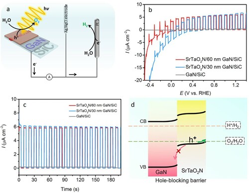
Table 1. Comparison to previously published thin film-based quaternary oxynitride photoanodes.
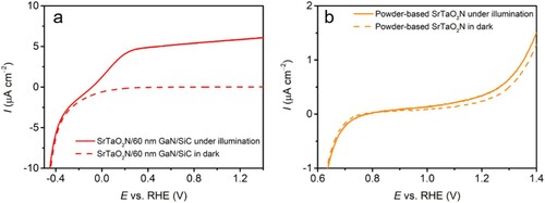
To elucidate the photoelectrode performance based on the thickness of the GaN layer, the SrTaO2N thin film was grown identically on a 60-nm epitaxial GaN on the 4H–SiC substrate (Schemes 3 and 4). This electrode displays a very similar performance to the SrTaO2N photoanode with a 30 nm GaN underlayer in both LSV and CA (b and c). This means that 30 nm GaN is already adequate to allow for effective charge transport. Since a bare GaN/SiC substrate does not present noticeable photoresponse, it excludes the photocurrent contribution from the substrate in the SrTaO2N photoanodes. Nevertheless, the insertion of a thin GaN film between the photoanode material and the SiC substrate is critical to supplying the pronounced photoresponse (vide infra) (Citation25, Citation37). A particle-based SrTaO2N photoanode was also prepared by the EPD method, which is compared with the SrTaO2N thin film in . In comparison with the particle-based electrode, SrTaO2N thin film photoanode demonstrates substantially higher photocurrent and lower dark current, which indicates the better PEC behavior of the latter. We have recently introduced a 2-μm GaN layer on sapphire substrates by MOVPE, which was used for SrTaO2N and LaTiO2N thin film deposition (Citation21). Although the fabricated photoanodes demonstrated comparable photocurrent density with the present SrTaO2N thin film, the pronounced cathodic shift of the onset potential and the far smaller thickness of the GaN highlight the significance of the Ga(III) triazenide precursor and ALD technique in producing high-quality GaN conductive layer. In addition, the SrTaO2N/60 nm GaN/SiC and SrTaO2N/30 nm GaN/SiC photoanodes exhibit 1.9- and 1.7-fold improvements, respectively, in photocurrent density at 1.23 VRHE by introducing Na2SO3 as hole scavenger into the electrolyte (Figure S3). Surface modification with CoFeOx catalyst also leads to a 1.7- and 1.5-fold improvements in photocurrent density for SrTaO2N/60 nm GaN/SiC and SrTaO2N/30 nm GaN/SiC photoanodes, respectively (Figure S4).
Figure 5. LSV curves of (a) SrTaO2N/60 nm GaN/SiC and (b) particle-based SrTaO2N photoanodes.
In addition to the mitigation in conductivity, the GaN layer inserted between the SrTaO2N and SiC also sustains hole-blocking effect to alleviate carrier recombination (25, 37, 67, 68). This effect is similar to a reported SnO2 layer for BiVO4 thin film, and a Lu2O3 film deposited on a BiVO4 photoanode (Citation69, Citation70). The introduced GaN that can afford hole-blocking potential barrier is prone to suppress the backward holes migration from the photoabsorber, due to its deep position on the top of the valance band (d). The relative thin thicknesses of GaN and SrTaO2N are also conductive to mitigate the recombination of photogenerated electrons and holes, owing to the short transfer path to the interfaces of SrTaO2N/GaN and electrolyte/SrTaO2N, respectively (Citation65).
4. Conclusions and outlook
In summary, we have demonstrated ALD grown GaN on SiC can be used as transparent substrates for constructing semi-transparent SrTaO2N/GaN/SiC photoanodes. The absence of a buffer layer for initial GaN film growth, the high-quality GaN, and the ease of the SrTaO2N thin film displays the practicability of this process for large-scale manufacture. The formation of alternative semi-transparent quaternary metal-based oxynitride photoanodes, especially for semi-transparent hierarchically structured photoanodes, would be feasible with this new process.
The excellent light transmittance and remarkably negative onset potential validated the potential of the synthesized photoanodes to work as front photoelectrode in constructing stand-alone tandem PEC devices. Despite the low photocurrent of the planar photoanodes with respect to the theoretical value, the GaN underlayer grown via ALD paves the way toward the fabrication of hierarchically-ordered three-dimensional semi-transparent quaternary oxynitride photoanodes. Work toward this direction is currently on-going in our laboratory.
Supplemental Material
Download MS Word (494.9 KB)Acknowledgments
This work was financially supported by the Swedish Energy Agency (project no. 50501-1) and by the Swedish Foundation for Strategic Research through the project ‘Time-resolved low temperature CVD for III-nitrides’ (SSF-RMA 15-0018). Can Lu appreciates the China Scholarship Council (CSC) for a Ph.D. scholarship. We thank Professor Ulrich Simon for access to scanning electron microscopy facilities.
Disclosure statement
No potential conflict of interest was reported by the author(s).
Additional information
Funding
References
- Ma, Z.; Thersleff, T.; Görne, A.L.; Cordes, N.; Liu, Y.; Jakobi, S.; Rokicinska, A.; Schichtl, Z.G.; Coridan, R.H., Kustrowski, P., et al. Quaternary Core–Shell Oxynitride Nanowire Photoanode Containing a Hole-Extraction Gradient for Photoelectrochemical Water Oxidation. ACS Appl. Mater. Interfaces 2019, 11 (21), 19077–19086.
- Lu, C.; Ma, Z.; Jäger, J.; Budnyak, T.M.; Dronskowski, R.; Rokicińska, A.; Kuśtrowski, P.; Pammer, F.; Slabon, A. NiO/Poly(4-Alkylthiazole) Hybrid Interface for Promoting Spatial Charge Separation in Photoelectrochemical Water Reduction. ACS Appl. Mater. Interfaces 2020, 12 (26), 29173–29180.
- Ben-Naim, M.; Britto, R.J.; Aldridge, C.W.; Mow, R.; Steiner, M.A.; Nielander, A.C.; King, L.A.; Friedman, D.J.; Deutsch, T.G., Young, J.L., et al. Addressing the Stability Gap in Photoelectrochemistry: Molybdenum Disulfide Protective Catalysts for Tandem III-V Unassisted Solar Water Splitting. ACS Energy Lett 2020, 5, 2631–2640.
- Oshima, T.; Nishioka, S.; Kikuchi, Y.; Hirai, S.; Yanagisawa, K.; Eguchi, M.; Miseki, Y.; Yokoi, T.; Yui, T., Kimoto, K., et al. An Artificial Z-Scheme Constructed from Dye-Sensitized Metal Oxide Nanosheets for Visible Light-Driven Overall Water Splitting. J. Am. Chem. Soc 2020, 142 (18), 8412–8420.
- Meng, L.; Wang, M.; Sun, H.; Tian, W.; Xiao, C.; Wu, S.; Cao, F.; Li, L. Designing a Transparent CdIn2S4/In2S3 Bulk-Heterojunction Photoanode Integrated with a Perovskite Solar Cell for Unbiased Water Splitting. Adv. Mater 2020, 32 (30), 2002893.
- He, Y.; Hamann, T.; Wang, D. Thin Film Photoelectrodes for Solar Water Splitting. Chem. Soc. Rev 2019, 48 (7), 2182–2215.
- Wang, Q.; Domen, K. Particulate Photocatalysts for Light-Driven Water Splitting: Mechanisms,: Challenges, and Design Strategies. Chem. Rev 2020, 120 (2), 919–985.
- Wang, Z.; Li, C.; Domen, K. Recent Developments in Heterogeneous Photocatalysts for Solar-Driven Overall Water Splitting. Chem. Soc. Rev 2019, 48 (7), 2109–2125.
- Lu, C.; Drichel, A.; Chen, J.; Enders, F.; Rokicińska, A.; Kuśtrowski, P.; Dronskowski, R.; Boldt, K.; Slabon, A. Sensibilization of p-NiO with ZnSe/CdS and CdS/ZnSe Quantum Dots for Photoelectrochemical Water Reduction. Nanoscale. 2021, 13 (2), 869–877.
- Kawase, Y.; Higashi, T.; Domen, K.; Takanabe, K. Recent Developments in Visible-Light-Absorbing Semitransparent Photoanodes for Tandem Cells Driving Solar Water Splitting. Adv. Energy Sustain. Res 2021, 2 (7), 2100023.
- Pinaud, B.A.; Benck, J.D.; Seitz, L.C.; Forman, A.J.; Chen, Z.; Deutsch, T.G.; James, B.D.; Baum, K.N.; Baum, G.N., Ardo, S., et al. Technical and Economic Feasibility of Centralized Facilities for Solar Hydrogen Production via Photocatalysis and Photoelectrochemistry. Energy Environ. Sci 2013, 6 (7), 1983–2002.
- Kim, J.H.; Hansora, D.; Sharma, P.; Jang, J.W.; Lee, J.S. Toward Practical Solar Hydrogen Production-an Artificial Photosynthetic Leaf-to-Farm Challenge. Chem. Soc. Rev 2019, 48 (7), 1908–1971.
- Deng, J.; Su, Y.; Liu, D.; Yang, P.; Liu, B.; Liu, C. Nanowire Photoelectrochemistry. Chem. Rev 2019, 119 (15), 9221–9259.
- Ku, C.; Wu, P.; Chung, C.; Chen, C.; Tsai, K.; Chen, H.; Chang, Y.; Chuang, C.; Wei, C., Wen, C., et al. Creation of 3D Textured Graphene/Si Schottky Junction Photocathode for Enhanced Photo-Electrochemical Efficiency and Stability. Adv. Energy Mater 2019, 9 (29), 1901022.
- Wang, D.Y.; Li, C.H.; Li, S.S.; Kuo, T.R.; Tsai, C.M.; Chen, T.R.; Wang, Y.C.; Chen, C.W.; Chen, C.C. Iron Pyrite/Titanium Dioxide Photoanode for Extended Near Infrared Light Harvesting in a Photoelectrochemical Cell. Sci. Rep 2016, 6 (1), 20397.
- Wang, W.; Xu, M.; Xu, X.; Zhou, W.; Shao, Z. Perovskite Oxide Based Electrodes for High-Performance Photoelectrochemical Water Splitting. Angew. Chem. Int. Ed 2020, 59 (1), 136–152.
- Kim, J.H.; Jang, J.-W.; Jo, Y.H.; Abdi, F.F.; Lee, Y.H.; van de Krol, R.; Lee, J.S. Hetero-Type Dual Photoanodes for Unbiased Solar Water Splitting with Extended Light Harvesting. Nat. Commun 2016, 7 (1), 13380.
- Guo, F.; Li, N.; Fecher, F.W.; Gasparini, N.; Quiroz, C.O.R.; Bronnbauer, C.; Hou, Y.; Radmilović, V.V.; Radmilović, V.R., Spiecker, E., et al. A Generic Concept to Overcome Bandgap Limitations for Designing Highly Efficient Multi-Junction Photovoltaic Cells. Nat. Commun 2015, 6 (1), 7730.
- Seo, J.; Nishiyama, H.; Yamada, T.; Domen, K. Visible-Light-Responsive Photoanodes for Highly Active, Stable Water Oxidation. Angew. Chem. Int. Ed 2018, 57 (28), 8396–8415.
- Cheng, W.-H.; Richter, M.H.; May, M.M.; Ohlmann, J.; Lackner, D.; Dimroth, F.; Hannappel, T.; Atwater, H.A.; Lewerenz, H.-J. Monolithic Photoelectrochemical Device for Direct Water Splitting with 19% Efficiency. ACS Energy Lett 2018, 3 (8), 1795–1800.
- Ma, Z.; Piętak, K.; Piątek, J.; Reed DeMoulpied, J.; Rokicińska, A.; Kuśtrowski, P.; Dronskowski, R.; Zlotnik, S.; Coridan, R.H.; Slabon, A. Semi-Transparent Quaternary Oxynitride Photoanodes on GaN Underlayers. Chem. Commun 2020, 56 (86), 13193–13196.
- Chen, Y.; Feng, X.; Liu, Y.; Guan, X.; Burda, C.; Guo, L. Metal Oxide-Based Tandem Cells for Self-Biased Photoelectrochemical Water Splitting. ACS Energy Lett 2020, 5 (3), 844–866.
- Jiang, C.; Moniz, S.J.A.; Wang, A.; Zhang, T.; Tang, J. Photoelectrochemical Devices for Solar Water Splitting-Materials and Challenges. Chem. Soc. Rev 2017, 46 (15), 4645–4660.
- Takata, T.; Pan, C.; Domen, K. Design and Development of Oxynitride Photocatalysts for Overall Water Splitting Under Visible Light Irradiation. ChemElectroChem 2016, 3 (1), 31–37.
- Higashi, T.; Nishiyama, H.; Suzuki, Y.; Sasaki, Y.; Hisatomi, T.; Katayama, M.; Minegishi, T.; Seki, K.; Yamada, T.; Domen, K. Transparent Ta3N5 Photoanodes for Efficient Oxygen Evolution Toward the Development of Tandem Cells. Angew. Chem. Int. Ed 2019, 58 (8), 2300–2304.
- Ma, Z.; Jaworski, A.; George, J.; Rokicinska, A.; Thersleff, T.; Budnyak, T.M.; Hautier, G.; Pell, A.J.; Dronskowski, R., Kuśtrowski, P., et al. Exploring the Origins of Improved Photocurrent by Acidic Treatment for Quaternary Tantalum-Based Oxynitride Photoanodes on the Example of CaTaO2N. J. Phys. Chem. C 2020, 124 (1), 152–160.
- Haydous, F.; Döbeli, M.; Si, W.; Waag, F.; Li, F.; Pomjakushina, E.; Wokaun, A.; Gökce, B.; Pergolesi, D.; Lippert, T. Oxynitride Thin Films Versus Particle-Based Photoanodes: A Comparative Study for Photoelectrochemical Solar Water Splitting. ACS Appl. Energy Mater 2019, 2 (1), 754–763.
- Lawley, C.; Nachtegaal, M.; Stahn, J.; Roddatis, V.; Döbeli, M.; Schmidt, T.J.; Pergolesi, D.; Lippert, T. Examining the Surface Evolution of LaTiOxNy an Oxynitride Solar Water Splitting Photocatalyst. Nat. Commun 2020, 11 (1), 1728.
- Le Paven-Thivet, C.; Le Gendre, L.; Le Castrec, J.; Cheviré, F.; Tessier, F.; Pinel, J. Oxynitride Perovskite LaTiOxNy Thin Films Deposited by Reactive Sputtering. Prog. Solid State Chem 2007, 35, 299–308.
- Le Paven, C.; Ziani, A.; Marlec, F.; Le Gendre, L.; Tessier, F.; Haydoura, M.; Benzerga, R.; Cheviré, F.; Takanabe, K.; Sharaiha, A. Structural and Photoelectrochemical Properties of SrTaO2N Oxynitride Thin Films Deposited by Reactive Magnetron Sputtering. J. Eur. Ceram. Soc 2020, 40 (16), 6301–6308.
- Le Paven-Thivet, C.; Ishikawa, A.; Ziani, A.; Le Gendre, L.; Yoshida, M.; Kubota, J.; Tessier, F.; Domen, K. Photoelectrochemical Properties of Crystalline Perovskite Lanthanum Titanium Oxynitride Films under Visible Light. J. Phys. Chem. C 2009, 113 (15), 6156–6162.
- Wakasugi, T.; Hirose, Y.; Nakao, S.; Sugisawa, Y.; Sugisawa, Y.; Sekiba, D.; Sekiba, D.; Hasegawa, T. High-Quality Heteroepitaxial Growth of Thin Films of the Perovskite Oxynitride CaTaO2N: Importance of Interfacial Symmetry Matching between Films and Substrates. ACS Omega 2020, 5 (22), 13396–13402.
- Hajibabaei, H.; Little, D.J.; Pandey, A.; Wang, D.; Mi, Z.; Hamann, T.W. Direct Deposition of Crystalline Ta3N5 Thin Films on FTO for PEC Water Splitting. ACS Appl. Mater. Interfaces 2019, 11 (17), 15457–15466.
- Burk, A.A.; O’Loughlin, M.J.; Siergiej, R.R.; Agarwal, A.K.; Sriram, S.; Clarke, R.C.; MacMillan, M.F.; Balakrishna, V.; Brandt, C.D. SiC and GaN Wide Bandgap Semiconductor Materials and Devices. Solid. State. Electron 1999, 43 (8), 1459–1464.
- Rouf, P.; O’Brien, N.J.; Buttera, S.C.; Martinovic, I.; Bakhit, B.; Martinsson, E.; Palisaitis, J.; Hsu, C.-W.; Pedersen, H. Epitaxial GaN Using Ga(NMe2)3 and NH3 Plasma by Atomic Layer Deposition. J. Mater. Chem. C 2020, 8 (25), 8457–8465.
- Roccaforte, F.; Greco, G.; Fiorenza, P.; Iucolano, F. An Overview of Normally-Off GaN-Based High Electron Mobility Transistors. Materials. (Basel) 2019, 12 (10), 1599.
- Asakura, Y.; Higashi, T.; Nishiyama, H.; Kobayashi, H.; Nakabayashi, M.; Shibata, N.; Minegishi, T.; Hisatomi, T.; Katayama, M., Yamada, T., et al. Activation of a Particulate Ta3N5 Water-Oxidation Photoanode with a GaN Hole-Blocking Layer. Sustain. Energy Fuels 2018, 2 (1), 73–78.
- Rouf, P.; Samii, R.; Rönnby, K.; Bakhit, B.; Buttera, S.C.; Martinovic, I.; Ojamäe, L.; Hsu, C.-W.; Palisaitis, J., Kessler, V., et al. Hexacoordinated Gallium(III) Triazenide Precursor for Epitaxial Gallium Nitride by Atomic Layer Deposition. Chem. Mater 2021, 33 (9), 3266–3275.
- Goldberger, J.; He, R.; Zhang, Y.; Lee, S.; Yan, H.; Choi, H.J.; Yang, P. Single-Crystal Gallium Nitride Nanotubes. Nature 2003, 422 (6932), 599–602.
- Liu, B.L.; Lachab, M.; Jia, A.; Yoshikawaa, A.; Takahashi, K. MOCVD Growth of Device-Quality GaN on Sapphire Using a Three-Step Approach. J. Cryst. Growth 2002, 234 (4), 637–645.
- Ivanov, S.V.; Shubina, T.V.; Komissarova, T.A.; Jmerik, V.N. Metastable Nature of InN and In-Rich InGaN Alloys. J. Cryst. Growth 2014, 403, 83–89.
- O’Brien, N.J.; Rouf, P.; Samii, R.; Rönnby, K.; Buttera, S.C.; Hsu, C.-W.; Ivanov, I.G.; Kessler, V.; Ojamäe, L.; Pedersen, H. In Situ Activation of an Indium(III) Triazenide Precursor for Epitaxial Growth of Indium Nitride by Atomic Layer Deposition. Chem. Mater 2020, 32 (11), 4481–4489.
- George, S.M. Atomic Layer Deposition: An Overview. Chem. Rev 2010, 110 (1), 111–131.
- Norman, M.A.; Perez, W.L.; Kline, C.C.; Coridan, R.H. Enhanced Photoelectrochemical Energy Conversion in Ultrathin Film Photoanodes with Hierarchically Tailorable Mesoscale Structure. Adv. Funct. Mater 2018, 28 (29), 1800481.
- Seo, S.; Shin, S.; Kim, E.; Jeong, S.; Park, N.-G.; Shin, H. Amorphous TiO2 Coatings Stabilize Perovskite Solar Cells. ACS Energy Lett 2021, 6 (9), 3332–3341.
- Nandi, P.; Li, Z.; Kim, Y.; Ahn, T.K.; Park, N.-G.; Shin, H. Stabilizing Mixed Halide Lead Perovskites against Photoinduced Phase Segregation by A-Site Cation Alloying. ACS Energy Lett 2021, 6 (3), 837–847.
- Zhong, M.; Hisatomi, T.; Sasaki, Y.; Suzuki, S.; Teshima, K.; Nakabayashi, M.; Shibata, N.; Nishiyama, H.; Katayama, M., Yamada, T., et al. Highly Active GaN-Stabilized Ta3N5 Thin-Film Photoanode for Solar Water Oxidation. Angew. Chem 2017, 129 (17), 4817–4821.
- Wei, H.; Wu, J.; Qiu, P.; Liu, S.; He, Y.; Peng, M.; Li, D.; Meng, Q.; Zaera, F.; Zheng, X. Plasma-Enhanced Atomic-Layer-Deposited Gallium Nitride as an Electron Transport Layer for Planar Perovskite Solar Cells. J. Mater. Chem. A 2019, 7 (44), 25347–25354.
- Nurlaela, E.; Sasaki, Y.; Nakabayashi, M.; Shibata, N.; Yamada, T.; Domen, K. Towards Zero Bias Photoelectrochemical Water Splitting: Onset Potential Improvement on a Mg:GaN Modified-Ta3N5 Photoanode. J. Mater. Chem. A 2018, 6 (31), 15265–15273.
- Guo, Z.; Wang, X. Atomic Layer Deposition of the Metal Pyrites FeS2, CoS2, and NiS2. Angew. Chem. Int. Ed 2018, 57 (20), 5898–5902.
- Wang, Y.; Wei, S.; Xu, X. SrTaO2N-CaTaO2N Solid Solutions as Efficient Visible Light Active Photocatalysts for Water Oxidation and Reduction. Appl. Catal. B Environ 2020, 263, 118315.
- Zhang, F.; Yamakata, A.; Maeda, K.; Moriya, Y.; Takata, T.; Kubota, J.; Teshima, K.; Oishi, S.; Domen, K. Cobalt-Modified Porous Single-Crystalline LaTiO2N for Highly Efficient Water Oxidation under Visible Light. J. Am. Chem. Soc 2012, 134 (20), 8348–8351.
- Sun, X.; Liu, G.; Xu, X. Defect Management and Efficient Photocatalytic Water Oxidation Reaction over Mg Modified SrNbO2N. J. Mater. Chem. A 2018, 6 (23), 10947–10957.
- Zhang, J.; García-Rodríguez, R.; Cameron, P.; Eslava, S. Role of Cobalt–Iron (Oxy)Hydroxide (CoFeOx) as Oxygen Evolution Catalyst on Hematite Photoanodes. Energy Environ. Sci 2018, 11 (10), 2972–2984.
- Kakihana, M. Synthesis of High-Performance Ceramics Based on Polymerizable Complex Method. J. Ceram. Soc. Japan 2009, 117 (1368), 857–862.
- Jacobs, J.; Oehler, F.; Schettlock, J.; Ebbinghaus, S.G. Structure, Optical, and Photocatalytic Properties of Oxynitride Solid Solutions Ca1–xSrxNbO2N, CaNb1–xTaxO2N, and SrNb1–xTaxO2N Prepared from Soft-Chemistry Precursors. Z. Anorg. Allg. Chem 2018, 644 (24), 1832–1838.
- Li, A.D.; Wang, Y.J.; Huang, S.; Cheng, J.B.; Wu, D.; Ben Ming, N. Effect of in Situ Applied Electric Field on the Growth of La2Ti2O7 Thin Films by Chemical Solution Deposition. J. Cryst. Growth 2004, 268 (1–2), 198–203.
- Prasadarao, A.W.; Selvaraj, U.; Komameni, S. Fabrication of Sr2Nb2O7 Thin Films by Sol-Gel Processing. J. Mater. Res 1995, 10 (3), 704–707.
- Shao, Z.; Saitzek, S.; Roussel, P.; Ferri, A.; Bruyer, É; Sayede, A.; Rguiti, M.; Mentré, O.; Desfeux, R. Microstructure and Nanoscale Piezoelectric/Ferroelectric Properties in La2Ti2O7 Thin Films Grown on (110)-Oriented Doped Nb:SrTiO3 Substrates. Adv. Eng. Mater 2011, 13 (10), 961–969.
- Ziani, A.; Le Paven, C.; Le Gendre, L.; Marlec, F.; Benzerga, R.; Tessier, F.; Cheviré, F.; Hedhili, M.N.; Garcia-Esparza, A.T., Melissen, S., et al. Photophysical Properties of SrTaO2N Thin Films and Influence of Anion Ordering: A Joint Theoretical and Experimental Investigation. Chem. Mater 2017, 29 (9), 3989–3998.
- Chen, Z.; Corkett, A.J.; De Bruin-Dickason, C.; Chen, J.; Rokicińska, A.; Kuśtrowski, P.; Dronskowski, R.; Slabon, A. Tailoring the Surface Properties of Bi2O2NCN by in Situ Activation for Augmented Photoelectrochemical Water Oxidation on WO3 and CuWO4 Heterojunction Photoanodes. Inorg. Chem 2020, 59 (18), 13589–13597.
- Lu, C.; Jothi, P.R.; Thersleff, T.; Budnyak, T.M.; Rokicinska, A.; Yubuta, K.; Dronskowski, R.; Kuśtrowski, P.; Fokwa, B.P.T.; Slabon, A. Nanostructured Core–Shell Metal Borides–Oxides as Highly Efficient Electrocatalysts for Photoelectrochemical Water Oxidation. Nanoscale. 2020, 12 (5), 3121–3128.
- Dong, B.; Cui, J.; Gao, Y.; Qi, Y.; Zhang, F.; Li, C. Heterostructure of 1D Ta3N5 Nanorod/BaTaO2N Nanoparticle Fabricated by a One-Step Ammonia Thermal Route for Remarkably Promoted Solar Hydrogen Production. Adv. Mater 2019, 31 (15), 1808185.
- Ran, L.; Qiu, S.; Zhai, P.; Li, Z.; Gao, J.; Zhang, X.; Zhang, B.; Wang, C.; Sun, L.; Hou, J. Conformal Macroporous Inverse Opal Oxynitride-Based Photoanode for Robust Photoelectrochemical Water Splitting. J. Am. Chem. Soc 2021, 143 (19), 7402–7413.
- Haydous, F.; Luo, S.; Wu, K.-T.; Lawley, C.; Döbeli, M.; Ishihara, T.; Lippert, T. Surface Analysis of Perovskite Oxynitride Thin Films as Photoelectrodes for Solar Water Splitting. ACS Appl. Mater. Interfaces 2021, 13 (31), 37785–37796.
- Ueda, K.; Minegishi, T.; Clune, J.; Nakabayashi, M.; Hisatomi, T.; Nishiyama, H.; Katayama, M.; Shibata, N.; Kubota, J., Yamada, T., et al. Photoelectrochemical Oxidation of Water Using BaTaO2N Photoanodes Prepared by Particle Transfer Method. J. Am. Chem. Soc 2015, 137 (6), 2227–2230.
- Ghosh, D.; Devi, P.; Kumar, P. Modified P-GaN Microwells with Vertically Aligned 2D-MoS2 for Enhanced Photoelectrochemical Water Splitting. ACS Appl. Mater. Interfaces 2020, 12 (12), 13797–13804.
- Huang, X.; Chen, H.; Fu, H.; Baranowski, I.; Montes, J.; Yang, T.-H.; Fu, K.; Gunning, B.P.; Koleske, D.D.; Zhao, Y. Energy Band Engineering of InGaN/GaN Multi-Quantum-Well Solar Cells via AlGaN Electron- and Hole-Blocking Layers. Appl. Phys. Lett 2018, 113 (4), 043501.
- Byun, S.; Kim, B.; Jeon, S.; Shin, B. Effects of a SnO2 Hole Blocking Layer in a BiVO4-Based Photoanode on Photoelectrocatalytic Water Oxidation. J. Mater. Chem. A 2017, 5 (15), 6905–6913.
- Zhang, W.; Yan, D.; Tong, X.; Liu, M. Ultrathin Lutetium Oxide Film as an Epitaxial Hole-Blocking Layer for Crystalline Bismuth Vanadate Water Splitting Photoanodes. Adv. Funct. Mater 2018, 28 (10), 1705512.