Abstract
Reuse is an alternative to extend functional life of products, delaying its introduction into the recycling process. The main objective of this work is to present an automated approach to support the decision about the best way to disassemble electronic components in printed circuit boards (PCBs), in a non-destructive and selective mode. PCBs coming from production rejection may contain valuable and working parts, reusable in different applications with an affordable cost. In addition, removal of potentially hazardous and toxic components is taken into account. An automated dismantling station has been developed as a prototype, to assess the technical and economical feasibility of the process at an industrial scale. Toxic and potentially hazardous components have been extracted and managed according to European directives. First steps include the study of the most suitable PCBs and identification of components. Simulation is applied to decide the best method to extract parts in an automatic way, dealing with the geometry of the components, their location within the PCB, the method used for their soldering to the PCB surface, etc. Next steps deal with the design and construction of the decided solution, composed of an automatic handling device, desoldering and extracting system and functional verification of recovered components.
1. Introduction
Main objective of this work is the development of a selective and non-destructive disassembly station for electronic components integrated in printed circuit boards (PCBs). These PCBs come from production rejection or from end-of-life electronic devices. The aim is to reuse electronic valuable components, and to extract toxic elements. Following detailed objectives are envisaged:
| • | identification of families of electronic components, depending on their complexity, in order to recover and verify them; | ||||
| • | identification of toxic or potentially dangerous components, in order to be conveniently managed; | ||||
| • | proposal of an automatic or semi-automatic identification system to identify components to be disassembled from the PCB; | ||||
| • | definition of a non-destructive disassembly system, to obtain reusable electronic components; and | ||||
| • | verification of the working status of the recovered elements. | ||||
The concept of reuse comprises different stages starting from making the most of an electric or electronic device for a second life, up to the reuse of a valuable part of it (Renteria et al. Citation2007a, Citation2007b). Therefore, the option of reuse represents an alternative to extend the working life of products, thus delaying its entry into the recycling streams (Jacob et al. Citation1998). This is one of the objectives included in the directives:
| • | ‘waste of electric and electronic equipment (WEEE)’ (Van den Herten Citation2007); and | ||||
| • | ‘restrictions on the use of certain hazardous substances in electrical and electronics equipment (ROHS)’. | ||||
Both directives are closely related and they intend to decrease the amount of hazardous substances found in electrical and electronic equipment, and to reduce the amount of waste going to landfills.
WEEE directive requires that manufacturers of electronic equipment supply such systems well fitted for the treatment of WEEE. Goals of the directive are:
| • | to prevent e-waste as far as possible; | ||||
| • | to improve the reuse, recycling and other forms of recovery, in order to reduce e-waste; and | ||||
| • | to improve the operation of all economic agents involved in the life cycle of electrical and electronics equipment, with regard to environmental aspects. | ||||
The directive demands of EU member states the setting up of collection schemes and infrastructures for separated waste, allowing dealers and users to freely take back the WEEE coming from their stores and private homes. An objective of 4 kg/person/year of selected WEEE collection was established by 31 December 2006, and a minimum ratio of 50–80% of recycled or reused material and/or component must be achieved, depending on the type of equipment. Legislation deals with the term ‘recovery’, meaning reuse and recycling (including incineration with energy recovery). But recent reviews of the directive (Martin Citation2006) tend to redefine the objectives, focusing more on materials than on products, as initially planned.
Some related projects have been carried out in this field: project AutDem developed by the Technical University of Berlin, dealing with the disassembly of surface mounted devices (SMDs; Pötter et al. Citation1998, Citation1999, Dembowski Citation2000, Stobbe et al. Citation2004). The Austrian Society for Systems Engineering and Automation designed a demanufacturing line for PCBs to obtain valuable and toxic components (Urch et al. Citation2002). The system extracted the SMD components using machine vision to identify them, laser to desolder and vacuum to extract the elements. In case of ‘thru-hole’ components, they were desoldered by means of infrared heating (Brandstötter et al. Citation2003). Other solutions use chemical processes to separate the materials (Sen Citation2007). Air classification is a separation method that can achieve reasonably good separation of metals and plastics from the PCB waste (Eswaraiah et al. Citation2008).
Non-metallic materials in PCBs may be obtained using density-based separation methods (achieving separation rates of 95%). Recovered non-metals are used in construction materials, composite boards, sewer grates, etc. owing to the fact that the flexural strength of the PCB non-metallic material composite boards is 30% greater than that of standard products (Moua et al. Citation2007). As much as 30% (weight) non-metals recycled from waste PCBs can be added in polypropylene composites without violating the environmental regulation. They can improve the heat resistance of non-metals composites for their potential applications (Zhenga et al. Citation2009).
Using gravity separation technologies, metallic and non-metallic components from PCB waste can be identified, later on, by means of magnetic fields, a further separation allows the recovery of 83% of the nickel and iron in the magnetic fraction and 92% of the copper in the non-magnetic one (Yoo et al. Citation2009).
Hall and Williams (Citation2007) propose the method of pyrolisis at 800°C applied to PCBs. Organic, glass fibre and metallic fractions can easily be separated and the electrical components can easily be removed from the remains of the PCBs. The ash in the residue mainly consisted of copper, calcium, iron, nickel, zinc and aluminium, as well as lower concentrations of valuable metals such as gallium, bismuth, silver and gold, silver was present in particularly high concentrations. A complete review of separation methods can be found in Goosey and Kellner (Citation2002), all of them aimed at the recovery of raw materials.
In this work, a different approach has been applied: recovery and reuse of functional high value components in PCBs. In this way, the main goal of the WEEE directive (prevention of waste generation and promotion of reuse of devices or components) is achieved.
Recovered components must fulfil some specific requirements, similar to those offered by new products:
| • | they must have the right geometric properties and work properly, according to their technical specifications; | ||||
| • | the components should be able to be assembled using standard manufacturing procedures; | ||||
| • | after the desoldering process, the elements should be handled and packed in order to be able to be integrated again in a manufacturing process, in the same manner as new ones; | ||||
| • | they should not present any damage caused by over-heating or swollen package; and | ||||
| • | they should be easily re-soldable, and maintain their electrical properties. | ||||
The work has been divided into the following steps:
| • | preliminary analysis and selection of components to be reused, either from rejected PCBs in the production plant or from end-of-life electronic devices; | ||||
| • | (semi) automatic identification of both valuable and toxic elements in the PCB; | ||||
| • | simulation and evaluation of available technologies to disassemble the electronic components (desoldering and handling); | ||||
| • | verification of the proper working status of the recovered elements; and | ||||
| • | development of a disassembly station, both at laboratory and industrial level. | ||||
2. Selection of component families
Used equipment may be classified into three secondary markets, with different economic values. The first market is for refurbished systems that can be sold to secondary users, the second market is for components that can be reclaimed, resold and reused. The third market is for recycled materials. The testing for reuse is time consuming and labour intensive tasks. Equipment that fails the plug-and-play test may be dismantled for component resale and reuse. Recovery of individual components from e-waste is more complex than the simple plug-and-play test that can be used for a complete system. Employees responsible for component recovery must know how to disassemble the system and which components are valuable.
The main reasons for the selection of PCBs and components to be recycled are the production volume and the value of the recovered elements, in order to be economically feasible. In order to achieve these goals, an appropriate classification of components must be satisfied, taking into account the complexity for their recovery and verification. The following features have been studied:
| • | origin of the components and their potential use as a source of material to be reused or recycled; | ||||
| • | identification of potentially poisonous components; and | ||||
| • | level of difficulty in their identification, disassembly and verification. | ||||
In this project, the user of the final system is a manufacturer of PCBs, Fundacion Lantegi Batuak, which employs mentally deficient people to assemble boards from a large variety of electronic devices. They have identified some specific electronic boards to be used in this project, since their production volume and the cost of the recovered components account for the economic feasibility of the proposed system.
The selected PCBs have been a central process unit (CPU) board, the CPU-K265 (used in electronic scales) and three boards (GL11, GL2A and GL33) which are part of the electronic module of an electric motor (Figure ).
Figure 1 PCBs CPU-K265, GL11, GL2A and GL33.
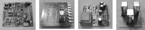
Table lists the components (both valuable and toxic ones) to be extracted from the selected boards.
Table 1 Components to be recycled.
The alternatives for the reuse of these components have been analysed, and the best option is to integrate them into the main production flow of the same electronic boards. The extracted components will be tested before being reused, by means of the same testing machines used in the assembly line.
Once the components to be reused are defined, identification methods must be evaluated (automated, semi-automated or manual). The aim is to inform the disassembling system about their location and orientation in the PCB, and the best way to desolder and handle them. In this case, the selected components are already known, and, in order for the proposed recycling system to be economically feasible for the final user, some technical steps have been simplified, applying basic technical solutions. One of these is the method to identify the type of board to be processed by the system. The worker will give this information by means of a switching device. More complex or automated solutions (based on the component or board identification using machine vision) have been discarded owing to their cost or the specific requirements and constraints of the workforce.
The proposed identification system is composed of the following elements:
| • | Output screen, with two functions. During the system programming phase, it will be used to configure desoldering and handling operations. On regular function phase, it will display different PCB models, so that the user can select one of them. | ||||
| • | Alphanumeric keyboard, to allow control of the system for configuration and working procedures. | ||||
| • | Programmable logic controller (PLC) to control the automated operations, and auxiliary electric and electronic equipment. | ||||
3. Simulation
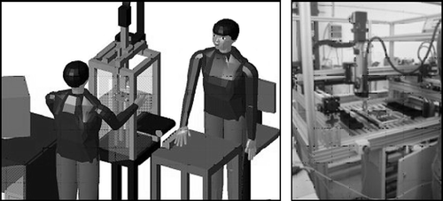
In this step, simulation and optimisation of the disassembly phases are carried out. A virtual prototype is created, composed of 3D models of PCBs, components and disassembly devices (Figure ). Their operation is analysed by means of simulation technology, with the aim of evaluating different options of plant layout. In addition, technical details regarding specific features of desoldering and handling operations are simulated. As a result, an optimised disassembly sequence is obtained, taking into account all the technical constraints.
Figure 2 Modelling of PCBs and handling device.
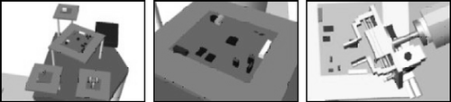
At laboratory level, a six-axis robot has been used to extract and handle the components from the PCBs. A specifically designed gripper with two types of fingers has been developed, with the aim of handling all the envisaged components with that only gripper (Figure ).
Figure 3 Simulated (left) and real robotised cell (centre and right).
As a result of the simulation studies, technical features of the handling system were defined:
| • | Payload: able to handle the different disassembling tools. | ||||
| • | It should be able to interface with other equipments. | ||||
| • | Linear and angular movements in 3D to allow a precise positioning. | ||||
| • | Positioning precision of 0.5 mm, trajectory precision is not so important. | ||||
| • | Position repeatability under 0.5 mm. | ||||
| • | Working volume: it must allow the access to all components in the PCB. A minimum of 250 × 250 mm to reach the PCBs, plus the required distance to reach the stores for the extracted components. | ||||
| • | Programming capabilities able to manage different logic control for each type of PCB. | ||||
| • | The system should be able to work in the temperature range in which the desoldering equipment works. | ||||
4. Desoldering of components
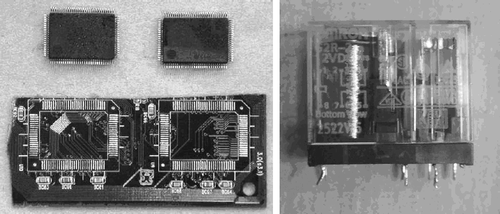
Three methods have been tested in order to achieve a non-destructive desoldering of joints between components and surface of the PCBs. These processes have been applied to two types of assembly technologies: ‘thru-hole’ (component's pins go thru the board) and ‘surface mounted devices’, SMD, where the pins are joined only to the upper part of the board (Figure ).
Figure 4 Desoldered SMD components (left) and thru-hole components (right).
4.1 Desoldering by melting in vapour phase
This method has been applied to SMD components, using the heat generated by the vapour phase of an inert liquid, a common technology applied in the electronic industry to solder components. Heat causes the soldered joints to melt. Results showed that there is no damage in the components or PCBs, but this option has been rejected owing to the time needed (about 40 min) to achieve the required temperature (215°C) and the specific requirements of the solution.
4.2 Desoldering by heating using infrared radiation
This method can be applied to both SMD and thru-hole components. The infrared radiation has been focused on the side of the PCB containing the soldered joints in the case of thru-hole elements. In order to minimise the risk of damage to the components, several parameters must be carefully controlled:
| • | transmitted power; | ||||
| • | type of infrared lamps; | ||||
| • | distance between transmitter and PCB; and | ||||
| • | exposure time. | ||||
Several drawbacks have been detected: the radiation may cause damage to the layers of the PCBs (depending on their composition), and also to the electronic part of the SMD components (covered by the packaging), since the temperature is about 220°C during 150 s. This solution demands a fine tuning of the above mentioned parameters, and consequently makes the final system more complex and expensive.
4.3 Desoldering by heating using hot air jet
This technology used to be applied to SMD components, but it also works properly with thru-hole elements. The equipment is a commercial soldering/desoldering station (JBC AM 6500), composed of a hot air generator, diffusing head and vacuum grippers to extract the desoldered component. The process consists of the positioning of the vacuum gripper over the components, application of a heated air jet over the soldered joints and extraction of the released component. Similar parameter control as with infrared method must be taken:
| • | air flow and temperature; | ||||
| • | exposure time; and | ||||
| • | distribution of air over the connection pins. | ||||
As a result from the performed tests, the following conclusions have been obtained:
| • | no damage has been done to the electronic part of the components owing to the short exposure time; | ||||
| • | desoldering times are shorter than the ones obtained using the infrared method; | ||||
| • | an important issue here is the right diffusion of the hot air over the connection pins which must be homogeneous and focused on the soldered pins, avoiding the packaging part of the SMD component; and | ||||
| • | it is necessary to design a specific head for the desoldering and disassembly functions. | ||||
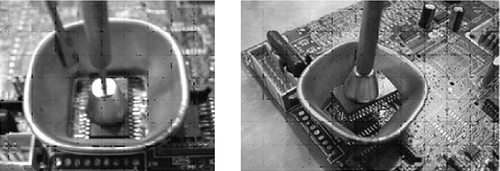
Figure shows the process of desoldering and extracting a SMD component.
Figure 5 Application of heat (left) and component extraction (right).
When dealing with thru-hole components, a similar solution can be applied. The hot air is focused on the side of the PCB where the soldered pins are located, so there is no risk of damage to the electronic parts. In this case, the gripper is equipped with two finger tweezers, since the vacuum solution cannot be used owing to the geometry of the components. Table shows the final results concerning the temperature and time needed to desolder the components.
Table 2 Components and required desoldering temperatures and times.
5. Handling system at industrial level
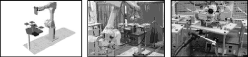
Since the tasks for the extraction of the components do not require complex movements and orientation of the manipulator and gripper, the robot used in the laboratory is no longer needed. In order to extract, handle and classify the components in separated stores, a more simple automatic handling system is proposed. The manipulator should be composed of three linear axes which perform controlled movements X, Y and Z to pre-programmed positions. A positioning accuracy of 0.5 mm is required, together with a working area of at least 250 × 250 mm. As a first step, a 3D model of the overall system has been used in order to simulate the function of the automatic system (Figure ).
Figure 6 Simulation of the proposed system, and real manipulator.
The SMD components (memories and microprocessors) will be extracted from the PCB using a vacuum gripper. Thru-hole components, on the other side, will be handled by means of a two finger pneumatic gripper (Figure ). A specific handling tool has been designed with the following features:
| • | interchangeable adaptor to fit the tools to different grippers (vacuum and tweezers);
Figure 7 Pneumatic gripper and vacuum gripper located in the manipulator. 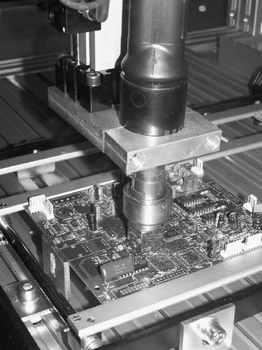 | ||||
| • | compact system that includes pneumatic actuators, control valves and vacuum generator; | ||||
| • | it is a modular system, allowing changes in the required gripper in an autonomous way; | ||||
| • | Venturi effect to create vacuum, using silent ejectors; and | ||||
| • | pneumatic tweezers with interchangeable fingers and controlled open/close operation. | ||||
Previous simulation of the manipulating system has allowed the analysis of different parameters, such as working area of the manipulator and gripper, and collision detection between gripper, PCBs and fixing system of the station.
The control of the trajectories to perform the disassembly tasks is done by a PLC. A specific program for each type of PCB is recorded, containing the positions of every component within the PCB, and the final destination of the recovered elements to a specific storage area. The program also contains the desoldering parameters (temperature, time, etc.) required by each component.
The desoldering system works with a temperature range of 150–455°C, with an air flow between 6 and 45 l/min. It includes a specifically designed head to focus the air jet on the area of interest.
Finally, the PCBs are fixed in a table by means of a flexible frame, able to be adapted to the different sizes and geometry of PCBs to be treated. It is made of aluminium to reduce the weight. This material is also useful to disperse the heat.
The system was set up in the facilities of the company Lantegi Batuak, where it was tuned to the real conditions of the PCBs received from production rejection. The company also expects to receive, in the near future, disposed end-of-life appliances containing those specific PCBs, in order to be processed in the proposed system. The economic data resulting from the first tests of the system give the following results (Table ).
Table 3 Economic data obtained from the proposed system.
The first conclusion from the data shown above is the fact that the recycling system is feasible, from the economic point of view, only if the number of PCBs to be treated is high. That means that the main goal of the proposed system should be to recycle disposed end-of-life electric appliances and not only the treatment of the PCBs coming from production rejection (5% annually). From the environmental perspective, this solution guarantees a proper handling of the toxic components obtained from the boards.
6. Summary
The main objective of this work has been the definition of a simulation-based methodology for a selective and non-destructive disassembly of electronic components in PCBs, coming from production rejections, aimed at their reuse in similar or new applications, and with a feasible cost for the user. A disassembly and handling station has been developed, based on a hot air jet system to desolder the components, and a three axes manipulator with vacuum and gripping systems to extract and handle the recovered elements. They will be used again in the manufacturing of PCBs of the same type. In addition, toxic components are also extracted and conveniently managed, thus avoiding the disposal of hazardous substances to the environment.
The main innovations are the solutions applied to the desoldering and handling of the components, as they are simple and at low costs: the tasks are semi-automatic, most of them are based on manual procedures, with a basic mechanical design of the equipment.
Acknowledgements
This project has been developed together with Gaiker Technology Centre, and has been partially funded by the Spanish Ministry of Industry. We would also like to thank Fundacion Lantegi Batuak for its technical support and advice. The final system is currently working in its premises.
References
- Brandstötter, M., Knoth, R., Kopacek, B. and Kopacek, P., 2003. Cheklist for optimized design for re-use of printed wire boards and components. Proceedings of the IEEE international symposium on electronics and the environment, 19–22 May 2003, Boston. 165–168
- Dembowski, H., Pötter, H., Polityko, D., Schrank, K. and Stobbe, I., 2000. Automated disassembly of PCBs for reuse and quality control of desoldered packages. Joint international congress goes green 2000+, 11–13 September 2000, Berlin
- Eswaraiah , C. , Cavita , T. , Vidyasagar , S. and Narayanan , S.S. 2008 . Classification of metals and plastics from printed circuit boards (PCB) using air classifier . Chemical Engineering and Processing: Process Intensification , 47 ( 4 ) : 565 – 576 .
- Goosey, M. and Kellner, R., 2002. A scoping study: end-of-life printed circuit boards [online]. Surrey, Center for Sustainable Design. Available from: http://www.cfsd.org.uk/seeba/TD/reports/PCB_Study.pdf [Accessed 18 October 2008)
- Hall , W.J. and Williams , P.T. 2007 . Separation and recovery of materials from scrap printed circuit boards . Resources, Conservation and Recycling , 51 ( 3 ) : 691 – 709 .
- Jacob, P., Schürch, S. and Holberg, T., 1998. Re-use of integrated circuits (ICs) as an added-value in recycling of electronic waste. Proceedings of CARE innovation conference, 16–19 November 1998, Vienna
- Martin , I. 2006 . Europe en route to a recycling society . Recycling International , : 38 – 43 .
- Moua , P. , Xianga , D. and Duan , G. 2007 . Products made from nonmetallic materials reclaimed from waste printed circuit boards . Tsinghua Science and Technology , 12 ( 3 ) : 276 – 283 .
- Pötter, H., Griese, H., Middendorf, A. and Fotheringham, G., 1998. Quality insurance for the re-use of electronics estimating the remaining life by optical interconnect examination. Proceedings of CARE innovation conference, 16–19 November 1998, Vienna. 288–294
- Pötter, H., Griese, H., Middendorf, A., Fotheringham, G. and Reichl, H., 1999. Towards the re-use of electronic products – quality assurance for the re-use of electronics. International symposium on environmentally conscious design and inverse manufacturing: eco-design '99, 1–3 February 1999, Tokyo. 288–292
- Renteria, A., Alvarez, E. and López, J.M., 2007a. A review of automation alternatives for recycling plants of electronic appliances. Proceedings of 17th FAIM conference, 30 June–2 July 2007, Philadelfia. 996–1003
- Renteria, A., Alvarez, E. and Pérez, J., 2007b. Proposal of a semi-automated demanufacturing plant for electronic waste. Proceedings of 24th international manufacturing conference, 29 July–1 August 2007, Waterford. 373–379
- Sen, H., 2007. Method of recycling waste printed circuit boards, European Patent N. EP1811821
- Stobbe, I., Griese, H., Pötter, H., Fotheringham, G. and Reichl, H., 2004. Quality challenges of reuse components. Proceedings of Asian green electronics conference, 5–6 January 2004, Hong Kong. 218–225
- Urch, Ph., Kopacek, B. and Kopacek, P., 2002. A modular control concept for disassembly cells. Proceedings of CARE 2002, 25–28 November 2002, Vienna
- Van den Herten, K., 2007. Directive 2002/96/EC of the European Parliament and of the Council on waste electrical and electronic equipment (WEEE). Proceedings 6th international recycling congress, 18–20 January 2007, Hamburg
- Yoo , J.M. , Jeong , J. , Yoo , K. , Lee , J. and Kim , W. 2009 . Enrichment of the metallic components from waste printed circuit boards by a mechanical separation process using a stamp mill . Waste Management , 29 ( 3 ) : 1132 – 1137 .
- Zhenga , Y. , Shen , Z. , Caia , C. , Maa , S. and Xinga , Y. 2009 . The reuse of nonmetals recycled from waste printed circuit boards as reinforcing fillers in the polypropylene composites . Journal of Hazardous Materials , 163 ( 2 ) : 600 – 606 .
