Abstract
Zinc oxide (ZnO) thin film as a piezoelectric material for microelectromechanical system (MEMS) actuators and sensors was evaluated. ZnO thin films were deposited using radio frequency (RF) magnetron sputtering. Process parameters such as gas ratio, working pressure, and RF power were optimized for crystalline structure. The ZnO thin films were characterized by X-ray diffraction (XRD) and scanning electron microscopy (SEM). Good quality of ZnO thin films was further confirmed by a high transverse piezoelectric coefficient d 31. A microcantilever was then designed, fabricated, and characterized. Design formulas of resonant frequency, actuation, and sensing sensitivities were derived. The resonant frequency was determined by an impedance analyzer. Tip deflection on nanometer level was demonstrated with the cantilever used as an actuator. The actuation sensitivity was found to be 12.2 nm/V. As a sensor, the cantilever was calibrated against a reference accelerometer. The sensing sensitivity was characterized to be 46 mV/g. The characterization results were compared with design specifications. The differences were caused mainly by thickness control in etching. This study showed that ZnO is a promising piezoelectric material for MEMS actuators and sensors in terms of excellent process compatibility and good piezoelectric performance.
Keywords:
1. Introduction
Piezoelectric cantilevers can be used as actuators or sensors. As actuators, they utilize the converse piezoelectric effect to convert electrical energy into mechanical energy, i.e. displacement and force. As sensors, they operate in the opposite mode using the piezoelectric effect. Typical piezoelectric cantilever actuators include ultrasonic motors Citation[1], atomic force microscopy (AFM) probes Citation[2], microelectromechanical system (MEMS) switches Citation[3,Citation4], bandpass filters Citation[5], and scanning MEMS mirrors Citation[6,Citation7], whereas piezoelectric cantilever sensors can be accelerometers, force sensors, or pressure sensors [Citation8–10 Citation Citation10].
Among the broad range of piezoelectric materials, lead zirconate titanate (PZT) is most widely used due to its superior piezoelectricity. Piezoelectric devices can be made of bulk or thin-film PZT. A wide variety of sensors and actuators based on bulk PZT are successfully manufactured using conventional technologies. Compared with its success in conventional transducers, applications of PZT in MEMS are rather limited due to integration issues of PZT thin films Citation[11]. Preparation of PZT usually involves high temperatures above 500°C Citation[12,Citation13]. High-temperature processing can cause interfacial structural failures and changes in dopant profiles of electrical elements in integrated circuits Citation[14].
Apart from PZT, zinc oxide (ZnO) is another important piezoelectric material. Piezoelectricity of ZnO is generally one order smaller than that of PZT Citation[15]. The biggest advantage of ZnO over PZT is its greater flexibility in processing. ZnO thin films can be deposited using radio frequency (RF) magnetron sputtering, chemical vapor deposition, molecular beam epitaxy, pulsed laser deposition, etc. Citation[16]. RF magnetron sputtering is one of the most popular growth techniques due to its low cost, low operating temperature, good reproducibility, and compatibility with surface micromachining technologies. In addition to flexibility in deposition, ZnO thin films can be easily etched by a variety of acidic etchants Citation[17]. Therefore, it can be readily integrated with other MEMS materials and processes.
Due to its good piezoelectricity and processing compatibility, ZnO has been successfully used in thin-film piezoelectric devices such as surface acoustic wave (SAW) devices and MEMS transducers. SAW devices typically consist of a transmitter and a receiver. The transmitter converts electrical signals into mechanical waves which propagate to the receiver. Since velocity of acoustic waves changes with surface conditions, gas or mass concentrations on the surface can be measured by the frequency shift. SAW devices are especially useful as chemical sensors and biosensors Citation[18]. SAW sensors based on ZnO thin film or nanorods with different substrate have been demonstrated for NO2 and H2 gas sensing Citation[19,Citation20]. The performance of a SAW device depends mainly on the acoustic velocity and the electromechanical coupling coefficient. To calculate the sensitivity of SAW devices, a technique based on a Green's function has been proposed Citation[21]. It was found that the ZnO/LiTaO3 devices had high mass sensitivity and electromechanical coupling, which is advantageous for sensing changes in the conductivity of the selective layer.
Cantilever-type sensors and actuators are the most common among ZnO-based piezoelectric MEMS transducers. Low-frequency micromechanical cantilever actuators using ZnO thin film was earlier modeled as a metal–oxide–semiconductor (MOS) structure Citation[22]. An approximate formula for tip deflection was proposed based on the MOS structure. This modeling approach did not address piezoelectric actuators as electromechanical devices. In later theoretical works, piezoelectric cantilevers were modeled based on the constitutive equations of piezoelectric materials, internal energy, and force and moment equilibrium conditions. The tip deflection and electrical charge of piezoelectric bimorphs were obtained by calculation of internal energy and canonical conjugates of applied force, moment, and voltage Citation[23,Citation24]. Constitutive equations for multilayer piezoelectric cantilevers with a more general configuration were derived from equilibrium conditions and beam curvature Citation[25,Citation26]. In the aforementioned studies, the electric field across the piezoelectric layer was conveniently assumed constant due to the small thickness of the thin-film piezoelectric layer. A more recent effort presented closed-form relationships for multilayer piezoelectric cantilever beams without assuming small piezoelectric coupling Citation[27]. In addition, a new characterization technique using the beam curvature to identify the transverse piezoelectric coefficient d 31 was introduced in that study.
Among various applications of ZnO-driven cantilevers, AFM scanning probes have been receiving the most interest. ZnO-driven cantilevers were used to enhance the scanning speed of the AFM Citation[28,Citation29]. The studies were focused on the performance of the imaging bandwidth of the AFM. ZnO thin film preparation and the characteristics of the ZnO actuator were not reported. In a similar work, the traditional piezotube actuator in an AFM was replaced by an integrated piezoelectric ZnO cantilever Citation[30]. As a result, the speed of the tapping mode was improved by over an order of magnitude. Moreover, a piezoelectric cantilever with a sputtered ZnO thin film as a sensor and actuator was applied on the AFM Citation[31]. Although the transverse piezoelectric coefficient was characterized, its value was low due to the suboptimal sputtering process. The resonant frequency was estimated using a simplified formula and not experimentally determined. The actuation and sensing sensitivities of the cantilever were not characterized either. In addition to use of ZnO microcantilevers to enhance imaging speed of the AFM, ZnO nanocantilevers have been exploited to increase force sensitivity of the scanning probe. ZnO nanocantilevers fabricated from nanobelts were demonstrated on an AFM probe Citation[32]. With dimensions several orders of magnitude smaller than conventional cantilevers, the ZnO nanocantilevers were expected to have ultrahigh sensitivity to tip-surface interactions.
This article presents a comprehensive study on ZnO thin film preparation, characterization, and its actuation and sensing performances. ZnO thin films were deposited using RF magnetron sputtering. The sputtering conditions for ZnO were optimized to achieve best crystalline structure which leads to a high transverse piezoelectric constant d 31. A microcantilever was fabricated to evaluate the piezoelectric properties of the ZnO thin film. Its resonant frequency, actuation and sensing sensitivities were characterized and compared with theoretical values.
2. Preparation of ZnO thin films
The quality of sputtered ZnO thin films (crystalline orientation, surface roughness, grain size, etc.) is dependent on sputtering parameters such as bias power, gas pressure, gas ratio of O2/Ar, and temperature Citation[18]. In this study, the effects of the sputtering parameters have been investigated using X-ray diffraction (XRD) and scanning electron microscopy (SEM).
2.1. Sputtering parameters
ZnO with 99.99% purity, 50 mm in diameter, and 3 mm in thickness was used as a target in the RF magnetron sputtering system. The substrate was a 4-inch diameter p-type silicon (100) wafer. Before the deposition process, the silicon wafer went through a thermal oxidation process, whereby SiO2 of 1-μm-thick was grown on top of the wafer. Au/Ti with thickness of 300 nm/50 nm was then deposited onto the wafer before the deposition of ZnO. The Ti layer was used to increase the adhesion between the Au and SiO2 layers.
Upon placing both the target and substrate inside the chamber of the RF magnetron sputtering machine, the pressure inside the chamber was pumped down to around 10 Pa before it was further pumped down to 6 × 10⁻⁴ Pa using a molecular pump. shows the operating parameters used for the deposition of ZnO thin films. Three parameters were varied in order to find the best operating parameters which can produce the best crystalline structure of ZnO. They were RF power, working pressure, and gas ratio.
Table 1. Deposition parameters of ZnO thin film
2.2. Characterization of ZnO thin films
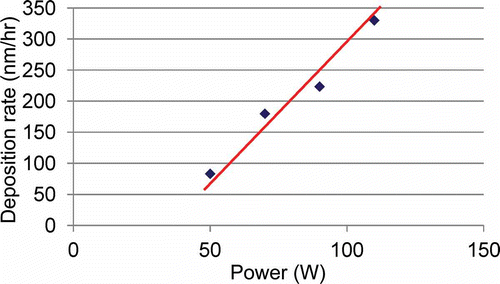
The cross section of the ZnO thin film was observed by field-emission SEM (FE-SEM; JEOL JSM-7600F; JEOL Ltd., Tokyo, Japan). The ZnO crystalline structure was characterized and analyzed by XRD (Philips PW 1830; Philips Analytical Inc., Natick, MA, USA). The deposition rate with respect to different power of the RF magnetron sputtering system was first studied. The thickness of the ZnO thin film was measured with FE-SEM, and it was then divided by deposition time (2 hr in the experiment) to yield the deposition rate in nm/hr. shows the deposition rate with respect to different power. It can be seen that the deposition rate of the ZnO thin film has a linear relationship with the RF power. With higher RF power, a thicker ZnO thin film could be achieved in the same period of time. However, it is not advisable to use too high power as it would cause the ZnO polycrystalline structure to be randomized within the thin film. This would greatly affect the piezoelectric behavior of the ZnO thin film.
Figure 1. Deposition rate of ZnO thin film with respect to the RF power in the magnetron sputtering system.
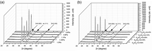
The ZnO crystalline structure under different working pressure and gas ratio was then analyzed with XRD. shows the XRD pattern for the two different parameters. Under different working pressure, it can be seen in (a) that the maximum intensities of each working pressure all fall at around 34° of diffraction angle for the 2θ (degree). It shows that all ZnO thin films have a preferred c -axis orientation. However, it can be further noticed that at the working pressure of 0.8 Pa, the intensity peak is the highest among the rest. This shows that at 0.8 Pa, the ZnO thin film has a very good crystalline quality and has a better orientation compared to those deposited at other working pressure. Under different gas ratios ((b)), it was once again proven that the ZnO thin film has a preferred c -axis orientation as all intensity peaks fall at around 34° of diffraction angle too. And at the gas ratio of 50% (equal amount of oxygen and argon gas), the intensity peak is the highest which implies that at 50% gas ratio, the deposited ZnO thin film has the best crystalline quality. shows the cross section of a typical ZnO thin film. It further proves that the deposited ZnO thin film has a preferred c -axis orientation since the ZnO crystalline structure has a vertical columnar structure.
Figure 3. SEM image of the cross-sectional ZnO thin film.
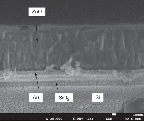
Figure 2. XRD patterns of ZnO thin film under: (a) various working pressure and (b) various gas ratios.
3. Cantilever design
Resonant frequency and sensitivity are the most important specifications for actuators and sensors. The resonant frequency together with damping determines the bandwidth of a transducer. In addition, the sensitivity is directly related to the signal-to-noise ratio of the output. Ideally, both parameters are preferred to be as big as possible; however, a trade-off exists between them. It usually depends on the application requirements to determine an appropriate combination.
3.1. Resonant frequency
The fundamental resonant frequency, fn , of a beam clamped at one end and free at the other end is given by Citation[33]
where E, I, m, and L are the Young's modulus, area moment of inertia, mass per unit length, and length of the beam, respectively. To find the flexural rigidity EI for the piezoelectric cantilever which consists of two materials, the transformed-section method is used to transform its cross section into an equivalent cross section of a single material Citation[34]. Thus, the resonant frequency fn becomes
where the subscripts p and s denote piezoelectric and elastic materials, respectively; and ρ and t are the density and thickness, respectively.
3.2. Actuation and sensing sensitivities
Actuation sensitivity of a cantilever actuator is typically defined by the ratio of tip deflection δ to driving voltage V. The actuation sensitivity of a heterogeneous piezoelectric bimorph is given by Citation[23,Citation25]
A piezoelectric cantilever as a sensor can be used to measure acceleration. The charge Q induced by an acceleration field a is Citation[23]
where w is the width of the cantilever, while the capacitance of a heterogeneous piezoelectric bimorph C is Citation[23]
where is the permittivity at constant stress. The open-circuit output voltage V = Q/C. With acceleration as the input, the sensor sensitivity therefore is
3.3. Design specifications
The resonant frequency of the piezoelectric cantilever is used as the primary design parameter. After setting a target resonant frequency, the thickness of the piezoelectric layer can be determined. Subsequently, the actuation and sensing sensitivities can be calculated. The full design specifications are shown in .
Table 2. Design specifications of the ZnO piezoelectric cantilever
4. Fabrication of cantilever
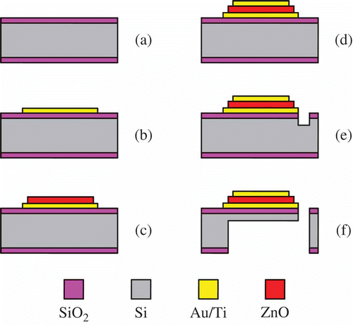
The cantilever was fabricated on a p-type (100) silicon wafer by microfabrication. The fabrication process flow is shown in . The fabrication process started with oxidation of the silicon wafer ((a)). The oxide layer provides insulation between the bottom electrode and the silicon substrate. Au/Ti of 100-nm-thick was first deposited for the bottom electrode ((b)). A ZnO layer of 1-μm-thick was then sputtered at room temperature ((c)), followed by deposition of the top electrode, another 100 nm of Au/Ti ((d)). After deposition of the thin films, the wafer underwent deep reactive ion etching to carve out the mechanical structure. This was done in two steps. First, the cantilever pattern was defined by etching from the front side ((e)). Second, a cavity was cut from the back side to free the cantilever ((f)). The thickness of the silicon beam was controlled by etching time. A total of five photo-masks were used for the fabrication. The fabricated ZnO cantilever is shown in
Figure 5. Fabricated ZnO cantilever.
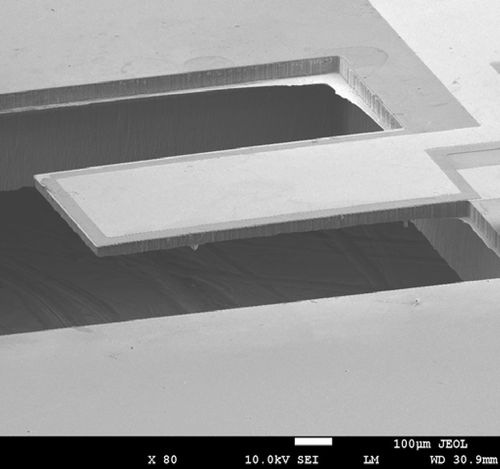
Figure 4. Fabrication process flow: (a) oxidation, (b) Au/Ti deposition, (c) ZnO deposition, (d) Au/Ti deposition, (e) front-side etching, and (f) back-side etching.
5. Characterization of cantilever
The resonant frequency of the cantilever and its actuation and sensing activities were characterized and compared with the design specifications. The transverse piezoelectric coefficient d 31 was also calculated using measured tip deflection and driving voltage.
5.1. Resonant frequency
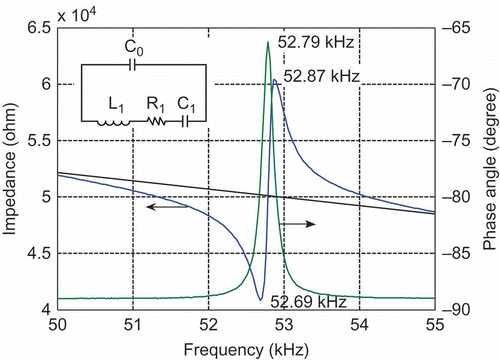
A piezoelectric vibrator can be represented by a lumped-parameter equivalent circuit near an isolated resonance [35]. Thus, the resonant frequency of the fundamental mode of the cantilever can be found by measuring its impedance properties. shows the measured resonant frequency of the ZnO cantilever using an impedance analyzer (Agilent 4294A; Agilent Technologies Inc., Santa Clara, CA, USA). The resonance appears at 52.87 kHz, which is 6% higher than the design specification (). This is mainly caused by the difference between the actual thickness and the design value. There are two major reasons for this discrepancy. First, the metal electrodes were not considered in modeling, which add to the total thickness, thus increase the resonant frequency. Second, the thickness was controlled by etching rate which usually has poor accuracy; as a result, the silicon layer may be significantly thicker than that in the design.
Figure 6. Impedance and phase angle.
5.2. Actuator and sensor sensitivities
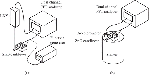
Vibration testing was performed to find the actuation and sensing sensitivities of the piezoelectric cantilever. The experimental setup is shown in . For actuator characterization, as shown in (a), the cantilever was driven by voltage supplied by a function generator (Agilent 33120A). Tip deflection of the cantilever was captured by a laser Doppler vibrometer (Polytec Inc. Irvine, CA, USA). Signals of the driving voltage and tip deflection were processed by a dual channel fast Fourier transform (FFT) spectrum analyzer (ONO SOKKI CF-5220Z; ONO SOKKI Co., Yokohama, Japan). The actuator sensitivity can be calculated by dividing the tip deflection (output) by the driving voltage (input). As shown in (b), the cantilever was excited by a shaker (B&K 4810; Brüel & Kjær Sound and Vibration Measurement A/S, Næum, Denmark) for sensor characterization. Acceleration of the shaker was measured by a reference accelerometer (B&K 4374). The acceleration signal was used as the input in conjunction with the output voltage of the cantilever to calculate the sensor sensitivity.
Figure 7. Characterization setup: (a) actuator characterization and (b) sensor characterization.
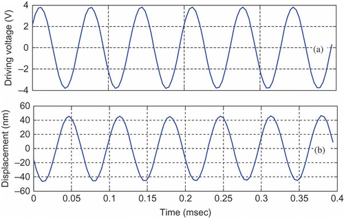
Plotted in are time histories of driving voltage at 15 kHz and the resultant tip deflection. The amplitudes of the driving voltage and tip deflection are 3.8 V and 46 nm, respectively. The actuation sensitivity for this case is 12.1 nm/V. The tip deflection lags 0.035 msec behind the driving voltage, which corresponds to a phase lag of 190°.
Figure 8. Actuator response at 15 kHz: (a) driving voltage and (b) tip deflection.
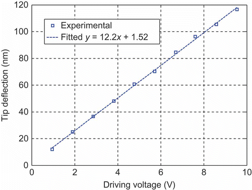
To investigate the linearity of the tip deflection in response to increasing driving voltage, the cantilever was tested for driving voltage ranging from about 1 V to almost 10 V. The amplitude of the tip deflection is plotted against that of the voltage in . The fitted line shows that the sensitivity is 12.2 nm/V with good linearity. Compared with the design specification (13.5 nm/V), the experimental sensitivity is 9.6% lower. This is due to the same reasons behind the higher measured resonant frequency.
Figure 9. Tip deflection versus driving voltage.
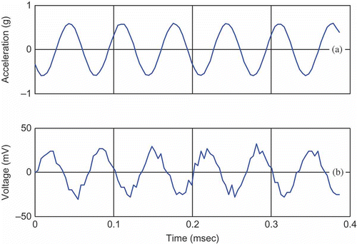
The piezoelectric effect of the ZnO thin film was evaluated by base excitation supplied by a shaker (B&K 4810). The output voltage of the ZnO cantilever was benchmarked against that of a commercial accelerometer (B&K 4374). Time histories of the base acceleration and the output voltage of the cantilever at 15 kHz are shown in . Similar to the actuator output, the sensor also lags behind the input. The sensor lag (0.043 msec) is slightly longer than the actuator lag (0.035 msec). Comparing (b) and (b), it can be seen that the response of the actuator is smoother than the sensor. The amplitudes of the acceleration and sensor output are 0.59 g and 26.56 mV, respectively. This corresponds to a sensitivity of 45 mV/g. The amplitude of the sensor output increases with the base excitation (). The fitted sensitivity is 46 mV/g. For the same reasons as explained for the resonant frequency and actuation sensitivity, the sensing sensitivity is 14% lower than the design specification (53.6 mV/g). Nonlinearity of the sensor, defined as the ratio of maximum output deviation to full scale output Citation[36], was found to be 8.8% full scale (FS).
Figure 11. Cantilever output voltage versus base acceleration.
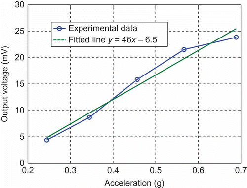
Figure 10. Sensor response at 15 kHz: (a) acceleration and (b) output voltage.
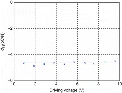
5.3. Transverse piezoelectric coefficient d31
The transverse piezoelectric coefficient d
31 can be found using the measured tip deflection and driving voltage. According to EquationEquation (3)(3), the transverse piezoelectric coefficient d
31 is
Using the driving voltage and corresponding tip deflection shown in , the calculated d 31 is plotted against the driving voltage in . Its absolute average value is 4.66 pC/N, which is lower than that of bulk ZnO (5.2 pC/N) Citation[15].
Figure 12. Calculated d 31 versus driving voltage.
6. Conclusions
This article presents design, fabrication, and characterization of a piezoelectric ZnO cantilever for actuation and sensing applications in MEMS transducers. ZnO thin films have been deposited using RF magnetron sputtering under room temperature. Characterization results with SEM and XRD showed highly c -axis-oriented ZnO crystals.
A microcantilever was designed and fabricated to demonstrate applications of ZnO thin films in nanoscale actuation and sensing. The actuation and sensing performances of the fabricated piezoelectric cantilever were characterized and compared with design specifications. The resonant frequency measured by an impedance analyzer was 53 kHz, 6% higher than the design value. This was believed to have been caused by inaccurate thickness control during etching and omission of metal electrodes in modeling. Due to the trade-off between resonant frequency and sensitivity, both the actuation and sensing sensitivities were found lower than the design specifications. The actuation sensitivity was characterized to be 12.2 nm/V, 9.6% lower than the design value (13.5 nm/V), while the sensing sensitivity was 46 mV/g, 14% lower than the design value (53.6 mV/g). The cantilever showed better linearity in actuation than sensing.
This study shows ZnO thin film as a piezoelectric material possesses significant advantages over PZT in MEMS applications. Its low-temperature deposition process allows it to integrate with other MEMS materials without causing structural failures such as crack. Although PZT is superior to ZnO in terms of piezoelectricity, ZnO thin films demonstrated actuation and sensing performances which are adequate for micro and nano applications. In advanced MEMS systems, in which process integration is a major concern, ZnO can be a better choice than PZT.
References
- Morita , T. 2003 . Miniature piezoelectric motors . Sensor. Actuator: Phys , 103 : 291 – 300 .
- Miyahara , Y. , Deschler , M. , Fujii , T. , Watanabe , S. and Bleuler , H. 2002 . Non-contact atomic force microscope with a PZT cantilever used for deflection sensing, direct oscillation and feedback actuation . Appl. Surf. Sci , 188 : 450 – 455 .
- Kugeler , C. , Hennings , A. , Bottger , U. and Waser , R. 2009 . An integrated microelectromechanical microwave switch based on piezoelectric actuation . J. Electroceram , 22 : 145 – 149 .
- Sinha , N. , Jones , T.S. , Guo , Z.J. and Piazza , G. 2012 . Body-biased complementary logic implemented using AlN piezoelectric MEMS Switches . J. Microelectromech. Syst , 21 : 484 – 496 .
- Tu , W.H. and Chang , K. 2007 . Piezoelectric transducer-controlled dual-mode switchable bandpass filter . IEEE Microw. Wireless Compon. Lett , 17 : 199 – 201 .
- Koh , K.H. , Kobayashi , T. and Lee , C. 2011 . A 2-D MEMS scanning mirror based on dynamic mixed mode excitation of a piezoelectric PZT thin film S-shaped actuator . Optic Express , 19 : 13812 – 13824 .
- Koh , K.H. , Kobayashi , T. , Hsiao , F.L. and Lee , C. 2010 . Characterization of piezoelectric PZT beam actuators for driving 2D scanning micromirrors . Sensor. Actuator: Phys , 162 : 336 – 347 .
- Zou , Q. , Tan , W. , Kim , E.S. and Loeb , G.E. 2008 . Single-and triaxis piezoelectric-bimorph accelerometers . J. Microelectromech. Syst , 17 : 45 – 57 .
- Lee , C.K. , Itoh , T. and Suga , T. 1996 . Micromachined piezoelectric force sensors based on PZT thin films . IEEE Trans. Ultrason. Ferroelectrics Freq. Contr , 43 : 553 – 559 .
- Mortet , V. , Petersen , R. , Haenen , K. and ’Olieslaeger , M. D . 2006 . Wide range pressure sensor based on a piezoelectric bimorph microcantilever . Appl Phys Lett , 88 : 133511–1 – 133511–3 .
- Trolier-McKinstry , S. and Muralt , P. 2004 . Thin film piezoelectrics for MEMS . J. Electroceram , 12 : 7 – 17 .
- Jaffe , B. , Cook , W.R. and Jaffe , H.L. 1971 . Piezoelectric Ceramics , New York : Academic Press .
- Kobayashi , T. , Ichiki , M. , Tsaur , J. and Maeda , R. 2005 . Effect of multi-coating process on the orientation and microstructure of lead zirconate titanate (PZT) thin films derived by chemical solution deposition . Thin Solid Films , 489 : 74 – 78 .
- Polla , D.L. and Francis , L.F. 1998 . Processing and characterization of piezoelectric materials and integration into microelectromechanical systems . Annu. Rev. Mater. Sci , 28 : 563 – 597 .
- Ikeda , T. 1990 . Fundamentals of Piezoelectricity , Oxford : Oxford University Press .
- Ozgur , U. , Alivov , Y.I. , Liu , C. , Teke , A. , Reshchikov , M.A. , Dogan , S. , Avrutin , V. , Cho , S.J. and Morkoc , H. 2005 . A comprehensive review of ZnO materials and devices . J. Appl. Phys , 98 : 041301–1 – 041301–103 .
- Xu , T. , Wu , G.Y. , Zhang , G.B. and Hao , Y.L. 2003 . The compatibility of ZnO piezoelectric film with micromachining process . Sensor. Actuator: Phys , 104 : 61 – 67 .
- Fu , Y.Q. , Luo , J.K. , Du , X.Y. , Flewitt , A.J. , Li , Y. , Markx , G.H. , Walton , A.J. and Milne , W.I. 2010 . Recent developments on ZnO films for acoustic wave based bio-sensing and microfluidic applications: A review . Sensor. Actuator: Chem , 143 : 606 – 619 .
- Ippolito , S.J. , Kandasamy , S. , Kalantar-zadeh , K. , Wlodarski , W. , Galatsis , K. , Kiriakidis , G. , Katsarakis , N. and Suchea , M. 2005 . Highly sensitive layered ZnO/LiNbO3 SAW device with InOx selective layer for NO2 and H2 gas sensing, Sensor. Actuator: Chem , 111–112 : 207 – 212 .
- Sadek , A.Z. , Wlodarski , W. , Li , Y.X. , Yu , W. , Li , X. , Yu , X. and Kalantar-zadeh , K. 2007 . A ZnO nanorod based layered ZnO/64° YX LiNbO3 SAW hydrogen gas sensor . Thin Solid Films , 515 : 8705 – 8708 .
- Powell , D.A. , Kalantar-zadeh , K. and Wlodarski , W. 2004 . Numerical calculation of SAW sensitivity: Application to ZnO/LiTaO3 transducers . Sensor. Actuator: Phys , 115 : 456 – 461 .
- Blom , F.R. , Yntema , D.J. , Vandepol , F.C.M. , Elwenspoek , M. , Fluitman , J.H.J. and Popma , T.J.A. 1990 . Thin-film ZnO as micromechanical actuator at low-frequencies . Sensor. Actuator: Phys , 21 : 226 – 228 .
- Smits , J.G. and Choi , W.S. 1991 . The constituent equations of piezoelectric heterogeneous bimorphs . IEEE Trans. Ultrason. Ferroelectrics Freq. Contr , 38 : 256 – 270 .
- Smits , J.G. , Dalke , S.I. and Cooney , T.K. 1991 . The constituent equations of piezoelectric bimorphs . Sensor. Actuator: Phys , 28 : 41 – 61 .
- DeVoe , D.L. and Pisano , A.P. 1997 . Modeling and optimal design of piezoelectric cantilever microactuators, J. Microelectromech. Syst , 6 : 266 – 270 .
- Weinberg , M.S. 1999 . Working equations for piezoelectric actuators and sensors . J. Microelectromech. Syst , 8 : 529 – 533 .
- Littrell , R. and Grosh , K. 2012 . Modeling and characterization of cantilever-based MEMS piezoelectric sensors and actuators . J. Microelectromech. Syst , 21 : 406 – 413 .
- Minne , S.C. , Yaralioglu , G. , Manalis , S.R. , Adams , J.D. , Zesch , J. , Atalar , A. and Quate , C.F. 1998 . Automated parallel high-speed atomic force microscopy . Appl. Phys. Lett , 72 : 2340 – 2342 .
- Manalis , S.R. , Minne , S.C. and Quate , C.F. 1996 . Atomic force microscopy for high speed imaging using cantilevers with an integrated actuator and sensor . Appl. Phys. Lett , 68 : 871 – 873 .
- Sulchek , T. , Hsieh , R. , Adams , J.D. , Yaralioglu , G.G. , Minne , S.C. , Quate , C.F. , Cleveland , J.P. , Atalar , A. and Adderton , D.M. 2000 . High-speed tapping mode imaging with active Q control for atomic force microscopy . Appl. Phys. Lett , 76 : 1473 – 1475 .
- Shibata , T. , Unno , K. , Makino , E. , Ito , Y. and Shimada , S. 2002 . Characterization of sputtered ZnO thin film as sensor and actuator for diamond AFM probe . Sensor. Actuator: Phys , 102 : 106 – 113 .
- Hughes , W.L. and Wang , Z.L. 2003 . Nanobelts as nanocantilevers . Appl. Phys. Lett , 82 : 2886 – 2888 .
- Meirovitch , L. 2001 . Fundamentals of Vibrations , Boston : McGraw-Hill .
- Gere , J.M. 2004 . Mechanics of Materials, , 6th , Belmont : Brooks/Cole-Thomas Learning .
- An American National Standard, IEEE Standard on Piezoelectricity, ANSI/IEEE Standard 176-1987, 1987.
- Bentley , J.P. 2005 . Principles of Measurement Systems, , 4th , New York : Pearson Prentice Hall .