
 ?Mathematical formulae have been encoded as MathML and are displayed in this HTML version using MathJax in order to improve their display. Uncheck the box to turn MathJax off. This feature requires Javascript. Click on a formula to zoom.
ABSTRACT
With the capability of additive manufacturing, complex structures are easily fabricated to achieve various design purposes. In this work, a bi-material strip temperature sensor with complex periodic pattern design is purposed and investigated through both the analytical modeling and multi-physics finite element analysis. Three design patterns are considered: standard, E-shape and S-shape. In the standard solid strip design, the curvature of the bi-material strip under temperature variation is in a linear relationship with the coefficient of thermal expansion (CTE) difference, but in a reciprocal relationship with the strip thickness. The curvature of the bi-material strip depends on the Young’s modulus ratio and layer thickness ratio of the two materials, but is independent of the magnitude of the materials’ Young’s modulus. Based on analytical derivation and numerical validation, the optimized design parameters can be provided. Compared to S-shape pattern design, E-shape pattern design can significantly increase the temperature sensitivity of the bi-material strip. An analytical prediction of the E-shape pattern’s temperature sensitivity is introduced and discussed. This work proves the concept that new design space becomes available with the capability of additive manufacturing, and provides the general design guideline for a bi-material strip based temperature sensor with possible design patterns.
Introduction
Multi-layer structures have attracted great attention in microelectronics designs [Citation1,Citation2], composites [Citation3], and sensors [Citation4]. From the macroscopic bi-metallic coil type thermometers to the microscopic bi-material transducers in the microelectromechanical systems (MEMS) devices, the functioning mechanisms are based on a variety of multi-physics couplings, such as thermo-mechanical coupling, electro-mechanical coupling, optical-mechanical coupling, electro-chemical coupling, and etc. The functioning signal efficiency depends on the multi-material based layer structure design and the mismatch of the corresponding material properties. Based on the recent development of additive manufacturing techniques, a new design space becomes available for the traditional multi-layer structures as the complex inter-layer patterns can be easily fabricated. In order to maximize the functioning capability, a new design guideline is in urgent need for future multi-layer based structure development.
In this work, we adopt both the analytical modeling and the multi-physics finite element analysis to investigate the design space of a bi-material strip based temperature sensor. Three design patterns are introduced: standard, E-shape and S-shape. The analytical model of the bi-material strip with standard design is firstly introduced, followed by the multi-physics finite element analysis of three design patterns. An analytical prediction of E-shape pattern design is proposed and discussed. The conclusion is presented with the introduction of future directions.
Analytical model
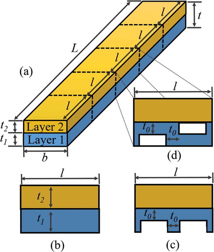
Thermal stress in layered structure subjected to temperature change has been studied over half a century [Citation5,Citation6]. Analytical stress calculations have been well studied in terms of residual stress, shear stress and thermal deflection [Citation7–Citation9] With the rapid development of MEMS multilayered electronic components in the 1980s, more attention has been focused on the thermal and residual stresses predictions [Citation4]. The interfacial shear stress and peeling stress has also been explored [Citation10]. As shown in ), a standard bi-material strip is comprised of two perfectly-bonded material components, indicated as Layer 1 and Layer 2. The strip is L in length and b in width. The layer thicknesses of Layer 1 and Layer 2 are defined as t1 and t2, respectively. The Young’s modulus and coefficient of thermal expansion (CTE) of Layer 1 and Layer 2 are defined as ,
,
and
, respectively. In this study, three design patterns are considered along the axial direction of the strip: standard design; E-shape design; and S-shape design, as shown in -d), respectively. For the E-shape design and S-shape design, two design parameters are considered: the periodic cell length l and the wall thickness t0.
Figure 1. Schematics of (a) a bi-material strip with three design patterns: (b) standard design; (c) E-shape design; (d) S-shape design.
For the bi-material strip with standard design, the analytical solution of the curvature κ when subjected to temperature variation is defined as [Citation11]
where is the radius of curvature. Equation (1) is valid under the following assumptions: (1) Layer 1 and Layer 2 are perfectly bonded at the interface; (2) a linear strain distribution existed through the thickness direction; (3) the curvature is constant along the strip; (4) the beam thickness t is much smaller than the radius of curvature r; and (5) the elongation of the strip is negligible along the axial direction.
Taking the ratio of the two layer materials in terms of the Young’s modulus , thickness
, and CTE
, Equation (1) can be expressed as:
When the bi-material strip is treated as a cantilever beam, the deflection at the free end can be defined as
In Equation (2), the curvature is independent of the magnitude of the materials’ Young’s modulus and the width of the strip. It shows a linear relationship with the CTE of the materials and the temperature variation. The larger the temperature variation/CTE difference, the larger the curvature
reaches. The curvature
is in a reciprocal relation with the thickness of the bi-material strip. The thinner the strip, the larger the curvature can be. However, with same overall thickness t, the relation among the curvature
, thickness ratio
and modulus ratio
are complicated. In order to achieve the maximized curvature of the bi-material strip, the derivative of curvature
with respect to
and
is set to be zero. When
and
satisfies
the curvature reaches its maximum value.
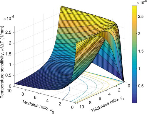
To visualize this relation, we define the CTE of Layer 1 and Layer 2 as α1 = 2.8e-6/°C and α2 = 14e-6/°C then adopt Equation (2) to plot the temperature sensitivity () as a function of modulus ratio,
, and thickness ratio,
, shown in . The curvature
is very sensitive to
and
, when
and
are less than 1. There exists an optimal thickness ratio and modulus ratio to maximize the curvature sensitivity when
and
satisfy the relation in Equation (4). Therefore, for a bi-material strip with standard solid cross-section and pre-selected material properties (
,
,
and
), and strip geometry properties (t, b, L), the thickness ratio can be designed to satisfy Equation (4) in order to reach to the maximum temperature sensitivity.
Figure 2. Curvature variation with respect to modulus ratio and thickness ratio of the bi-material strip.
Numerical modeling and discussion
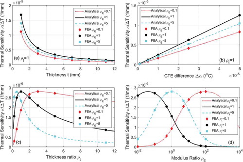
In this section, finite element analysis (FEA) is performed through ABAQUS [Citation12] to investigate the thermo-mechanical coupling multi-physics problem of the bi-material strip under temperature variation. In the FEA model, we define the geometry properties of the bi-material strip as L = 300mm, t = 6mm, b = 6mm, and the material properties of Layer 1 and Layer 2 materials as α1 = 2.8e-6/°C, α2 = 14e-6/°C, and E1 = 80GPa, unless it is defined separately in the following discussion. The convergence study has been performed with respect to the element type selection and element size selection. The quadratic volume element is selected for better accuracy and efficiency purpose.
For a bi-material strip based temperature sensor, the design parameters include material selections (α1, α2, E1, and E2) and geometry design (L, b, t, t1, and t2). As shown in , we perform the numerical analysis based on the FEA model described above to investigate the temperature sensitivity (κ/∆T) variation with respect to the thickness ratio, ρt, modulus ratio, , beam thickness, t, and CTE difference, ∆α. Both the FEA numerical simulation results and the analytical solutions from Equation (2) are presented. It is clear that the FEA results match well with the analytical solutions, which prove the accuracy of the FEA modeling. (a) presents the reciprocal relation between thermal sensitivity and the beam thickness under various modulus ratio. In order to achieve higher thermal sensitivity, thinner bi-material strip thickness are desired. ) presents the linear relationship between thermal sensitivity and the CTE difference with respect to various modulus ratios at t = 6mm. In order to achieve higher thermal sensitivity, larger CTE differences between two materials are desired. ,d) present the relation among thermal sensitivity (κ/∆T), thickness ratio, ρt, and modulus ratio,
at t = 6mm. It is clear that the thermal sensitivity is more sensitive to the thickness ratio than the modulus ratio. When
and
satisfy the relation in Equation (4), the maximized thermal sensitivity is achieved.
Figure 3. Thermal sensitivity variation with respect to different design parameters: (a) thickness; (b) CTE difference; (c) thickness ratio; and (d) modulus ratio.
With the capability of additive manufacturing, complex structure design can be introduced in bi-material strip design to achieve better temperature sensitivity. As shown in ,d), we propose two periodic pattern designs along the axial direction of the strip: E-shape design and S-shape design. The periodic representative volume cell length is defined as l. The wall thickness, t0, is associated with volume fraction,, which is defined as
, representing the ratio of empty space of the unit cell along the axial direction. When
, both E-shape and S-shape designs converge to the standard design.
The design parameters for the bi-material strip with periodic patterns along the axial direction includes material property selections (α1, α2, E1, and E2), overall geometry parameters (L, b, t, t1, and t2), and the pattern feature parameters (, l, and
). In order to understand the pattern feature design parameters, we systematically conduct a series of FEA simulations based on three pattern designs: standard (denoted as std.), E-shape pattern (denoted as E-shape) and S-shape pattern (denoted as S-shape) with the following material properties and overall geometry parameters: t = 6mm, L = 30mm, l = 6mm, α1 = 2.8e-6/°C, α2 = 14e-6/°C, E1 = 80GPa, and ∆T = 50°C. In order to emphasis the advantages of patterned design on temperature sensitivity enhancement, the normalized deflection variation (δ/δstd max) with respect to thickness ratio, and volume fraction are presented in -, with respect to various modulus ratios. δ presents the defection of the bi-material strip as a cantilever beam, δstd max presents the maximum deflection of the bi-material cantilever beam with given material properties with the standard pattern design. In -, the normalized deflection for standard design, E-shape design and S-shape design are presented as the height of the blue, cyan and green color bars, respectively. The red color bars with the unit length present the optimized parameters (ρt, and ρE) selection of the standard design.
Figure 4. Normalized deflection variation of three design patterns with respect to ρt and volume fraction Vf at ρE = 0.1.
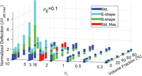
Figure 5. Normalized deflection variation of three design patterns with respect to ρt and volume fraction Vf at ρE = 1.
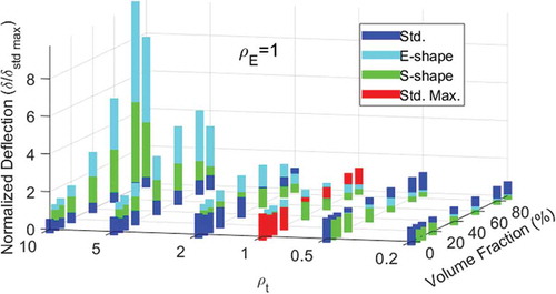
Figure 6. Normalized deflection variation of three design patterns with respect to ρt and volume fraction Vf at ρE = 10.
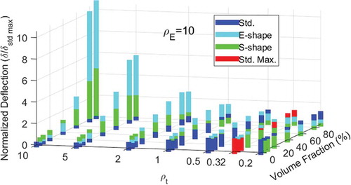
When the thickness ratio is less than the optimized value in Equation (4) with respect to the corresponding modulus ratio, the standard pattern design always brings the largest normalized deflection, shown in -. When the thickness ratio is larger than the optimized value with respect to the corresponding modulus ratio, E-shape design and S-shape design present the great potential in enhancing the temperature sensitivity as the normalized deflection is greatly enhanced. The normalized deflection variation of E-shape design and S-shape design does not follow any monotonic trend with respect to the thickness ratio and volume fraction. With higher thickness ratio and volume fraction, the E-shape design can increase the maximum deflection of the standard design by more than 8 times. In most of the cases when thickness ratio is larger than the optimized value, E-shape design is the best design among the three design patterns. However, S-shape design presents the highest normalized deflection in with high thickness ratio and low volume fraction.
The high performance of E-shape design is mainly due to the periodic reduction of the total thickness along the strip’s axial direction. As shown in ), the strip thickness is reduced to t = t0+ t2 in some of the segment along the axial direction. With the temperature variation, the bi-material strip is deformed due to the thermal stress induced from the thermal expansion coefficient difference between the two materials. However, the ‘teeth’ part of Layer 1 in the E-shape design barely contributes the deformation of the bi-material strip. Therefore, the effective thickness of Layer 1 could be assumed to be t0. The reciprocal relation between the curvature, κ, and thickness, t, in Equation (2) then leads to great increase of curvature (therefore deflection) with respect to the deduction of the thickness t. To approximate the curvature and deflection variation of the E-shape design, we ignore the ‘teeth’ part of Layer 1 in the E-shape design and define the effective thickness of the bi-material strip as
The effective thickness ratio is defined as
Therefore the effective curvature of the E-shape design can be defined as
The deflection of the bi-material strip with E-shape design is then evaluated by Equation (3).
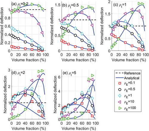
presents the normalized deflection comparison between the analytical predictions in Equations (5–7) and the FEA results, with respect to the original thickness ratio, modulus ratio and volume fraction. The blue lines present the analytical prediction through Equation (5–7). The colorful symbols present the FEA results. It is clear that the analytical prediction matches well with the numerical results when ρt < 1, regardless of the modulus ratio and the volume fraction, shown in -c). When ρt > 1, the analytical prediction matches well with the FEA results when volume fraction is less than 50%, regardless of the modulus ratio. Error appears under high thickness ratio and high volume fraction cases, shown in ). It is because the effective thickness assumption is no longer accurate under such a high thickness ratio and volume fraction conditions.
Figure 7. Normalized deflection variation comparison between analytical prediction and FEA simulation of E-shape design, with respect to volume fraction, thickness ratio and modulus ratio.
Therefore, for a bi-material strip with periodic pattern design along the axial direction, more design and optimization space is available to achieve high temperature sensitivity. With selected material properties (,
,
and
), and overall strip geometry properties (t, b, L), optimized pattern feature parameters (
, l, and
) would be selected to maximize the temperature sensitivity with the consideration of additive manufacturing capability, material strength.
Conclusions
The rapid development of additive manufacturing technologies bring great potential to enhance multi-layer structure design for better functionality. In this work, we adopt the bi-material strip temperature sensor as an example to prove the concept of the enlarged design space with the capability and feasibility of additive manufacturing. Through both analytical modeling and numerical simulations, we considered three pattern designs: standard, E-shape and S-shape. The E-shape design pattern greatly enhances the temperature sensitivity of the bi-material strip. An analytical formulation is proposed to predict the temperature sensitivity of E-shape design. The accuracy is validated through the comparison with the numerical modeling results. This concept can be further applied to multi-layered structure and material design in the area of microelectronics, structural engineering, and aerospace engineering to further enhance the high performance functionality of the structures and materials in various length scales.
Acknowledgments
We gratefully acknowledge support from the Office of Energy Efficiency and Renewable Energyunder the contract DE-EE-0007683 by Department of Energy.
Disclosure statement
No potential conflict of interest was reported by the authors.
Additional information
Funding
References
- W. Riethmuller and W. Benecke, Thermally excited silicon microactuators, IEEE Trans. Electron. Devices 35 (6) (1988), pp. 758–763. doi:10.1109/16.2528.
- A. Atkinson and P.T. Moseley, Thin film electroceramics, Appl. Surf. Sci. 65/6 (1993), pp. 212–219. doi:10.1016/0169-4332(93)90661-T.
- S. Nikbakt, S. Kamarian, and M. Shakeri, A review on optimization of composite structure Part I: Laminated composites, Compos. Struct. 195 (2018), pp. 158–185. doi:10.1016/j.compstruct.2018.03.063.
- S. Singamaneni, M.C. LeMieux, H.P. Lang, C. Gerber, Y. Lam, S. Zauscher, P.G. Datskos, N.V. Lavrik, H. Jiang, R.R. Naik, T.J. Bunning, and V.V. Tsukruk, Bimaterial Microcantilevers as a Hybrid Sensing Platform, Advanced Mater. 20 (2008), pp. 653–680. doi:10.1002/(ISSN)1521-4095.
- G.G. Stoney, The tension of metallic films deposited by electrolysis, Proc. Royal Soc. A 82 (1909), pp. 172. doi:10.1098/rspa.1909.0021.
- S. Timoshenko, Analysis of bi-metal thermostats, J. Opt. Soc. Am. 11 (1925), pp. 233. doi:10.1364/JOSA.11.000233.
- J.W. Eischen and J.S. Everett, Thermal stress analysis of bimaterial strip subject to axial temperature gradient, J. Electron. Packaging 111 (1989), pp. 282. doi:10.1115/1.3226548.
- J.W. Eischen, C. Chung, and J.H. Kim, Realistic modeling of edge effect stresses in biomaterial elements, J. Electron. Packaging 112 (1990), pp. 16. doi:10.1115/1.2904333.
- H. Torun and H. Urey, Thermal deflections in multilayer microstructures and athermalization, J. Appl. Phys. 100 (2006), pp. 023527. doi:10.1063/1.2216789.
- X. Zhang, Z. Hu, and Y. Li, Bending of bi-gels, J. Chem. Phys. 105 (1996), pp. 3794. doi:10.1063/1.472200.
- C.-H. Hseueh, Modeling of elastic deformation of multilayers due to residual stresses and external bending, J. Appl. Phys. 91 (2002), pp. 9652. doi:10.1063/1.1478137.
- ABAQUS, ABAQUS/CAE 6.11 User’s Manual, 2018. Online Documentation Help: Dassault Systèmes, retrieve from https://www.3ds.com/products-services/simulia/products/abaqus/.