
 ?Mathematical formulae have been encoded as MathML and are displayed in this HTML version using MathJax in order to improve their display. Uncheck the box to turn MathJax off. This feature requires Javascript. Click on a formula to zoom.
ABSTRACT
For single-walled carbon nanotubes (SWCNTs) with a length of 1–50 µm, the surface plasmon-polariton (SPP) resonance is within the terahertz frequency range; therefore, SWCNT lattices can be used to design frequency-selective surface (FSS). A numerical model of electromagnetic wave diffraction on a two-dimensional periodic SWCNT lattice can be described by an integro-differential equation of the second-order with respect to the surface current along SWCNT. The equation can be solved by the Bubnov–Galerkin method. Frequency dependence of reflecting and transmitting electromagnetic waves for FSSs near the SPP resonance is studied numerically. It is shown that the resonances are within the lower-frequency part of the terahertz range. We also estimate the relaxation frequency of an individual SWCNT and demonstrate the applicability of the Kubo formula for graphene conductivity to array of strips similar in size to SWCNTs under consideration.
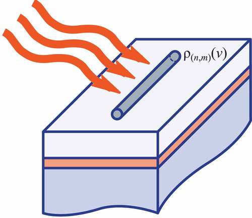
Graphical abstracts
1. Introduction
Single-walled carbon nanotube (SWCNT) is a seamless cylinder that can be represented as a result of rolling up of a flat hexagonal graphene strip [Citation1,Citation2]. The SWCNT diameter ranges from one to several tens of nanometers, whereas the length can reach a millimeter size. Orientation of the honeycomb graphene lattice with respect to nanotube axis determines an important structural characteristic, i.e. chirality. More precisely, the chirality is characterized by two integer indices known as chiral vector and indicating the location of the lattice hexagon which, as a result of the tube rolling up, shall coincide with the hexagon at the origin [Citation3]. If the difference of the chirality indices is divisible by 3, the nanotube is metallic; otherwise, it is semiconductor [Citation4,Citation5]. In addition to the type of conductivity, the bandgap that is an important characteristic of electronic properties of semiconducting nanotubes is also determined by the SWCNT chirality [Citation6].
Carbon nanotubes can be applied to the surface of any shape [Citation7–12]. This leads to the opportunity to manufacture high-performance absorbers [Citation13–15] and frequency-selective surfaces (FSS) [Citation16,Citation17] with desired reflecting and absorbing bands, representing a biperiodic grating of nanotubes located on a layered substrate. Due to the large length-to-diameter ratio and sufficiently high conductivity, electric fields with a high time-averaged strength arise in the resonance region near the relaxation frequency of the nanotube. According to Ref [Citation18], the resonant frequencies of SWCNTs lie within the lower-frequency part of the sub-terahertz range. Devices operating in this range are widely used in various fields from astrophysics, ecology, and environmental monitoring in order to examine high-purity substances, communication and security systems, and so on. Due to the promising properties of nanotubes, the size of nanotube-based diffraction lattices is expected to be an order of magnitude smaller than similar gratings based on metal strips.
The design of these devices has a high priority and requires strict electrodynamic modeling. However, the study of heterostructures by direct grid methods in the variational (finite element method, method of moments) and differential (finite difference method) formulations encounters a number of difficulties associated with the application of these methods to semi-infinite layers, periodic and open boundaries. Construction of the tensor Green’s function for Maxwell’s equations in a layered medium and solution of the vector integral equations by the Bubnov-Galerkin projection method is the most rigorous approach for numerical modeling this problem [Citation19–21]. In contrast to the latter papers, we note that in the diffraction problems, the transverse current in the SWCNT can be neglected.
In this paper, the diffraction of electromagnetic waves on a two-dimensional periodic grating of SWCNTs placed on a multilayered substrate is studied. The substrate can be made up of dielectric, metal, and graphene layers.
In the considered theory of SWCNT diffraction, it was assumed that the following surface impedance boundary condition [Citation22] is satisfied on the nanotube surface:
where and
are the longitudinal components of the electric field strength and surface current density:
where is the magnetic field strength,
is the normal unit vector to the surface of SWCNT,
is the surface resistance of the carbon nanotube [Citation22]:
where is the Fermi velocity,
is the cyclic frequency,
is the electron charge,
is the Planck constant,
is the relaxation frequency,
is the nanotube radius, which is expressed through chirality indices
as:
where nm is the distance between adjacent carbon atoms in the graphite plane.
EquationEquation (2)(2)
(2) is applicable for metallic SWCNTs. It was obtained by G. Y. Slepyan [Citation22] in the approximation of the Boltzmann relaxation equation. The derivation of this equation with a generalization for the case of semiconductor nanotubes is given in the Appendix. It should be noted that an additional factor
(14) appears in the denominator (2) for semiconductor SWCNTs. For instance, for semiconductor SWCNTs with radii ,α ∈ [2.68 Å(6,1),
,
varies within the range
,
.
EquationEquation (2)(2)
(2) corresponds to the sum of the successive effective inductive and active resistances. The equation for the active resistance contains a phenomenological parameter
and requires further discussion. Due to the use of the Boltzmann relaxation equation in Ref [Citation22], the active resistance, similar to the Drude model [Citation23], is proportional to the inverse of the relaxation time. The parameter
in Ref [Citation22] is equal to
Hz.
Short metallic SWCNTs are one-dimensional quantum conductors in which the ballistic conductivity activity can take place [Citation24–26]. This is a phenomenon in which the scattering of charges occurs only at the ends of the conductor, whereas the conductor conductivity is constant and depends on neither the length nor the radius of the conductor. The SWCNT band structure is determined by two Dirac cones [Citation6,Citation27]; therefore, in the ballistic mode, the SWCNT conductivity is equal to two quanta of conductivity [Citation25,Citation26] (the value of one quantum is equal to ). However, a resistance of the order of
is observed for SWCNTs with a length significantly less than
and increases essentially for long nanotubes. For instance, in Ref [Citation28], the SWCNT resistance was measured at direct current. In particular, a metallic SWCNT with a length
µm has a resistance
at room temperature. If we use the experimental results [Citation28], then for nanotubes with a length of
µm for the relaxation frequency of metallic SWCNTs we obtain the following:
Therefore, the value of in Ref [Citation22] seems for us to be underestimated.
A random sample of SWCNTs contains approximately a third of metallic ones. According to our estimate (see Appendix Equationequation (13)(13)
(13) ), in the terahertz range the resistance of semiconductor nanotubes is several orders of magnitude larger. Therefore, the two-dimensional periodic grating contains only metallic SWCNTs in the layered heterostructures considered in this article.
2. Theory
In this paper, a study of diffraction on heterostructures of two types with a two-dimensional periodic grating is presented. The unit cell of the first structure, shown in , consists of SWCNT 1 with radius and length
placed on a dielectric layer 2 with thickness
and metallic layer 3 with thickness
deposited on the surface of a semi-infinite dielectric substrate. The introduced Cartesian rectangular coordinate system has its origin located in the middle of the SWCNT; the z-axis is directed along the normal to the substrate surface, and the y-axis is oriented along the nanotube symmetry axis. In the second structure, there is no metallic layer (
).
Figure 1. (Color online) Geometric model of a frequency-selective surface: 1 – one unit cell of the two-dimensional periodic SWCNT grating, 2 – dielectric layer, 3 – metallic layer, 4 – semi-infinite dielectric substrate.
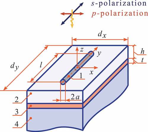
Several SWCNTs can be placed parallel to each other in one unit cell in order to estimate the amplitude-frequency characteristics in the case of random distribution of SWCNT sizes. The geometrical parameters of each SWCNT and the distance between them are determined using a random number generator.
The electric field generated by currents flowing on the nanotube surface
is determined as follows:
where is the tensor Green’s function. For a multi-layered media, it is defined by Ref [Citation20]. The SWCNT length is three orders of magnitude larger than its radius; therefore, only the longitudinal component of the surface current
can be taken into account in SWCNTs.
Substituting (3) into (1), the integro-differential equation is obtained:
where the observation points in the cylindrical coordinate system (,
,
) and the source points (
,
,
) are located on the SWCNT surface (
,
);
is the external electromagnetic field (the field in a multilayer structure without SWCNT taken into account when a plane electromagnetic wave is incident). Obtaining
is a simple issue [Citation19].
For a two-dimensional periodic grating of SWCNTs placed on the surface of a multilayered substrate, with periods and
, the Green’s function can be written as a series. The component
of the tensor Green’s function has the following form:
where ,
,
and
are the projections of the wave vector of the incident wave, the function
in each of the layers satisfies the equation:
where is constant within each layer,
is Dirac’ delta function. It should be noted that the transverse component of the current can be neglected, since the SWCNT length is several times larger than its diameter.
In Ref [Citation19], the tensor Green’s function was constructed satisfying EquationEquation (5)
(5)
(5) and the continuity condition for tangential components of the electric field strength. The recurrence equations for
in Ref [Citation19] can be used for an arbitrary number of layers and are protected from overflow.
In our study, the SWCNTs are located on the surface of a multilayered substrate. In this case, the solution (5) in the upper layer is the function:
The algorithm proposed in Ref [Citation19]. is used to determine the constants 0;mn.
EquationEquation (4)(4)
(4) is solved by the Bubnov-Galerkin projection method. The current density function
is approximated by a linear combination of the basis functions:
where is Gegenbauer polynomial (ultraspherical polynomial),
is unknown coefficients, the values
are selected so that the condition is satisfied:
where is Bessel function of the first kind.
Using the projection method, a system of linear equations of order with respect to the unknowns
is obtained. The matrix elements in the system of linear equations contain a double integral over the SWCNT surface, which is calculated numerically. The left side of Equationequation (3)
(3)
(3) is used to find the reflected and transmitted waves.
A system of linear equations has good convergence. Usually, it is sufficient to solve a fifth-order system for calculations with an internal convergence error of 0.5%. The time of numerical calculation at a given frequency is less than 0.5 s on 1 core of Intel Core [email protected] GHz.
3. Results and discussion
Below we present the results of a computational study of the diffraction of electromagnetic waves with -polarization (the electric field is directed along the SWCNT) and
-polarization (the electric field is directed across the SWCNT) for two types of frequency-selective surfaces (FSS1 without metallic layer and FSS2 with thin one) shown in .
Both types of FSS contain SWCNTs with chirality indices (31, 31) and the radius nm, which form a two-dimensional periodic grating with periods
µm and
µm. The nanotubes have a length
µm. The SWCNT relaxation frequency is
Hz. Zinc Oxide with a refractive index
is selected as the material of the semi-infinite dielectric substrate 4.
The first structure (FSS1) is transmissive with a minimum transmission coefficient at wave resonance with
-polarization and
for a wave with
-polarization. There is no metallic layer 3 in FSS1. In order to realize a quarter-wavelength coating, a dielectric layer 2 with a refractive index
(approximately equal to that in SiO2) is used. The layer has a thickness that approximately equals to a quarter of the wavelength for the insulation material at the resonant frequency.
The second structure (FSS2) is reflective with a minimum reflection coefficient at wave resonance with
-polarization and
for a wave with
-polarization. Metallic layer Au with a thickness
µm and conductivity similar to that of a bulk material was selected as a reflective metallic film 3. The choice of dielectric layer 2 is similar to the case of FSS1 except for a slightly different refractive index
.
It should be noted that for FSS2 structure, instead of a metallic mirror, it is possible to realize a dielectric mirror, consisting of several alternating quarter-wave dielectric layers.
shows the amplitude-frequency characteristics of the power reflection and transmission
coefficients for FSS1, whereas
is the absorption coefficient. The
and
indices denote the type of wave polarization. The circular resonant frequency is
times greater than
.
Figure 2. (Color online) Amplitude-frequency characteristics of the power reflection , transmission
, and absorption
coefficients for FSS1 heterostructure when
- and
-polarization are considered.
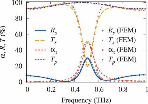
In the resonance region, a -polarized wave passes through the grating without reflection. The transmission coefficient of a
-polarized wave may be less than
. It should be noted that the length of an equivalent metallic half-wave oscillator at a frequency
THz is approximately 300 µm, which is
times greater than for SWCNTs.
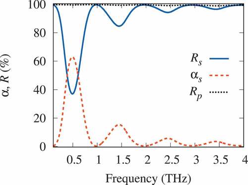
The paper further considers the effect of losses on the frequency characteristics of the reflection coefficient for FSS1 heterostructure (). Similar to a simple oscillator, increasing the loss () extends the resonant curve without changing the resonant frequency. Thus, if our estimate
is correct, then the resonance on long SWCNTs is fairly well pronounced at room temperature.
Figure 3. (Color online) frequency dependence of the transmission coefficient for FSS1 heterostructure at different SWCNT relaxation frequencies with SWCNTs length (a)
µm, (b)
µm.
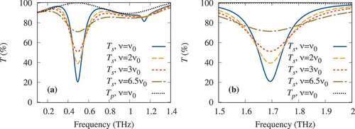
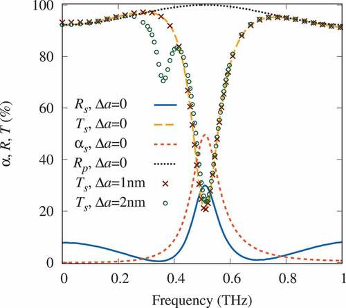
shows the frequency characteristics of the transmission coefficient for FSS1 with SWCNT length
µm and unit cell periods
µm,
µm. Since SWCNT surface resistance depends on the frequency, the scalability principle is not observed. Shortening SWCNTs by ten times (from
to 2 µm) increases the resonance frequency by approximately
times. The circular resonant frequency is
times greater than
. The width of the resonance curve almost remains unchanged. Due to the higher frequency, the Q-factor of the resonance is higher for short SWCNTs.
show the amplitude-frequency characteristics of FSS2 structure. When the incident electromagnetic wave is -polarized, the grating is an almost perfect mirror. In the resonance region of the
-polarized wave, the losses in both the SWCNT and the metallic film increase significantly. When the thickness of the dielectric layer is equal to
–
of the wavelength, the incident power on the SWCNT and the reflected one from the metallic layer (Au) are added in phase at the resonant frequency. The higher resonances are poorly pronounced.
Figure 4. (Color online) Frequency dependence of the reflection and absorption
coefficients for FSS2 heterostructure with the lattice period
,
, SWCNT length
, the dielectric layer thickness (a)
, (b)
.
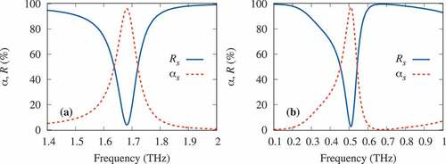
Figure 5. (Color online) Frequency dependence of the reflection and absorption
coefficients for FSS2 heterostructure at the relaxation frequency
.
With an increase in the relaxation frequency , the level of the main resonance decreases and higher resonances appear (). They are due to the large reflection coefficient (from SWCNTs) of standing electromagnetic wave in the dielectric layer.
To estimate the amplitude-frequency characteristics in the case of a random distribution of SWCNT sizes, it is assumed that the unit cell contains an number of SWCNTs. The geometrical parameters of each SWCNT and the distance between them are determined by a random number generator. The following parameters are additionally set for calculations of such structure:
• average distance between nanotubes (µm) and its maximum deviation
(µm),
• maximum deviation of the nanotube radii (µm),
• maximum deviation of the nanotube length (µm),
• maximum deviation of the angles of inclination of nanotubes to the -axis.
shows the amplitude-frequency dependence of the FSS1 heterostructure containing identical SWCNTs (curves with ) and those characterized by a random distribution of geometrical parameters. A small deviation from the average value of the SWCNT radii (
µm,
nm, red cross-shaped markers) has an extremely weak effect on the resonance position. In the case of a scatter of SWCNT lengths (
µm,
nm, green circle-shaped markers), the main resonance also changes weakly, and well-pronounced additional resonances appear. Their position and depth are highly dependent on the magnitude
.
Figure 6. (Color online) Amplitude-frequency dependence of the FSS1 heterostructure with a random scatter of SWCNT sizes.
The paper further compares the characteristics of SWCNT FSS with the characteristics of similar FSS formed by graphene strips. The surface resistance of graphene can be described by the Kubo formula [Citation29]. This formula is also used when calculating µm-sized graphene strips. At nanometer sizes, size effects shall occur.
When graphene is rolled up into a nanotube, size effects also occur, and the Kubo formula for SWCNTs may not be applicable. However, it should be expected that the resonant frequencies lie in the same frequency range. To verify this statement, FSS1 and a similar heterostructure were calculated, where graphene strips [Citation30] are used instead of nanotubes. The lengths of strips and SWCNTs are the same and equal to 20 µm. The width of strip is equal to the diameter of the nanotube
(
eV,
ps,
K). The resonances of FSS based on graphene strips depend on the relaxation time
and chemical potential
, which can be controlled by applying gate voltage and chemical doping. At room temperature
K (
eV,
ps), these resonances lie in the same frequency range as FSS resonances from SWCNTs.
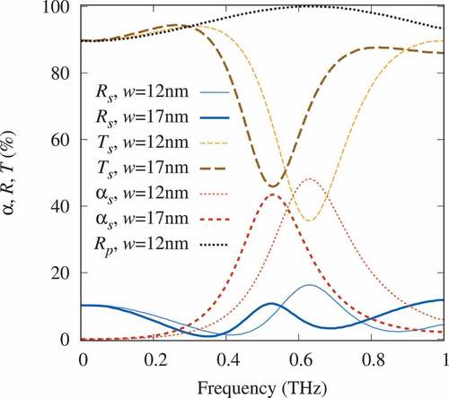
shows the amplitude-frequency characteristics of a two-dimensional periodic grating of graphene strips with a width of nm and
nm. Since SWCNTs are located in the air and the graphene strip lies on an insulation material, it can be assumed that the above estimate of the strip width is overestimated. The resonant frequency of this grating almost completely coincides with the resonance frequency of the CNT grating (), whereas the frequency characteristics are close to the FSS1 characteristics of CNTs at
.
Figure 7. (Color online) Amplitude-frequency characteristics of a two-dimensional periodic grating of graphene strips with a width of nm and
nm.
4. Conclusion
The theory of constructing the tensor Green’s function for Maxwell’s equations solved by the Bubnov-Galerkin projection method was developed for the numerical electrodynamic simulation of electromagnetic wave diffraction on a two-dimensional periodic grating of SWCNTs and graphene strips located on a multilayered substrate. On the basis of the Bubnov–Galerkin method, algorithms for numerical calculation, and software were developed for mathematical modeling of electromagnetic wave diffraction on heterostructures with two-dimensional periodic SWCNT grating. The presence of a surface plasmon-polariton resonance on SWCNTs in the terahertz range was shown. The amplitude-frequency dependence of resonant-reflecting and resonant-transmitting frequency-selective surfaces was calculated. A model of diffraction grating with a random scatter of SWCNT sizes was studied. The frequency characteristics of frequency-selective surfaces for SWCNTs and graphene strips were compared.
Data availability
The data that support the findings of this study are available from the corresponding author upon reasonable request.
Disclosure statement
No potential conflict of interest was reported by the author(s).
Additional information
Funding
References
- Saito R, Dresselhaus G, Dresselhaus MS. Physical properties of carbon nanotubes, published by Imperial College Press and distributed by World Scientific Publishing Co. 1998.
- Jorio A, Dresselhaus G, Dresselhaus MS, eds. Carbon nanotubes, topics in applied physics. Vol. 111. Berlin Heidelberg Berlin Heidelberg: Springer; 2008.
- Dresselhaus M, Dresselhaus G, Saito R. Physics of carbon nanotubes. Carbon N Y. 1995;33(7):883–891.
- Saito R, Fujita M, Dresselhaus G, et al. Electronic structure of chiral graphene tubules. Appl Phys Lett. 1992;60(18):2204–2206.
- Saito R, Dresselhaus G, Dresselhaus MS. Trigonal warping effect of carbon nanotubes. Phys Rev B. 2000;61(4):2981–2990.
- Samsonidze GG, Saito AR, Jorio DA, et al. The concept of cutting lines in carbon nanotube science. J Nanosci Nadoichnol. 2003;3(6):431–458.
- Single-walled carbon nanotubes, topics in current chemistry collections editors Li Y, Maruyama S. Cham: Springer International Publishing, 2019.
- Rao SG, Huang L, Setyawan W, et al. Large-scale assembly of carbon nanotubes. Nature. 2003;425(6953):36–37.
- Che G, Lakshmi BB, Martin CR, et al. Chemical vapor deposition based synthesis of carbon nanotubes and nanofibers using a template method. Chem Mater. 1998;10(1):260–267.
- Kholghi Eshkalak S, Chinnappan A, Jayathilaka W, et al. A review on inkjet printing of CNT composites for smart applications. Appl Mater Today. 2017;9:372–386.
- Gao S, Zhao X, Fu Q, et al. Highly transmitted silver nanowires-swcnts conductive flexible film by nested density structure and aluminum-doped zinc oxide capping layer for flexible amorphous silicon solar cells. J Mater Sci Technol. 2022;126:152–160.
- Wang P, Song T, Abo-Dief HM, et al. Effect of carbon nanotubes on the interface evolution and dielectric properties of polylactic acid/ethylene–vinyl acetate copolymer nanocomposites. Adv Compos Hybrid Mater. 2022;5(2):1100–1110.
- Xiao D, Zhu M, Sun L, et al. Flexible ultra-wideband terahertz absorber based on vertically aligned carbon nanotubes. ACS Appl Mater Interfaces. 2019;11(46):43671–43680.
- Luo F, Liu D, Cao T, et al. Study on broadband microwave absorbing performance of gradient porous structure. Adv Compos Hybrid Mater. 2021;4(3):591–601.
- Zhang Z, Zhao Y, Li Z, et al. Synthesis of carbon/sio2 core-sheath nanofibers with co-fe nanoparticles embedded in via electrospinning for high-performance microwave absorption. Adv Compos Hybrid Mater. 2022;5(1):513–524.
- Matsumoto K, ed. Frontiers of graphene and carbon nanotubes. Tokyo: Springer Japan; 2015.
- Cao Q, Rogers JA. Ultrathin films of single-walled carbon nanotubes for electronics and sensors: a review of fundamental and applied aspects. Adv Mater. 2009;21:29–53.
- Melnikov AV, Kuzhir PP, Maksimenko SA, et al. Scattering of electromagnetic waves by two crossing metallic single-walled carbon nanotubes of finite length. Phys Rev B. 2021;103(7):075438.
- Lerer AM. Theoretical investigation of 2D periodic nanoplasmon structures. J Commun Technol Electron. 2012;57(11):1151–1159.
- Lerer AM, Makeeva GS, Cherepanov VV. Nonlinear interaction of terahertz waves with nanostructured graphene in resonance multilayer plasmon structures. J Commun Technol Electron. 2021;66:656–664.
- Hao J, Hanson GW. Optical scattering from a planar array of finite-length metallic carbon nanotubes. Phys Rev B. 2007;75(16):165416.
- Slepyan GY, Maksimenko SA, Lakhtakia A, et al. Electrodynamics of carbon nanotubes: dynamic conductivity, impedance boundary conditions, and surface wave propagation. Phys Rev B. 1999;60(24):17136–17149.
- Drude P. Zur Elektronentheorie der Metalle. Ann Phys. 1900;306(3):566–613.
- Landauer R. Electrical resistance of disordered one-dimensional lattices. Philos Mag. 1970;21(172):863–867.
- Frank S, Poncharal P, Wang ZL. Carbon Nanotube Quantum Resistors. Science. 1998;280(80):1744–1746.
- Kong J, Yenilmez E, Tombler TW, et al. Quantum interference and ballistic transmission in nanotube electron waveguides. Phys Rev Lett. 2001;87(10):106801.
- Ando T. Theory of electronic states and transport in carbon nanotubes. Journal of the Physical Society of Japan. 2005;74(3):777–817.
- Li S, Yu Z, Rutherglen C, et al. Electrical properties of 0.4 cm long single-walled carbon nanotubes. Nano Lett. 2004;4(10):2003–2007.
- Hanson GW. Dyadic Green’s functions and guided surface waves for a surface conductivity model of graphene. J Appl Phys. 2008;103(6):064302.
- Lerer AM, Makeeva GS. Controlled absorbers for terahertz spectral range based on resonance absorption in periodic multilayer graphene structures. Tech Phys Lett. 2018;44(9):852–855.
Appendix A.
Extended Slepyan-Hanson theory
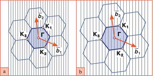
The reciprocal space of any SWCNT is a set of parallel equidistant cutting lines lying within the first Brillouin zone (FBZ) of graphene [Citation6] (). The cutting lines are numbered by index and directed along the axis of the nanotube. Their number is equal to the number of hexagons per SWCNT period, and the distance between lines equals
, where
is the nanotube perimeter. The equilibrium Fermi-Dirac distribution for electrons in SWCNTs is as follows [Citation27]:
Figure A1. (Color online) The first and adjacent Brillouin zones in reciprocal space of graphene with superimposed cutting lines: (a) – metallic SWCNT, (b) – semiconductor SWCNT. The vertices of hexagons correspond to the points , where the electron dispersion is characterized by a Dirac cone and a constant group velocity
. Each point
is divided between three adjacent zones, so the first Brillouin zone has two non-equivalent points
. The marked points
,
, and
are equivalent with respect to the translations of the reciprocal space.
where is the dependence of the electron energy on the wave vector for the cutting line with index
,
is the Boltzmann constant,
is the absolute temperature, and the chemical potential µ in the issue under consideration is zero. The factor
appears in the numerator, since two electrons per graphene unit cell participate in the formation of the band structure, and, accordingly, the state
simultaneously corresponds to two different spin orientations.
The paper further considers the non-equilibrium electron distribution . This distribution occurs in an external alternating electric field. Unlike the usual Fermi–Dirac distribution
, it depends on time
and coordinate
directed along the nanotube. Following Ref [Citation22], the Boltzmann relaxation equation can be written as follows:
where the relaxation processes are taken into account in the right part of the equation; the electric field is directed along the SWCNT axis,
is the force that changes the quasimomentum of the electron
,
is its velocity,
is the wave number of the electron, and
is the relaxation frequency.
Rewriting in (6) as the sum of the equilibrium
and non-equilibrium distribution
we obtain the following differential equation:
It is assumed that the electric field changes in time according to the harmonic law along -axis. Substituting into (7) the expressions
,
, and
, the following equation is obtained
Rearrangement of Equationequation (8)(8)
(8) leads to the following:
In the issue under consideration, the value is limited by the Fermi velocity
of electrons in graphene. The contribution of the small term
in the denominator can be neglected [Citation29]. The amplitude of the total electron current
can only be related to the amplitude of the non-equilibrium part of the distribution
:
where is the electron group velocity and
is the SWCNT length. Taking into account in (10) that
we obtain the following:
The valence band in SWCNTs is symmetric with the conduction band. Assuming the relaxation time for holes is the same as for electrons, and taking into account the hole current in the valence band (equal to ), we use the integration over the wave number and rewrite the amplitude of the total electron and hole current as:
where the points and
lie at the intersection of the cutting line with
index with FBZ boundaries.
The main contribution to (11) for metallic nanotubes is caused by a pair of cutting lines passing through two translationally nonequivalent points of the first Brillouin zone of graphene, commonly referred to as the conduction channels. For semiconductor tubes, this is a pair of cutting lines that are as close as possible to
points. Since the main contribution to (11) is made only in the vicinity of the points
, the integration can be extended to infinity and the origin can be chosen at one of the points
:
Factor 4 in (12) is obtained by taking into account two nonequivalent points and factor 2 in the Fermi–Dirac distribution function.
For semiconductor nanotubes, the nearest cutting line passes in the reciprocal space at a distance from the point
. For the cone section describing the shape of the conduction band around the point
,
. The substitution of
in (12) leads to the following
where
Taking into account that ,
is the graphene lattice parameter, and
eV is the strong coupling constant in graphene, the parameter
can be expressed as
. However, it is more convenient to write the parameter
in terms of the chiral indices
of a semiconductor nanotube, where
is not a multiple of 3:
For thick semiconductor nanotubes, a cutting line at a distance can also be considered. It is advisable if the condition
is violated. Then, in (13), the factor
should be substituted by
. It should be noted that the factor
significantly increases the resistance of semiconductor nanotubes. For instance, at room temperature for a thin semiconductor nanotube
, we obtain
.
For metallic nanotubes and
, Equationequation (13)
(13)
(13) is reduced to the well-known form [Citation29]:
EquationEquation (2)(2)
(2) can be obtained from formula (15) if the following is taken into consideration:
In conclusion of this section, the applicability range of the considered theory is discussed. The high-frequency limitation appears due to fundamental absorption because of electron transitions to the conduction band. In the vicinity of the cone circumscribing the shape of the band structure around the point , the distance (in energy) between the conduction band and the valence band is defined as
, where the wave-vector length
is calculated as a distance from the point
. The nearest cutting line that does not pass through the point
in the reciprocal space of the metal nanotube corresponds to
. Then, the absorption does not occur if
.
As an example, consider nanotubes with radius nm and chirality indices (31, 31). For this case, the limiting frequency equals
Hz (
nm). If the heterostructure contains semiconductor tubes with close radii, they begin to absorb resonantly at a frequency approximately 3 times lower. Nanotubes with smaller radii absorb at higher frequencies. Therefore, the applicability region of the theory is limited to the frequency
Hz.