
 ?Mathematical formulae have been encoded as MathML and are displayed in this HTML version using MathJax in order to improve their display. Uncheck the box to turn MathJax off. This feature requires Javascript. Click on a formula to zoom.
ABSTRACT
The rapid evolution of flexible electronic devices promises to revolutionize numerous fields by expanding the applications of smart devices. Nevertheless, despite this vast potential, the reliability of these innovative devices currently falls short, especially in light of demanding operation environment and the intrinsic challenges associated with their fabrication techniques. The heterogeneity in these processes and environments gives rise to unique failure modes throughout the devices’ lifespan. To significantly enhance the reliability of these devices and assure long-term performance, it is paramount to comprehend the underpinning failure mechanisms thoroughly, thereby enabling optimal design solutions. A myriad of investigative efforts have been dedicated to unravel these failure mechanisms, utilizing a spectrum of tools from analytical models, numerical methods, to advanced characterization methods. This review delves into the root causes of device failure, scrutinizing both the fabrication process and the operation environment. Next, We subsequently address the failure mechanisms across four commonly observed modes: strength failure, fatigue failure, interfacial failure, and electrical failure, followed by an overview of targeted characterization methods associated with each mechanism. Concluding with an outlook, we spotlight ongoing challenges and promising directions for future research in our pursuit of highly resilient flexible electronic devices.
GRAPHICAL ABSTRACT
1. Introduction
With the significant advancements in cutting-edge electronics and flexible materials, there has been a substantial increase in both experimental and theoretical research in the field of flexible electronic devices. These efforts aim to meet emerging requirements in various domains, including health-care applications [Citation1–4], human motion monitoring [Citation5–7], electronic skin [Citation8–11], and engineering applications [Citation12–15]. Consequently, several prototypes of diverse flexible devices have been developed. Nevertheless, the current reliability of the majority of flexible electronics remain insufficient due to limitations in fabrication techniques and stringent application requirements.
The reliable performance of these devices necessitates consistent electrical properties, such as resistance, capacitance [Citation16] and response speed [Citation17], even under deformation. However, over their lifecycle, flexible electronic devices often endure intricate mechanical deformations, potentially leading to material failure or signal distortion. Such deformations may entail exceedingly high strains during integration with human skin or organs [Citation18], or when embedded in textiles [Citation19]. Additionally, they might undergo small, repetitive strain cycles during roll-to-roll fabrication processes [Citation20–22], and experience thermal expansion from fluctuations in ambient temperature or Complex monitoring requirements in engineering applications [Citation15,Citation23]. Furthermore, fabrication-induced defects, such as those resulting from transfer printing [Citation24,Citation25] and encapsulation processes [Citation26–28], are likely to accelerate device failure. These primary failures often occur in flexible electronics with semiconductors and conductors. Conversely, for devices without such components, such as flexible electrodes with doped nanomaterials, unique degradation patterns arise under stress. For example, electrodes with 0D nanomaterials (nanoparticles) [Citation29–31] might crack along grain boundaries, while those with 1D nanomaterials (nanowires) [Citation32–35] can face resistance spikes due to brittle nanowire breaks. Devices with 2D nanomaterials (nanosheets) [Citation36–39] see declining performance, with contact and tunneling resistances between nanosheets being pivotal considerations.
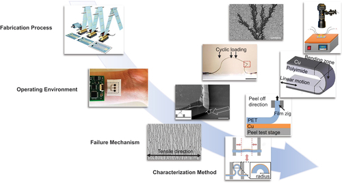
Given their extensive range of practical applications, flexible electronic devices are fabricated through diverse fabrication techniques and are designed to function in varied environmental conditions. This heterogeneity in fabrication and functionality results in distinctive failure modes throughout their service lifetimes. These failure modes can be broadly categorized into four classes: strength, fatigue, interfacial, and electrical failure, as depicted in . These modes significantly affect their long-term utility in crucial sectors such as engineering and biomedical sciences. Noteworthy studies have been undertaken to investigate the failure mechanisms of flexible electronics, ranging from analytical models to numerical methods and advanced characterization methods. As a result, it is vital to closely examine the latest advancements in various failure modes of flexible electronic devices to enhance our understanding of these failure mechanisms.
Figure 1. Overview of failure of flexible electronic devices from perspective of failure mode, characterization methods, fabrication process and operating environment. Strength failure: Adapted with permission. Copyright 2010, Elsevier BV [Citation40]. Interfacial failure: Adapted with permission. Copyright 2014, Elsevier BV [Citation41]. Fatigue failure: Adapted with permission. Copyright 2021, Wiley-VCH Verlag [Citation42]. Electrical failure: Reproduced with permission. Copyright 2022, American chemical Society [Citation43]. Bending strength test: Adapted with permission. Copyright 2018, Elsevier BV [Citation44]. Peel-off test. Adapted with permission. Copyright 2018, Elsevier BV [Citation44]. Laser-induced interfacial spallation. Adapted with permission. Copyright 2020, American chemical Society [Citation45]. Bending fatigue test. Adapted with permission. Copyright 2013, Elsevier BV [Citation46]. Tensile fatigue test. Adapted with permission. Copyright 2022, Nature Publishing group [Citation47]. Electromigration test. Adapted with permission. Copyright 2019, Springer Verlag [Citation48].
![Figure 1. Overview of failure of flexible electronic devices from perspective of failure mode, characterization methods, fabrication process and operating environment. Strength failure: Adapted with permission. Copyright 2010, Elsevier BV [Citation40]. Interfacial failure: Adapted with permission. Copyright 2014, Elsevier BV [Citation41]. Fatigue failure: Adapted with permission. Copyright 2021, Wiley-VCH Verlag [Citation42]. Electrical failure: Reproduced with permission. Copyright 2022, American chemical Society [Citation43]. Bending strength test: Adapted with permission. Copyright 2018, Elsevier BV [Citation44]. Peel-off test. Adapted with permission. Copyright 2018, Elsevier BV [Citation44]. Laser-induced interfacial spallation. Adapted with permission. Copyright 2020, American chemical Society [Citation45]. Bending fatigue test. Adapted with permission. Copyright 2013, Elsevier BV [Citation46]. Tensile fatigue test. Adapted with permission. Copyright 2022, Nature Publishing group [Citation47]. Electromigration test. Adapted with permission. Copyright 2019, Springer Verlag [Citation48].](/cms/asset/2c9d8bbd-8220-47da-a0bf-f760e7ecbd96/tsnm_a_2261775_f0001_c.jpg)
In this study, we present an exhaustive review of these four failure modes in flexible electronics, concentrating on their respective failure mechanisms and characterization methods. This review begin with an overview of the triggers of device failure, namely, the fabrication process and operating environment, followed by an in-depth discussion of the failure mechanisms concerning strength, fatigue, interfacial, and electrical failure, which are detailed in Sections 3 to 7. We conclude by presenting a perspective on the prevalent challenges and prospective avenues for future research.
2. The influence of fabrication processes and operating environments
The multistage fabrication process coupled with diverse operating environments present potential risks to flexible electronic devices. This section delves into the negative impacts of these fabrication processes and operating environments on the stability of flexible electronic devices.
2.1. Fabrication processes
The standard fabrication techniques () for flexible electronic devices include photolithography, soft lithography, inkjet printing, transfer printing, encapsulation technology, and mechanically guided assembly. These techniques are described in detail below.
Figure 2. Schematic illustration of representative fabrication process for flexible electronic devices. (a) Photolithography process. Adapted with permission. Copyright 2016, Elsevier BV [Citation49]. (b) roll-to-roll printing. Reproduced with permission. Copyright 2018, American chemical Society [Citation50]. (c) deterministic assembly. Adapted with permission. Copyright 2021, Wiley-VCH Verlag [Citation51]. (d) inkjet printing process. Adapted with permission. Copyright 2018, American chemical Society [Citation52]. (e) mechanically guided 3D assembly of a resistive vibration sensor. Adapted with permission. Copyright 2021, Wiley-VCH Verlag [Citation42]. (f) encapsulation of a flexible microfluidic electronic system. Adapted with permission. Copyright 2014, American Association for the Advancement of Science [Citation53].
![Figure 2. Schematic illustration of representative fabrication process for flexible electronic devices. (a) Photolithography process. Adapted with permission. Copyright 2016, Elsevier BV [Citation49]. (b) roll-to-roll printing. Reproduced with permission. Copyright 2018, American chemical Society [Citation50]. (c) deterministic assembly. Adapted with permission. Copyright 2021, Wiley-VCH Verlag [Citation51]. (d) inkjet printing process. Adapted with permission. Copyright 2018, American chemical Society [Citation52]. (e) mechanically guided 3D assembly of a resistive vibration sensor. Adapted with permission. Copyright 2021, Wiley-VCH Verlag [Citation42]. (f) encapsulation of a flexible microfluidic electronic system. Adapted with permission. Copyright 2014, American Association for the Advancement of Science [Citation53].](/cms/asset/91b28536-bd97-44a2-9240-3c1d67b0e5c4/tsnm_a_2261775_f0002_c.jpg)
Photolithography is a predominant technique for producing flexible electronic devices, offering superior resolution. Despite its widespread use in device patterning, its complexity and environmental demands, can be challenging. As depicted in , the process begins with the application of a photoresist to the substrate surface, forming a protective coating. Subsequently, UV light is directed through a mask plate onto the photoresist, triggering a chemical reaction that results in either photodecomposition (for positive photoresists) or photocrosslinking (for negative photoresists). The subsequent development phase involves dissolving the photoresist to either remove the exposed region (positive photoresist) or the unexposed region (negative photoresist), effectively replicating the mask pattern onto the coated substrate. The pattern is then etched onto the substrate to produce the desired design. A notable concern in this fabrication approach is that while the photoresist forms the device’s pattern and the residual etchant eliminates specific material, solvents may persist on the device surfaces. This residual presence can compromise the electrical performance or introduce imperfections in the final products [Citation49].
Roll-to-roll printing, demonstrated in , facilitates the continuous production of flexible, biocompatible electrode arrays on polyethylene-terephthalate (PET) substrates. The procedure involves the deposition of silver, carbon, and insulator ink layers into the grooves of a gravure plate, which are subsequently transferred to a substrate via rotation of a roll or carrier on a roll core [Citation50]. Both the operating temperature and humidity significantly influence the fabrication process. Fluctuating conditions may disrupt ink fluidity and coating uniformity, impacting device quality and stability [Citation22]. Furthermore, insufficient adhesion between the printed material and the substrate could lead to circuit delamination or failure [Citation21].
Transfer printing technology involves the strategic arrangement of micro and nano materials into spatially structured functional modules. It encompasses three primary types: additive transfer, subtractive transfer, and deterministic assembly. In the deterministic assembly, for instance, the structure is transported from the donor substrate to the stamp and finally to the receiver substrate by manipulating the adhesion and fracture mechanisms at the critical ink/receptor interface, as depicted in [Citation51]. The technology’s essence lies in its ability to efficiently and precisely select and arrange functional components for device structure. These components span intricate molecular-scale materials such as self-assembled monolayers, nanotubes, graphene, and functional polymers, to high-performance rigid substances like single-crystalline inorganic semiconductors, metals, and oxide thin films. They also include fully integrated device structures, encompassing thin film transistors (TFTs), light-emitting diodes (LEDs), CMOS circuits, sensing arrays, and solar cells [Citation51]. Despite its benefits, it can experience failures due to insufficient adhesion during production, similar to roll-to-roll printing [Citation54]. The transfer process might also result in uneven substrate surfaces, which can negatively impact circuit quality and stability [Citation55].
Inkjet printing, a non-contact patterning method, facilitates rapid structuring of intricate designs. presents a schematic of this process, encompassing ink ejection, droplet flight, ink-substrate impact, spreading, and drying [Citation52]. The performance of fabricated flexible devices hinges on spray conditions including solvent type, concentration, and substrate surface properties. Ink diffusion from the print head can cause short circuits, impacting electronic lifespan and stability [Citation56]. Moreover, uneven particle size distribution in the ink could cause precipitation, compromising the device’s reliability and stability [Citation57].
Mechanically guided assembly, a versatile method for creating three-dimensional (3D) structures, leverages a prestrained elastomer platform to drive 2D to 3D conversions via buckling () [Citation42]. Nonetheless, this approach poses challenges. Missteps in strain release during fabrication could induce excessive curvature in certain areas, risking localized damage. Furthermore, the assembly process often necessitates interactions across multiple material interfaces. This may provoke interfacial delamination in the bonding area or total structure adhesion, consequently undermining successful 3D formation [Citation58].
Encapsulation technology, as shown in , is vital in fabricating flexible electronic devices, because it selectively prevents or allows the entry of external environmental factors, including water and oxygen, while mitigating the impact of both internal and external heat exchange on device performance [Citation53]. However, it presents certain challenges. For instance, interfacial adhesion can affect the encapsulation quality, and poor adhesion between the encapsulation material and the flexible electronics could result in inadequate protection [Citation59]. The stiffness of the encapsulation material affects the flexibility and bendability of the flexible electronic device. Moreover, disparities in physical properties between materials can introduce various issues [Citation53]. For example, if the thermal expansion coefficients of the encapsulation and substrate materials are mismatched, temperature variations could create stress disparities, leading to device failure.
2.2. Operating environments
Here, we investigates diverse operating environments for flexible devices and systems. Importantly, the categorization of flexible devices in is guided by their distinct usage contexts: epidermal electronics, implantable devices, textile-based systems, and engineering monitoring devices. Each device type encounters distinct challenges within its operating context:
Figure 3. Operating environments of flexible electronic devices and their influencing factors. (a) Epidermal electronics. 1) flexible sensor arrays that can be used for pressure monitoring on human surfaces. Reproduced with permission. Copyright 2016, Nature Publishing group [Citation60]. 2) 3D-printed soft neural probe with nine channels by the conducting polymer ink and the PDMS ink. Reproduced with permission. Copyright 2020, Nature Publishing group [Citation61]. 3) Fractal device structure of the EEG measurement system, where the left image represents the device cascade on the auricle and mastoid, and the right image represents the amplified interconnections. Adapted with permission. Copyright 2015, Proceedings of the National Academy of Sciences [Citation62]. (b) implantable devices. 1) wireless biodegradable sensor wrapped around the femoral artery and secured with sutures. Adapted with permission. Copyright 2019, Nature Publishing group [Citation18]. 2) Implanted pressure sensor in front of the eye model. 3) wireless implanted pressure sensor with an external coil in front of the eye model. Reproduced with permission. Copyright 2008, IEEE [Citation63]. (c) textile-based devices. 1) Solid-state textile-based micro-supercapacitors. 2) the scanning electron microscopy (SEM) image of a solid-state textile- based micro-supercapacitors. Adapted with permission. Copyright 2016, Wiley-VCH Verlag [Citation19]. 3) textile-based pressure sensor. 4) LEDs lit by a DC source through knotted textile conductive circuits. Reproduced with permission. Copyright 2017, Wiley-VCH Verlag [Citation64]. (d) flexible electronic devices in engineering applications. 1) flexible skin for Boundary layer state measurement and flight Attitude Identification on unmanned aerial vehicle (UAV). Reproduced with permission. Copyright 2023, IOP Publishing [Citation13]. 2) schematic diagram of the UAV equipped with smart sensing skin for sensing wind pressure. Adapted with permission. Copyright 2020, Springer Verlag [Citation65].
![Figure 3. Operating environments of flexible electronic devices and their influencing factors. (a) Epidermal electronics. 1) flexible sensor arrays that can be used for pressure monitoring on human surfaces. Reproduced with permission. Copyright 2016, Nature Publishing group [Citation60]. 2) 3D-printed soft neural probe with nine channels by the conducting polymer ink and the PDMS ink. Reproduced with permission. Copyright 2020, Nature Publishing group [Citation61]. 3) Fractal device structure of the EEG measurement system, where the left image represents the device cascade on the auricle and mastoid, and the right image represents the amplified interconnections. Adapted with permission. Copyright 2015, Proceedings of the National Academy of Sciences [Citation62]. (b) implantable devices. 1) wireless biodegradable sensor wrapped around the femoral artery and secured with sutures. Adapted with permission. Copyright 2019, Nature Publishing group [Citation18]. 2) Implanted pressure sensor in front of the eye model. 3) wireless implanted pressure sensor with an external coil in front of the eye model. Reproduced with permission. Copyright 2008, IEEE [Citation63]. (c) textile-based devices. 1) Solid-state textile-based micro-supercapacitors. 2) the scanning electron microscopy (SEM) image of a solid-state textile- based micro-supercapacitors. Adapted with permission. Copyright 2016, Wiley-VCH Verlag [Citation19]. 3) textile-based pressure sensor. 4) LEDs lit by a DC source through knotted textile conductive circuits. Reproduced with permission. Copyright 2017, Wiley-VCH Verlag [Citation64]. (d) flexible electronic devices in engineering applications. 1) flexible skin for Boundary layer state measurement and flight Attitude Identification on unmanned aerial vehicle (UAV). Reproduced with permission. Copyright 2023, IOP Publishing [Citation13]. 2) schematic diagram of the UAV equipped with smart sensing skin for sensing wind pressure. Adapted with permission. Copyright 2020, Springer Verlag [Citation65].](/cms/asset/3507da6f-d7c5-4a54-b77d-235db2897830/tsnm_a_2261775_f0003_c.jpg)
Load: Epidermal electronics experience mechanical loads such as external pressure and impact [Citation60]. Implantable devices within the human body endure biological loads like bodily fluid pressure, and muscular contractions [Citation18]. Textile-integrated devices must withstand mechanical stresses like clothing friction and pulling [Citation19]. These loads may cause deformation and damage to the devices.
Humidity Change: Fluctuating internal and external humidity levels can destabilize and compromise the reliability of flexible electronic components. High humidity can lead to water absorption by device materials, resulting in short circuits or component failure [Citation66]. In addition, Humidity changes can also weaken flexible electronics adhesion, causing delamination or deformation [Citation67].
Temperature Variation: Devices, whether on the surface or inside the body, are influenced by ambient temperature changes, potentially causing shape alterations and performance instability. For example, high temperatures might trigger material thermal expansion, impacting the device’s form and characteristics [Citation68].
Chemical Substances: Chemicals present in the human body may affect implantable flexible devices’ materials and components [Citation69]. Epidermal electronics may be influenced by sweat, sebum, and other substances [Citation70], causing corrosion, oxidation, and potentially, device failure.
Light Exposure: Devices exposed to the natural environment are susceptible to light effects. Sustained UV light exposure may cause material aging, deterioration, or deformation in flexible electronics [Citation71].
Extreme environments: Flexible sensors deployed in engineering applications often encounter severe conditions. For instance, flexible electronics used on aircraft skin need to endure extreme temperature changes, wing vibrations during high-speed flight [Citation23,Citation72,Citation73], and interference from aircraft radar radio frequency radiation [Citation74]
In summary, unfavorable factors during manufacturing can lead to device defects and potential failure, while adverse operational conditions can directly or indirectly impair device performance and stability. Therefore, when designing and manufacturing flexible electronic devices, it’s crucial to account for these potential failure mechanisms and apply corresponding characterization methods. This ensures device stability, reliability, and safe operation within their intended environments
3. Strength failure
In flexible electronics, conductive materials such as metal-based materials [Citation75–78], carbon-based materials [Citation75,Citation79,Citation80], and conductive polymers [Citation81–86]), along with semiconductors including semiconducting NWs [Citation87,Citation88], semiconducting organics [Citation86,Citation89–91], light-absorbing semiconductors [Citation92–94], field-effect transistors [Citation75,Citation79]) serve as functional components. Elastomeric polymers like PDMS [Citation95–97], PI [Citation98,Citation99], PET [Citation20,Citation100], PEN [Citation101], PES [Citation102], PGS [Citation103], PAR [Citation26] form the flexible platform. As these electronics are fabricated from thin films of flexible and stretchable materials, they present unique properties and damage mechanisms under force, distinct from traditional rigid electronics [Citation104]. Various strength failure modes can occur, with the characteristics influenced by the choice of materials and their structures [Citation105–108]. This section will discuss strength failure modes, including tension, bending, and impact-induced damage, as well as damage from mismatched material properties in multi-layer structures.
3.1. Tensile-induced damage
The durability of flexible electronics under intense tensile loading is significantly influenced by the formation and propagation of cracks [Citation109,Citation110]. Such cracks typically develop and expand gradually to relieve considerable localized stress [Citation111,Citation112]. Consider a uniaxial tensile test () as an example: a brittle film on a flexible substrate typically experiences three stages as the tensile strain escalates. Initially, cracking begins at the critical strain; this is followed by the onset of midpoint cracking and transverse fragment buckling as the strain increases; finally, once a certain strain threshold is surpassed, no additional cracks form, marking the achievement of saturation crack density [Citation109]. However, the load-bearing capacity of brittle layers is inherently constrained by their functional and material characteristics, typically resulting in the appearance of cracks within functional layers prior to substrate failure [Citation117,Citation118]. Consequently, the brittle film invariably fractures at a strain lower than the flexible polymer substrate. Instances of such systems with low fracture strains encompass chromium on polydimethylsiloxane (<1%) [Citation119], silica on polyethylene terephthalate (<3%) [Citation28], tantalum on polydimethylsiloxane (<0.5%) [Citation120] and titanium oxide/carbon nanofibers on polyacrylonitrile/polyvinyl pyrrolidone (<1.5%) [Citation121].
Figure 4. Strength failure mechanisms. (a) illustration of the three stages of brittle film fragmentation under uniaxial loading; the insets show the progression of cracks of a 20 nm thick SiOx coating on a 12 μm thick PET substrate. Adapted with permission. Copyright 2002, Elsevier BV [Citation109]. (b) Demonstration of the failure of a flexible accelerometer upon impact. Adapted with permission. Copyright 2014, Elsevier BV [Citation113]. (c) analytical model of stretchable electronic devices with viscoelastic packages and soft substrates subjected to impact loads on the surface of human skin. Adapted with permission. Copyright 2016, ASME [Citation114]. (d) flexible microfluidic electronic systems under stretch and twist configurations. Adapted with permission. Copyright 2014, American Association for the Advancement of Science [Citation53]. (e) left, schematic illustration of a flexible sensor with a non-bonded interface, exhibiting a notable mechanical mismatch between the layers. Right, SEM image of the sensor in its bent state, highlighting stable bonding between the microcones and the dielectric layers. Adapted with permission. Copyright 2022, Nature Publishing group [Citation115]. (f) left, SEM image of the cross-section of an organic–inorganic multilayer permeation barrier. Right, the evolution of defects: beginning as pin-holes, escalating to channel cracks, and culminating in the delamination of the oxide-organic interface. Adapted with permission. Copyright 2010, Elsevier BV [Citation116].
![Figure 4. Strength failure mechanisms. (a) illustration of the three stages of brittle film fragmentation under uniaxial loading; the insets show the progression of cracks of a 20 nm thick SiOx coating on a 12 μm thick PET substrate. Adapted with permission. Copyright 2002, Elsevier BV [Citation109]. (b) Demonstration of the failure of a flexible accelerometer upon impact. Adapted with permission. Copyright 2014, Elsevier BV [Citation113]. (c) analytical model of stretchable electronic devices with viscoelastic packages and soft substrates subjected to impact loads on the surface of human skin. Adapted with permission. Copyright 2016, ASME [Citation114]. (d) flexible microfluidic electronic systems under stretch and twist configurations. Adapted with permission. Copyright 2014, American Association for the Advancement of Science [Citation53]. (e) left, schematic illustration of a flexible sensor with a non-bonded interface, exhibiting a notable mechanical mismatch between the layers. Right, SEM image of the sensor in its bent state, highlighting stable bonding between the microcones and the dielectric layers. Adapted with permission. Copyright 2022, Nature Publishing group [Citation115]. (f) left, SEM image of the cross-section of an organic–inorganic multilayer permeation barrier. Right, the evolution of defects: beginning as pin-holes, escalating to channel cracks, and culminating in the delamination of the oxide-organic interface. Adapted with permission. Copyright 2010, Elsevier BV [Citation116].](/cms/asset/fe06cc86-c2bb-4636-9b85-0f29e00dc82b/tsnm_a_2261775_f0004_c.jpg)
Progressive damage in flexible thin-film devices under tensile loading, as numerous studies indicate, arises predominantly from the differing mechanical properties of the conductive metal film and its flexible polymer substrate (). George et al. examined the crack propagation in metal films on flexible polymer substrates using in-situ atomic force microscopy (AFM) and finite element stress calculations. They categorized damage mechanisms during the tensile test into two phases: initial sprouting and random development of cracks forming a network across the film, followed by depth-oriented development of cracks at maximum stress within the multilayer structure [Citation122]. Heinrich et al. and Stephan Frank et al. conducted in-situ tests on the fragmentation and buckling of thin coating layers on elastomeric substrates. They found that tensile loading caused a mismatch in elastic deformation between the coating and substrate due to different Poisson’s ratios. This induced significant compressive stresses, leading to film bending, continuous delamination, and extensive system damage. They also noted that orthogonal tensile strain allowed for controlled induction of parallel cracking [Citation123]. M.J. Cordill et al. quantified the Poisson effect on thin film structures under tensile load, illustrating the sequence of film cracking in tension: initial perpendicular cracks form a single crack band, followed by bending in the same direction, growth of the bent section, and cracking at the apex [Citation43].
The failure of flexible films under tensile loading is primarily determined by the crack onset strains (COS) [Citation109,Citation124], which denote the strain at initial crack detection. Two analytical methods, the weakest link and shear lag models, have been instrumental in related studies. The former considers fracture toughness is determined by the most brittle region (‘weakest link’) along the crack front [Citation124,Citation125], whereas the latter the shear stress is proportional to the relative displacement of the flexible substrate to the metal layer [Citation126,Citation127].
Utilizing the weakest link model, Y. Leterrier et al. [Citation124] proposed a crack initiation strain model based on fragmentation tests on uniaxial silicon oxide-coated polyethylene terephthalate (PET) films. This model identifies the strength distribution of a coating fragment under stress , characterized by length
, width
and thickness
, using the equation:
where and
represent the distribution of flaws within the functional layer’s volume and on its surface, respectively. Moreover, Assuming the initial fracture as a random event, the crack onset strains are dependent on the coating’s surface area, and the average fracture strain are calculated by
where ,
and
represent strength distribution parameters derived from the early linear extrapolation of partial experimental results,
signifies the film portion’s length being inspected for the first crack,
denotes the functional layer’s modulus of elasticity, and
and
are normalizing factors,
represents the gamma function.
The shear lag model provides an additional analytical method to compute stress redistribution [Citation127]. Upon applying the energy release rate relationship derived from Laws and Dvorak’s work to the functional layer-substrate system (assuming residual stresses are negligible), the crack initiation strain can be determined by [Citation128,Citation129]:
where ,
,
and
represent the fracture toughness of the functional layer, the elastic modulus of the substrate, functional layer, and the entire film, respectively, while
and
indicate their corresponding thickness.
Several studies have leveraged these principles to enhance the COS of brittle metal films supported by flexible polymers. Tanja Jörg et al. studied the deformation behavior of 40–500 nm thick sputter-deposited Mo films, correlating fracture strength and COS with decreasing film thickness [Citation130]. They also assessed the impact of deposition conditions on the structure-stress relationship, establishing that residual stress tailoring can reduce the COS [Citation131]. Similarly, M.J. Cordill et al. investigated fracture, flexure, and delamination of Cr films on polyimide (PI) under tensile strain using the shear hysteresis model. Their findings suggest that film fracture and delamination are thickness-dependent and a thinner film with high crack density may be less reliable than a thicker adherent layer [Citation132,Citation133]. Furthermore, V.M. Marx et al. explored the strain-induced phase transition in two-phase Co films on PI, concluding that the strain-induced phase transition can enhance the ductility of cobalt films, thereby delaying the onset of cracking [Citation134].
Efforts have been made to delay the onset of cracking in rigid films on flexible substrates under tension through microstructural optimization of the rigid films themselves. Inhwa Lee et al. improved the weak cracking resistance of flexible nanoparticle films by integrating very long nanowires, demonstrating that nanowires longer than 90 μm inhibit the overall film cracking and significantly reduce resistivity [Citation135]. Impressive mechanical properties under tensile and compressive bending were displayed by a novel nanocomposite of nanowire-reinforced nanoparticle matrix film developed by Young D. Suh et al., offering an inspired alternative for flexible and transparent electrode applications [Citation136]. Furthermore, Chullhee Cho et al. fabricated durable thin-film electrodes by implanting an ultra-thin interlayer (graphene, molybdenum disulfide, or hexagonal boron nitride) between a metal film and a flexible substrate, thereby increasing the allowable strain before electrical failure by 400% [Citation137].
Under tensile loading, flexible films doped with nanomaterials exhibit a distinctive failure mechanism. Nanoparticle-coated flexible films display a pattern of crack development analogous to that of individual metallic films under tensile load. Sanghyeok Kim et al.‘s exploration of Ag nanoparticle (Ag NP) films on flexible substrates showed that with increasing tensile strain, cracks develop perpendicular to the tensile load and grow along Ag NP grain boundaries [Citation138]. This aligns with past studies on crack extension in nanocrystalline metal films [Citation139].
3.2. Bending-induced damage
In flexible devices, unavoidable operation under bending conditions can significantly affect performance and reliability. Brittle materials within these devices are susceptible to stress concentration during bending, often leading to rupture [Citation140]. This damage mechanism can also manifest at interconnects [Citation141]. Further, bending stresses can deform or destabilize features like micro-bending structures and three-dimensional elements in flexible electronic devices, compromising their performance [Citation42].
Structures subjected to bending loads experience two distinct stress states: tensile stresses on convex surfaces and compressive stresses on concave ones [Citation142,Citation143]. The relative position of the brittle structure to the flexible polymer substrate dictates two potential failure modes under flexural loading. Under tension, channel cracking of the film occurs, similar to the damage under tensile stress. Conversely, under compression, the functional layer might experience tunnel buckling, delamination, and cracking [Citation144]. Contrary to the effects of uniaxial stretching, flexible devices undergoing bending deformation do not experience failures from coupled compressive and tensile stress. Such combined stresses typically result in a sequence of film cracking, buckling, and eventually delamination.
The location of the neutral plane, the dividing line between compression and tension, is of significant importance. The ‘plane sections remain plane’ assumption yields an analytical solution for the neutral plane location as follows [Citation145]:
where represents the neutral plane axis location,
the material’s modulus of elasticity,
the layer thickness, and
the layer index. This equation suggests that a similar thickness of the encapsulation layer and the polyimide substrate can counteract the mechanical strain applied to the functional layer [Citation146].
Nonetheless, the classical beam theory ceases to be applicable in cases with a substantial difference in elasticity modulus between layers. When a flexible layer with a small modulus of elasticity is sandwiched between two stiff layers, the central soft layer undergoes significant shear deformation during bending, decoupling the deformations of the top and bottom stiff layers [Citation147]. Consequently, the entire multilayer structure has multiple zero-stress surfaces; each stiff layer has its neutral axis and bending center. Lan Li et al. analytically determined these neutral axis locations during the design and fabrication of a flexible, high-refractive-index contrast 3D photonic device [Citation148].
Determining the neutral plane proves instrumental in optimizing flexible device design under bending loads. Seung-Yoon Kim et al. utilized analytical and numerical simulations to position the neutral mechanical plane (NMP) optimally, achieving high-performing mechanically flexible silicon nanomembranes (NMs) completely depleted of silicon field-effect transistors on an insulator. The device demonstrated robust mechanical and electrical stability even under a 1 mm bending radius [Citation149]. Sangmin Lee et al. proposed a design rule – neutral axis (NA) engineering – that controls the neutral plane’s position using a buffer layer on the ITO layer, improving the bendability of organic solar cells to a bending radius of approximately 1 mm [Citation150]. Recognizing flexible displays often comprise several thin films with varied thicknesses and linear elastic mechanical properties, Chang-Chun Lee et al. proposed an analytical solution for bending stress/strain in multilayer thin-film flexible displays. They estimated specific outcomes for alternating layered systems, revealing core trends in the normalized bending strain and neutral axis position’s dependence on the modulus and thickness ratio of relevant layers [Citation151].
Flexible films doped with nanowires exhibit a distinct destruction process under bending deformation. The failure criterion of silver nanowire (Ag NW) electrodes on polymer substrates in flexible devices was proposed by Donggyun Kim et al., using in-situ mechanical tests on individual Ag NWs. The findings reveal that Ag NW electrodes undergo strain-dependent electrical failures linked to unique deformation properties and the size-dependent brittle-ductile transition of the fivefold twinned Ag NWs. All Ag NWs above 40 nm in diameter display brittle fracture, with consistent stress-strain responses, regardless of size. Conversely, Ag NWs beneath 40 nm in diameter show increased strain- at-break figures, with smaller diameters correlating with higher ductility and enhanced deformability in subsequent flexible electrodes. Additional in-situ tensile tests demonstrated that Ag NWs exceeding 40 nm in diameter experience brittle fracture at roughly 2.6% lattice strain due to localized necking, potentially causing the steep resistance increase in flexible electrodes under bending pressure. Therefore, the fracture threshold for bending-induced failure in conductive electrode films is premised on the lattice strain of Ag NWs, which triggers brittle fracture, resulting in an evident size effect [Citation141].
Flexible electronic devices often experience performance alterations due to bending strain prior to outright failure. Liu et al. studied this using a flexible single-crystal silicon p-eigen-n diode, finding that bending-induced physical deformation leads to misalignment of electrodes and the intrinsic region. This reduces the effective horizontal electric field, thereby decreasing the diode’s current density, with the effect amplifying as bending strain increases [Citation152]. In a similar vein, Yang et al. explored the physical mechanisms of flexible microwave passive components under mechanical bending. Their findings revealed a direct relationship between a decreasing bending radius and increasing inductance and capacitance values of the component [Citation153].
3.3. Impact-induced damage
Flexible engineering devices, epidermal devices, and textile-based devices are prone to unexpected impacts or collisions, potentially leading to device failure () [Citation154–158]. Notably, a trade-off exists between mechanical robustness and functional performance in flexible electronics like e-skins. Enhancements in resilience to external mechanical shocks often compromise their sensing capabilities, monitoring functionality, flexibility, and stretchability [Citation159,Citation160].
Advances have been made in designing impact-resistant devices. J. H. Yuan et al. introduced a viscoelastic encapsulation layer atop a stretchable electronic device to counter impact loads and diffuse energy through viscoelastic properties. Their theoretical model () suggests that the impact resistance of such devices depends on the encapsulation layer’s thickness and viscoelastic attributes, as well as the impact’s duration [Citation114]. Yanan Wang et al. engineered a Mechanical Shock Tolerant (MST) e-skin that spontaneously replicates the protective and sensory functions of natural skin. This e-skin, comprising a Conductive Collagen Fiber Sponge (CFS) enveloped in an Elastic Non-Newtonian Gel (ENG), efficiently dissipates mechanical energy when subject to impact load, leading to a 455% extension in buffer time and a 76.5% decrease in peak force [Citation161].
3.4. Destruction caused by the mismatch of material properties of multi-layer structures
Flexible electronic devices often utilize multilayer structures to maintain diverse functionalities such as monitoring, stretchability, and hermeticity [Citation162–164]. Nevertheless, these structures can present drawbacks, primarily due to the distinct physical properties of different layers. For instance, the modulus of elasticity can differ up to five orders of magnitude between layers [Citation115,Citation165–169], and materials can have varied sensitivities to humidity and temperature fluctuations [Citation170–172]. Thus, interface disruption or delamination may occur under complex mechanical deformation or environmental changes.
Even without external changes, flexible devices may degrade or fail due to the mismatch in physical properties within their multilayer materials. Given the stringent encapsulation requirements of these devices, any mechanical defects in the brittle oxide film within the multilayer structure can severely impact performance. While the polymer layers in these structures can recover from large strains, the metal oxide layers are brittle and can fracture under minor strains from internal hygroscopic expansion. Typical fracture modes include oxide layer channel cracking and delamination at the oxide-organic interface. Moisture mainly penetrates the structure through pinhole-like defects in the oxide layer [Citation173,Citation174]. However, channel cracks can exacerbate moisture penetration by providing a line source rather than a point source from the initial pinhole. When delamination at the oxide-organic interface is accompanied by channel crack expansion and increased hygroscopic expansion, the situation worsens [Citation66,Citation175]. Moisture absorption at the delamination interface creates a regional moisture source, significantly accelerating humidity penetration into the multilayer structure, which can be fatal for the flexible device [Citation116].
3.5. Characterization methods and experiments for strength failure
Strength failure characterization methods, their corresponding procedures, and instruments are detailed in . Notably, we currently lack characterization methods for destruction caused by material property mismatches in multi-layer structures.
Table 1. Characterization methods of strength failure.
To assess the failure mechanism of flexible electronic devices under tensile loading, electromechanical test methods, such as uniaxial tensile or fragmentation testing, are used (). This method is employed for new material and deposition process investigations in flexible electronic device development [Citation180,Citation181], and also for flexible thin film device inspection [Citation180–182]. In these tests, the film-substrate system undergoes strain, forming cracks perpendicular to the strain direction until crack spacing saturates [Citation129]. The critical reliability parameter, crack onset strain (COS), is maintained below any mechanical strain experienced during fabrication or use. To rapidly and accurately measure characterization data like COS, tensile testing is often paired with in-situ monitoring techniques for crack detection and mechanical characterization. Common techniques include optical microscopy (OM) [Citation183–185], atomic force microscope (AFM) [Citation132,Citation186,Citation187], scanning electron microscope (SEM), and field emission scanning electron microscope (FESEM) [Citation188–191]. In-situ X-ray diffraction (XRD) is also used to determine thin film deformation mechanisms [Citation188,Citation189,Citation192,Citation193]. Characterization of electrical properties is also crucial in tensile testing. Pre-established metal contacts can measure the resistance of the thin film structure [Citation110,Citation194–196]. Resistivity changes pre- and posttest help ascertain the impact on device performance or possible failure.
Figure 5. Characterization methods for strength failure. (a) SEM images of Mo films of varying thickness - (I) 500 nm, (II) 250 nm, (III) 70 nm, and (Ⅳ) 40 nm - on PI substrates after the application of a 12% strain. Adapted with permission. Copyright 2017, Elsevier BV [Citation130]. (b) the falling ball test, employed to evaluate the reliability of pressure stress concentrations in flexible displays. Left, a fully supported sample backed by a solid steel block. Right, a partially supported sample propped on two rollers. Reproduced with permission. Copyright 2008, IEEE [Citation176]. (c) static bending test of the CIF assembly, utilizing bending rods of varied radii. Adapted with permission. Copyright 2016, IEEE [Citation177]. (d) three-point static bending test. Reproduced with permission. Copyright 2016, IEEE [Citation177]. (e) the lab-made bending test machine and outer/inner bending test experiments. Reproduced with permission. Copyright 2014, Elsevier BV [Citation178]. (f) optical device for strain measurement on the surface of a curved film. Adapted with permission. Copyright 2021, Wiley-VCH Verlag [Citation179].
![Figure 5. Characterization methods for strength failure. (a) SEM images of Mo films of varying thickness - (I) 500 nm, (II) 250 nm, (III) 70 nm, and (Ⅳ) 40 nm - on PI substrates after the application of a 12% strain. Adapted with permission. Copyright 2017, Elsevier BV [Citation130]. (b) the falling ball test, employed to evaluate the reliability of pressure stress concentrations in flexible displays. Left, a fully supported sample backed by a solid steel block. Right, a partially supported sample propped on two rollers. Reproduced with permission. Copyright 2008, IEEE [Citation176]. (c) static bending test of the CIF assembly, utilizing bending rods of varied radii. Adapted with permission. Copyright 2016, IEEE [Citation177]. (d) three-point static bending test. Reproduced with permission. Copyright 2016, IEEE [Citation177]. (e) the lab-made bending test machine and outer/inner bending test experiments. Reproduced with permission. Copyright 2014, Elsevier BV [Citation178]. (f) optical device for strain measurement on the surface of a curved film. Adapted with permission. Copyright 2021, Wiley-VCH Verlag [Citation179].](/cms/asset/0e3f123d-df2c-4acb-8cc0-1da7af65e52f/tsnm_a_2261775_f0005_c.jpg)
Several bending experiments and monitoring techniques have been devised to evaluate the electromechanical performance of flexible devices under bending deformation. One such method, the rod bending test (), mounts flexible devices on cylindrical fixtures with different radii to calculate strain; concurrent in-situ electrical property tests are also performed [Citation152,Citation153,Citation197]. Ji-Hye Kim et al. expanded on this with a three-point bending test () to quantify the load and bending radius at the fragment fracture in chip-in-flex (CIF) [Citation177]. Yang et al. employed a custom bending test apparatus () to evaluate flexible devices bidirectionally. Starting with a flat-clamped sample, the decreasing bending radius was achieved by moving the fixtures closer. The outer bending (‘Λ’) induces tensile stresses on the film, while the inner bending (‘V’) results in compressive stresses [Citation178]. Common techniques for monitoring the bending properties of flexible device layers include the direct encapsulation of strain-sensitive functional layers with the aid of existing bending devices [Citation198–200], and the installation of flexible strain sensors on device surfaces [Citation201]. However, strain measurements can be significantly skewed by neutral axis shifts, interlayer interface sliding, and the effects of strain sensors or strain-sensitive layers [Citation202]. Hence, the use of alternative methods to observe the curvature and surface strain of curved films is vital in the research and development of flexible device. Kohei Kuwahara et al. evaluated the curvature at the bent film’s center using a charge-coupled device (CCD) camera to capture the film shape profile [Citation184,Citation185]. Norihisa Akamatsu et al. employed a surface marking grating method for quantitative evaluation of flexible materials’ surface radius () [Citation203,Citation204]. Various other non-electrical methods for measuring curvature and surface strain have been reported, including photoelasticity, Moiré patterns, and X-ray diffraction [Citation179,Citation205,Citation206]. Most tests focus on surface strains, with neutral mechanical plane (NMP) or neutral axis (NA) position control typically relying on theoretical methods. Notably, Masayuki Kishino et al. first experimentally quantified the internal strain distribution of bent PDMS films using a cholesteric liquid crystal elastomer (CLCE) as an internal strain sensor, determining the NMP position [Citation207].
There are fewer studies on mechanical characterization tests for flexible electronic devices’ impact resistance. Yanan Wang et al. proposed an effective method for designing mechanically shock-tolerable (MST) e-skins, utilizing a drop hammer impact tester to evaluate the samples’ mechanical impact resistance. For control, the base itself was subjected to direct drop hammer impacts [Citation161]. Alternatively, Quayle Chen et al. tested flexible displays’ drop resistance with a ball drop test. Two extreme support conditions were considered: ‘full support,’ where a solid steel block supports the sample, and ‘partial support,’ where two rollers support it (). A steel ball is dropped from a fixed height above the sample, creating an impact load and causing stress concentration on its surface. The drop height is altered until the sample is destroyed. To enhance drop point precision, a magnetically controlled system is typically employed to minimize experimenter interference [Citation176].
4. Interfacial failure
The integration of semiconductor or metal conductors with a flexible substrate results in unique characteristics. Notably, the substrate, being a flexible material, has a significantly lower modulus of elasticity than the rigid functional layer. Consequently, the soft interface between the film and substrate introduces novel attributes of structural damage. Park et al. [Citation208] observed a system consisting of single-crystal silicon strips and rods supported by plastic sheets through a compression bending experiment, during which one end of the substrate was fixed, and the other end of the substrate was compressed to cause upward buckling instability of the substrate until failure occurred between the thin film structure and the flexible substrate. The results indicated a variation in damage patterns based on film thickness. With a thin film, bending-induced failure was dominant, characterized by strain values surpassing the failure threshold due to bending, causing film fracture. A thicker film altered the damage mode to interface slipping, which prevented cracking even under high loads. Further increasing film thickness led to delamination as the dominant mode, starting at the strip edge and progressing to the center with increased bending, leading to eventual film detachment.
4.1. Interfacial slipping
Interface slipping, observable through in-situ tests, evolves gradually as tensile strain increases, as shown in [Citation209]. In devices under tensile strain, this slipping commonly precedes material fracture. Park et al.‘s findings suggest that interfacial slip,
although difficult to observe, poses a greater risk than material fracture in practical applications [Citation208]. In the context of linear-elastic fracture mechanics (LEFM), the stress intensity factor, , of sliding mode (mode II crack) governs the interfacial slip damage [Citation24,Citation212,Citation213].
Figure 6. Interfacial failure mechanisms alongside their characterization methods. (a) in situ SEM images capturing the progressive sliding at the interface of a horseshoe-shaped copper interconnect deposited on PDMS, stretched sequentially to 30%, 50%, and 100%. Adapted with permission. Copyright 2011, IOP Publishing [Citation209]. (b) delamination between PI layers of prototype stretchable interconnect. (1) SEM image of a bonded sample where PI has been printed once on the top and bottom layers of encapsulated silver, following cooling from curing temperature to ambient temperature. (2) SEM image of a delaminated sample with PI printed three times on the top and bottom layers of encapsulated silver, following cooling from curing temperature to ambient temperature. (3) optical image of a printed interconnect, showcasing variable silver width and PI thickness after cooling from curing temperature to room temperature. Adapted with permission. Copyright 2021, Elsevier BV [Citation210]. (c) the 3M tape adhesion test on the Cu/PET interface, following plasma treatments for durations of 0 min (left) and 7 min (Right). Reproduced with permission. Copyright 2017, Elsevier BV [Citation44]. (d) Scotch tape adhesion test for an al feature on a magazine paper substrate. Reproduced with permission. Copyright 2012, American chemical Society [Citation211]. (e) a peel test device integrated with a camera for examining the local geometry of the delamination front. Adapted with permission. Copyright 2010, IOP Publishing [Citation209]. (f) schematic illustration of T-peel test on Cu/PET flexible substrate. Adapted with permission. Copyright 2017, Elsevier BV [Citation44]. (g) schematic illustration of the laser-induced interplanar sputtering (LIIS) process, employed to facilitate the delamination of PI film from its substrate. Adapted with permission. Copyright 2020, American chemical Society [Citation45].
![Figure 6. Interfacial failure mechanisms alongside their characterization methods. (a) in situ SEM images capturing the progressive sliding at the interface of a horseshoe-shaped copper interconnect deposited on PDMS, stretched sequentially to 30%, 50%, and 100%. Adapted with permission. Copyright 2011, IOP Publishing [Citation209]. (b) delamination between PI layers of prototype stretchable interconnect. (1) SEM image of a bonded sample where PI has been printed once on the top and bottom layers of encapsulated silver, following cooling from curing temperature to ambient temperature. (2) SEM image of a delaminated sample with PI printed three times on the top and bottom layers of encapsulated silver, following cooling from curing temperature to ambient temperature. (3) optical image of a printed interconnect, showcasing variable silver width and PI thickness after cooling from curing temperature to room temperature. Adapted with permission. Copyright 2021, Elsevier BV [Citation210]. (c) the 3M tape adhesion test on the Cu/PET interface, following plasma treatments for durations of 0 min (left) and 7 min (Right). Reproduced with permission. Copyright 2017, Elsevier BV [Citation44]. (d) Scotch tape adhesion test for an al feature on a magazine paper substrate. Reproduced with permission. Copyright 2012, American chemical Society [Citation211]. (e) a peel test device integrated with a camera for examining the local geometry of the delamination front. Adapted with permission. Copyright 2010, IOP Publishing [Citation209]. (f) schematic illustration of T-peel test on Cu/PET flexible substrate. Adapted with permission. Copyright 2017, Elsevier BV [Citation44]. (g) schematic illustration of the laser-induced interplanar sputtering (LIIS) process, employed to facilitate the delamination of PI film from its substrate. Adapted with permission. Copyright 2020, American chemical Society [Citation45].](/cms/asset/80c681aa-7c4c-40c1-bd26-f0dfbfbf6003/tsnm_a_2261775_f0006_c.jpg)
Longchao Dai et al. [Citation214] leveraged fracture mechanics to develop a slip model resistant to delamination damage. Noting the strain energy discrepancy in the structure ahead and behind crack tips [Citation24], they expressed the energy release rate at the film-substrate interface as:
where represents the internal force aligned with the film structure direction, and
denotes the bulking amplitude [Citation208]. Oher parameters (
) aredefined in terms of
(the moduli ratio of the films to the substrate), and
(the thickness ratio of the films to the substrate). They further defined the stress intensity factor for mode II cracks as:
where is the Dundurs’ parameter,
, and
is the phase angle, influenced by material parameters and structural geometry [Citation213]. By substituting the observed
into these equations, they obtained the critical energy release rate and the critical interfacial toughness
. Subsequently, they analyzed the stress state near the crack tip for different film thicknesses during interfacial slip crack expansion. Using the simulated phase angle, they derived the stress intensity factor at the crack tip, which was then compared with the corresponding interfacial toughness.
On this basis, Chen Hang et al. deduced several qualitative conclusions through theoretical modeling and experiments. With an increasing applied load, the film initially slips to dissipate some deformation energy. As the sliding portion expands, the remaining deformation energy surpasses the critical threshold, triggering delamination. This shift from slip to delamination corresponds to the total release of the film’s deformation energy due to delamination [Citation215]. Slip failure, which causes tangential displacement between the film and the substrate, is akin to mode II cracking, while film delamination resembles mode I cracking, where the crack opens. Different crack modes yield distinct stress intensity factors [Citation216]. Therefore, for such flexible devices, which consist of brittle functional layers on flexible substrates and undergo finite deformation, the distinct dimensions and failure modes introduce difficulties and uncertainties concerning interfacial toughness. To address these uncertainties, Hang et al. proposed a slip zone model. By integrating the ideal elastic-plastic cohesive constitutive relation with strength theory, they quantitatively clarified the interfacial slipping failure mechanism in such flexible thin film structures with varying dimensions. They linked failure modes to stress thresholds at the interface, demonstrating that interfacial sliding happens when maximum shear stress equals the interface’s shear strength, and delamination occurs when maximum peeling stress meets the interface’s tensile strength [Citation41].
Interfacial sliding signifies that flexible electronic device failure is not solely governed by the inorganic electronic material’s fracture strain. Rather, it’s also shaped by interfacial shear stresses prompting slip behavior, and these stresses typically peak near the free edge of the functional layer, a finding corroborated by Qian Zhao et al’s experiments [Citation217].
4.2. Interfacial delamination
In thin film structures bending experiments, interfacial delamination is precipitated by interfacial normal stress or peeling stress [Citation208]. Delamination occurs when this stress surpasses the interface’s tensile strength [Citation218,Citation219]. A common issue in IC chip-integrated flexible devices is interfacial delamination, triggered by bending and problems in bonding brittle structures with flexible substrates. To tackle this, Ying Chen et al. proposed an interfacial crack model-based theoretical model describing the delamination between IC chips and flexible substrates [Citation220]. The model considers the flexible substrate as a support beam, with its bendability denoted by a critical curvature, determined by the interface strength between the IC chip and substrate. The energy release rate of the model is given by:
where represents the interface’s equivalent bending moment;
is the IC chip’s thickness; and
and
depend on the material and geometry of the elastic layers. The interfacial toughness is determined by the critical bending deformation, defined as:
where is a material and geometry dependent dimensionless constant,
and
denote the plane-strain modulus and the moment of inertia per unit width of the IC chip,
is the critical curvature. Failure occurs when the energy release rate surpasses the interfacial toughness [Citation220]. Interface failures in IC chips integrated with flexible devices also often manifest at solder joints between chips and flexible circuits, jeopardizing circuit integrity and causing device failure. Liquid metals (LMs), which remain liquid at room temperature and exhibit metallic conductivity, offer potential solutions to these failures. LMs serve as stretchable, deformable conductors, surpassing the constraints of conducting polymers and or deterministic structures [Citation221]. The utilization of liquid metals in flexible electronics
is not unprecedented, having been employed in designs including stretchable wires, reconfigurable antennas, and self-healing circuits [Citation222]. Ozutemiz et al. expanded liquid metal application to connect IC chips with LM-coated traces. They employed an innovative HCl vapor treatment to solder LM-coated trace terminals to microelectronic circuitry metal pins, enhancing conductivity and interface reproducibility [Citation223]. Furthermore, Kim et al. innovated a room-temperature, stretchable soldering technique harnessing liquid metal properties to firmly link rigid chips and flexible connectors. This novel solder, a liquid metal-silver nanowire composite, demonstrated impressive conductivity and stretchability, maintaining its properties even when elongated by over 6 mm, ensuring minimal contact resistance [Citation224].
For structures comprising flexible substrates and rigid islands, the stretch-induced interfacial delamination is controlled by the peak energy release rate, similar to flexible electronic integrated chips’ bending-induced delamination [Citation225]. It is a major failure mode in interconnect design [Citation226]. Under tension, interface delamination in a fully encapsulated structure can accelerate cohesive interconnect fractures, resulting in open or short circuits [Citation227–229]. To comprehend the cohesive failure mechanisms of interconnected wires, O van der Sluis et al. established a 3D numerical model illustrating the stretching-induced delamination process, utilizing cohesion zone cells to mimic the interface behavior [Citation230,Citation231]. The experimental findings of delamination locations during structural loading are well-aligned with the numerically calculated processes [Citation209].
Interfacial delamination can be a significant issue during not only the use but also the fabrication of devices, particularly during thermal processing. The mismatch in the coefficient of thermal expansion between brittle films and flexible substrates during thermal processing generates substantial compressive stresses, which can lead to instability and possible interfacial delamination. Moon et al. [Citation232] conducted experiments that emphasized the role of initial interface defects in initiating delamination behavior.
Wrinkling is another potential instability in these structures, which can subsequently lead to delamination [Citation233–235]. Utilizing the analytical solution of wrinkles and finite element analysis, Haixia Mei et al. formulated an approximate formula to estimate the normal traction at the interface under compressive loading and predict the onset of wrinkle-induced delamination. An additional study explored the influence of preexisting delamination on the critical strain at the buckling instability onset using finite element eigenvalue analysis [Citation236]. This research demonstrated a smooth transition from wrinkle to delamination under increasing compressive loading. The behavior of buckling-induced delamination due to the two-point bending of the film structure was studied experimentally and numerically. O. van der Sluis et al. proposed a model to estimate the interfacial toughness that disregards the elastic energy released from the substrate and the plastic dissipation within it [Citation198]. They integrated the substrate’s elastoplastic characteristics with the brittle structure’s post-energy-release straightening behavior to elucidate the interfacial delamination, subsequently deriving the work of separation and interfacial strength.
Thermal forces can also instigate wrinkling and delamination of elastic films attached to thick flexible substrates () [Citation210]. Sanjay Goyal et al. analyzed interface delamination caused by thin film buckling and wrinkling using an energy minimization principle. They developed a bilinear traction-separation law to describe temperature- related instability and failure onset [Citation237]. Identifying the two critical temperature offsets for wrinkling and delamination onset enables the derivation of the cohesive stiffness and strength. Thermal-induced peeling stress exceeding the cohesive stiffness leads to wrinkles, and surpassing the cohesive strength causes delamination.
Vapor can also trigger interfacial delamination. Polyimide, a commonly used substrate material in flexible electronics, is highly hygroscopic, and its interfacial bond strength with other materials is influenced by its water absorption [Citation238]. During high-temperature thermal processing, absorbed moisture may evaporate at the material interface, potentially causing delamination [Citation239–241]. Jacob Brenneman et al. developed a nonlinear fracture model, using vapor pressure as the delamination driving force to simulate interface delamination induced by water evaporation in high-temperature environments. Their experimental findings reveal that the energy release rate is regulated by the moisture content, rather than the brittle film thickness or initial crack width [Citation210].
4.3. Characterization methods and experiments for interfacial failure
The methods, procedures, and instruments for interfacial failure characterization are outlined in .
Table 2. Characterization methods of interfacial failure.
The interface integrity in flexible electronics is upheld by interfacial forces such as van der Waals, electrostatic, or chemical bonds [Citation242]. Experimentally, interface bonding behavior can be gauged via interfacial force and toughness measurements. The former measures maximum force per unit area normal to the separating materials while the latter quantifies the work needed for material separation [Citation243].
Concerning interfacial sliding, the key metric is the experimentally determined slipping toughness. Standard rigid film tests like indentation or three/four-point bending can yield inaccurate results due to large deformations of the soft substrate. Dai et al. utilized fracture mechanics to analyze the slip mechanism of soft interfaces and determined interfacial toughness [Citation214]. Subsequently, Huang et al. developed a method for measuring interfacial slipping toughness using a specially designed bending load on a silicon strip on a PDMS substrate and in-situ SEM monitoring of interface slip displacement [Citation244].
Interfacial delamination involves more complex causes and mechanisms, leading to a variety of methods to measure interfacial forces or toughness. Fragmentation tests are useful for measuring interfacial forces in various thin film coating systems, including both inorganic and organic coatings [Citation132,Citation187,Citation245]. These tests include stages of crack initiation, saturation, and depth-wise development. The final damage phase occurs when the differing Poisson’s ratios of materials induce interfacial delamination due to film buckling on the substrate [Citation132]. Analytical models can then be used to calculate interfacial forces [Citation246,Citation247].
Scratch tests, extended by G. Covarel and X. Boddaert et al., can assess the interfacial bonding properties of organic thin film transistors (OTFTs) and ultrathin organic films on flexible substrates [Citation248,Citation249]. These tests involve a scratch indenter applying an increasing normal force to the film, initiating cracks that propagate toward the interface, and leading to delamination. Post-test, the critical load causing a certain failure mode is determined by observing the scratch trajectory using in-situ methods like optical microscopy [Citation250].
The peel test, a method frequently used to gauge adhesive properties, employs a fixture to hold one end of a film, which is subsequently peeled from the substrate at a fixed angle (e.g. 90°) () [Citation44,Citation209]. During peeling, a constant driving force or peel force is reached, which depends on factors such as film thickness, peel angle, material, and interface properties. This force can be determined as a function of the fixture displacement. In a steady-state stripping process, the relation between energy and force can be represented by [Citation251]:
Where and
denote energy dissipation due to interfacial fracture and other dissipation mechanisms respectively.
is the peel force, and
and
symbolize the peeling angle and the separation area length respectively. Often, film sides are trimmed prior to testing to yield a flat peel band and negate edge effects, changes in stiffness due to uneven film edge thickness [Citation252].
A peel test variant, the transparent tape test (), is used when film-substrate adhesion is too weak for a regular peel test. The tape is applied to the film and peeled off, measuring the peel force. The maximum interfacial force that can be tested is less than the strength of the tape-bonded area. This method was utilized in experiments by Park et al. [Citation44]and Licheng Tan et al. [Citation54] to measure the peel force at various interfaces and has been executed on diverse flexible electronic devices [Citation211,Citation253–258].
Jin-Woo Park’s team developed a laser-induced heating method to assess the interfacial bonding strength between transparent conductive oxides (TCOs) and polymer substrates. This technique exploits the thermophysical property disparities between TCOs and transparent polymer substrates. By determining the critical pulse energy necessary for delamination and the temperature differential before and after irradiation, the interfacial bond strength is ascertained through thermal stress calculations [Citation259–261]. This method offers a controlled and precise measurement of interfacial adhesion properties and facilitates delamination. Jing Bian et al. discovered that nano-cavities formed around the PI-glass interface during laser-induced heating, significantly diminishing interfacial adhesion. Theoretical computations demonstrate that the gas byproducts from PI thermal decomposition contribute to the hydrodynamic exfoliation of molten PI around the interface [Citation45]. Furthermore, they found that a combination of laser flux and irradiation number control can precisely manage interface delamination behavior, paving the way for the fabrication of functional membrane structures. depicts the varied outcomes of Laser-induced Interfacial Spallation (LIIS) dependent on specific process parameters. In the case of incomplete separation, Polyimide (PI) films exhibit a degree of detachment yet largely remain adhered to the glass substrate. For nondestructive separation, ultrathin PI films are fully disengaged from the glass substrate without causing any damage. However, under destructive separation, after an intense LIIS process, the ultrathin PI films are discernibly wrinkled [Citation45].
Bending tests are frequently employed to evaluate interfacial properties, especially in materials like metals and ceramics. For systems under bending loads, the presence of tensile and compressive stresses expedite the evolution of interface behavior. In instances where the film layer is brittle and conventional test methods, such as the peel test, risk damaging the film, a two-point bend test is utilized [Citation258,Citation259]. Based on earlier research on bending models for thin film structures, these induced stresses can compute interfacial properties like interfacial fracture energy [Citation262,Citation263]. However, this method does not consider preexisting residual stresses in the film and lacks precision in controlling the development of the desired interface occurrence [Citation198].
5. Fatigue failure
External loads within the strength limit do not cause damage to the device within a short period, they may cause performance degradation or fatigue failure under long-term action. For example, as shown in , under cyclic bending deformation, the peak resistance baseline of the Ni-Cr-based flexible strain gauges shifted upward with the increase in the number of cycles. At the same time, the SEM images also indicated that cracks were generated at the unconstrained location [Citation265]. It is necessary to estimate initial electrical performance and long-term stability of flexible electronic devices during mechanical deformation. So fatigue failure is one of the flexible electronic devices’ most common failure modes [Citation266,Citation267].
Figure 7. Fatigue failure mechanisms. (a) resistance changes of serpentine interconnects under cyclic loading with different tensile strains. Adapted with permission. Copyright 2021, Wiley-VCH Verlag [Citation264]. (b) resistance change of flexible NiCr-based strain gauges under cyclic bending deformation. (1) resistance response illustrates an upward shift in the baseline correlating with increased peak resistance; (2) SEM images of cracks in an unconstrained position; (3) schematic illustration for the evolution of cracks, starting from initial unconstrained state, proceeding through opening during bending, and culminating in a state of partial closure after stress relief. Adapted with permission. Copyright 2022, Elsevier BV [Citation265].
![Figure 7. Fatigue failure mechanisms. (a) resistance changes of serpentine interconnects under cyclic loading with different tensile strains. Adapted with permission. Copyright 2021, Wiley-VCH Verlag [Citation264]. (b) resistance change of flexible NiCr-based strain gauges under cyclic bending deformation. (1) resistance response illustrates an upward shift in the baseline correlating with increased peak resistance; (2) SEM images of cracks in an unconstrained position; (3) schematic illustration for the evolution of cracks, starting from initial unconstrained state, proceeding through opening during bending, and culminating in a state of partial closure after stress relief. Adapted with permission. Copyright 2022, Elsevier BV [Citation265].](/cms/asset/7eeb7e27-040f-46a3-82b7-6a6bd4aadaea/tsnm_a_2261775_f0007_c.jpg)
5.1. Mechanisms of fatigue failure
Several approaches focused on structural failure when investigating the fatigue behavior of polymer-loaded metal films. Wang et al. identified the onset of crack extrusion saturation at a certain cycle number () as a key indicator of failure [Citation268]. They discovered a notable correlation between Cu film thickness and the device’s fatigue endurance; thinner films demonstrated superior endurance. Other studies adopted different criteria for fatigue failure, such as marked changes in structural rigidity or the appearance of visible cracks [Citation269,Citation270].
Conversely, various studies highlighted that microstructural deformation in brittle materials (crack initiation and propagation) enhanced film resistance. X J Sun et al. posited that the critical fatigue life at microcrack nucleation (FLMN) is a more pertinent measure for polymer-supported metal films in flexible electronics than the life at structural instability [Citation271]. Microcracks formed in the metal film during cyclic loading can significantly boost device resistance, prompting the use of electrical resistance measurements to characterize FLMN.
To determine device lifespan, Byoung-Joon Kim et al. employed in-situ resistance measurements to track the evolution of mechanical fatigue damage in metal films on flexible substrates. They defined a 5% cyclical resistance increase from the initial value as the fatigue lifespan, observing that fatigue life diminishes with heightened applied strain [Citation46,Citation272]. In Low Cycle Fatigue (LCF) scenarios, the material experiences plastic strain that aligns with the Coffin-Manson equation:
where ,
,
,
denote strain amplitude, fatigue ductility coefficient, fatigue ductility exponent, and number of cycles to failure.
In High Cycle Fatigue (HCF) conditions, the S-N curve (stress-life method) is applicable, formulated as follows [Citation273]:
where ,
,
,
stand for stress amplitude, fatigue strength coefficient, fatigue strength exponent, and number of cycles to failure. As a result, resistance as a function of the number of load-unload cycles is an effective predictive criterion for fatigue life [Citation274].
Fatigue failure in devices typically falls into two categories: tensile-induced and bending-induced fatigue (). Despite different categorizations, the underlying mechanisms are similar, and failure generally occurs in brittle materials [Citation275–277]. Fatigue damage in such materials stems from repetitive mechanical deformation causing dislocation motion. Increased stress leads to dislocation accumulation, surface extrusions and intrusions, and ultimately stress concentration. The consequential local stress elevation at the damage site triggers crack evolution. High stress can expedite dislocation motion in the metal film, leading to earlier and more pronounced resistance increases under higher strains in certain fatigue tests [Citation278].
The film’s thickness and microstructure dictate its mechanical and electrical properties. Numerous studies have determined that the film’s thickness and applied strain synergistically influence fatigue lifetime or crack development in films on flexible substrates [Citation46,Citation268,Citation274]. Under conditions typical of HCF, which involve low strains, thinner films tend to have longer fatigue lifetimes. In contrast, under conditions typical of LCF, which involve high strains, thicker films exhibit superior fatigue endurance. The fatigue mechanism at low strain chiefly involves fatigue damage caused by dislocations. As the number and size of extrusions decrease with film thickness, dislocation interactions are suppressed at smaller film thicknesses, which in turn inhibits crack propagation and enhances fatigue lifetimes. For high-strain fatigue, thicker ductile films with larger grains outperform thinner brittle ones in terms of fatigue life [Citation46,Citation279].
The mechanical properties of flexible films made from doped nanomaterials like Ag nanoparticle-modified graphene nanosheets are significantly influenced by cyclic deformations. These films have been used in flexible electronic devices following tests for cyclic bending. An increase in resistance was recorded on the bending tensile and compression sides as the number of cycles increased. This resistance change in bending under tension samples is preliminarily attributed to metal bending cracks affecting electron transport. However, considerable contact resistance exists between nanoparticles under bending stress [Citation280]. In comparing nanoparticles and nanowires with nanosheets, the latter established a unique electrical conductivity principle and superiority in point-to-point and wire-to-wire contacts due to their advantage in physical contact stability as electrode materials, attributed to their surface-to-surface mutual contact [Citation281]. In a separate study, flexible, stretchable electrodes were developed using PDMS-Ag nanosheet composites by Chengwei Li et al. The complex cyclic tensile tests, contact point tunneling effect theoretical model, and finite element simulations illustrated the conductivity mechanisms of these flexible electrodes during stretching. The resistance alteration in the course of stretching resulted from changes both in contact and tunneling resistance amid incompletely connected Ag nanosheets. When the proportion of PDMS in the electrode was minimal, subpar stretchability was observed, attributed to the split in the conductive network under stress dominating resistance change. Conversely, a higher PDMS content led to an increased tunneling effect on resistance, progressively amplified with the decrease in Ag nanosheet density, presenting visibly when strain led to separation between many Ag nanosheets [Citation282].
Fatigue failure also impacts the utilization of three-dimensional (3D) flexible electronic devices. These devices, during real-world operations, inevitably experience repeated out-of-plane compression [Citation283], which can cause fatigue failure of the ribbon interconnect [Citation27,Citation284]. This failure mode mirrors the fatigue failure observed in films on flexible substrates, typically resulting from cyclic stress-induced microcracking or crack propagation. To evaluate the fatigue resistance of 3D ribbon flexible electronic devices, Xu Cheng et al. proposed a fatigue lifetime model for three-layer ribbon mesostructures (PI/Cu/PI) [Citation42]. Their model is contingent on the peak Mises stress in the polymer layer and the fatigue limit of the material. They also proposed a fatigue-resistant design strategy by encouraging a shift from metal-dominated to polymer-dominated failure [Citation283–285].
Besides impacting resistance in flexible electronics, fatigue failure also compromises the energy storage capacity of flexible devices. This degradation is evident in the diminishing electrical energy storage with increasing external load cycles. For instance, Li et al. observed a decline in the capacity retention of flexible zinc-manganese batteries to approximately 90% after 100 bending cycles [Citation286]. Similarly, Liu et al. reported a reduction in the capacitance of a flexible supercapacitor to 88.4% after bending at 180°, followed by 10,000 electrochemical cycles, while a non-bending supercapacitor showed negligible changes in capacitance [Citation287]. Cai et al. noted that a flexible cell’s capacity fell to 95% post 30 electrochemical cycles under sustained bending, highlighting bending deformation’s adverse effect on battery longevity and stability [Citation288]. Bending-induced uneven stress distribution can cause the electrode sections in flexible batteries to crack, leading to the loss of active material, battery capacity, and even outright failure. Notably, while thin film batteries and supercapacitors exhibit minor thickness, the repercussions of bending stress become more pronounced in thicker electrode materials [Citation289].
The fatigue behavior of flexible electronic devices also correlates with environmental temperature. Martynenko et al. studied polyimide substrates with copper circuits, finding that higher temperatures, counterintuitively, postponed device failure due to reduced stiff motion of conductors at elevated temperatures, minimizing copper trace cracks [Citation290]. Alzoubi et al. examined temperature’s impact on sputtered copper films on PET substrates, revealing faster failures with increasing temperature, likely due to oxidation and dislocation thermal activation [Citation267]. Chapel et al. investigated the combined effects of thermal stress and cyclic loading on epoxy resin-encapsulated flexible electronic devices. Brief high-temperature exposure fortified the encapsulation-substrate bond, enhancing device endurance under cyclic strain. However, extended exposure at these temperatures weakened the encapsulating material, escalating the likelihood of device interface delamination under similar strains [Citation101].
It’s worth noting that not just elevated temperatures but also cyclical thermal stresses influence the endurance of flexible devices. As the demand grows for compact flexible electronic devices with greater power outputs, their rigid conductors undergo repetitive on/off currents. Over the device’s lifespan, such temperature variations from current-induced heating could expose the flexible connectors or thin-film structures to nearly 10,000 thermal cycles [Citation291]. Conventional integrated circuits have seen extensive research on thermal cycling-induced failures. Shien Ri reported on the damage to thin aluminum films following high-cycle thermal testing, observing mound and void formations on the stressed films. Young-Bae Park explored microstructural effects on failure modes by inducing Joule heating cycles in copper thin films using alternating current (AC) [Citation292]. Thermal cycling subjects a flexible film to alternating tensile and compressive stresses, resulting from thermal expansion property disparities between the film and the flexible substrate. With increased cycling, these recurring stresses can trigger the emergence of cracks, voids, and hillocks in the film, compromising electrical conductivity [Citation291,Citation293].
5.2. Characterization methods and experiments for fatigue failure
Mechanical testing evaluates the fatigue properties of flexible electronic devices, identifying performance changes during or after mechanical deformation via in-situ observation or electrical testing ().
Table 3. Characterization methods of fatigue failure.
Cyclic tensile tests, using a vertical axial tension machine, are commonly applied to study fatigue behavior of films on flexible polymer substrates (). Laser displacement sensors or capacitive-type extensometers are employed to quantify tensile displacement. Since in-situ observation tools like SEM are not compatible with loading devices, resistance measurements monitor device performance during loading [Citation101,Citation274,Citation297]. Samples are subjected to a defined prestrain prior to cyclic loading to prevent buckling and enhance device flexibility [Citation274]. Post-stretching treatments, such as silicon block attachment, prevent crack closure and facilitate damage observation in subsequent in-situ analyses [Citation274,Citation275].
Figure 8. Characterization methods of fatigue failure. (a)-(e).Schematic illustrations and devices of the bending test method for fatigue endurance. (a) free arc bending test. Reproduced with permission. Copyright 2021, Elsevier BV [Citation294]. (b) variable radius bending test. Reproduced with permission. Copyright 2017, Nature Publishing group [Citation141]. (c) sliding plate test. Adapted with permission. Copyright 2013, Elsevier BV [Citation46]. (d) variable angle test for unidirectional bending. Adapted with permission. Copyright 2016, IEEE [Citation295]. (e) variable angle test for bidirectional bending. Reproduced with permission. Copyright 2011, IEEE [Citation267]. (f) Biaxial cyclic tensile testing system. Adapted with permission. Copyright 2022, American chemical Society [Citation296]. (g) schematic illustration of cyclic rubbing test. Adapted with permission. Copyright 2022, Nature Publishing group [Citation115].
![Figure 8. Characterization methods of fatigue failure. (a)-(e).Schematic illustrations and devices of the bending test method for fatigue endurance. (a) free arc bending test. Reproduced with permission. Copyright 2021, Elsevier BV [Citation294]. (b) variable radius bending test. Reproduced with permission. Copyright 2017, Nature Publishing group [Citation141]. (c) sliding plate test. Adapted with permission. Copyright 2013, Elsevier BV [Citation46]. (d) variable angle test for unidirectional bending. Adapted with permission. Copyright 2016, IEEE [Citation295]. (e) variable angle test for bidirectional bending. Reproduced with permission. Copyright 2011, IEEE [Citation267]. (f) Biaxial cyclic tensile testing system. Adapted with permission. Copyright 2022, American chemical Society [Citation296]. (g) schematic illustration of cyclic rubbing test. Adapted with permission. Copyright 2022, Nature Publishing group [Citation115].](/cms/asset/4996c98c-86aa-4abf-8b85-24eef1566109/tsnm_a_2261775_f0008_c.jpg)
Bending fatigue tests for flexible electronic devices have been precisely classified and standardized [Citation278], encompassing the free arc, variable radius, sliding plate, and variable angle tests (). The free arc bending test (), extensively used for testing hard films on flexible substrates, employs two fixtures to induce a bending motion in the sample [Citation294,Citation298–301]. The design should prevent stress concentration at the sample holding area, instead focusing maximum stress at the sample’s bending point. Additionally, the method permits cyclic application of tensile and compressive loads to the film on the flexible substrate, achieved by forming the sample into a convex and concave shape, respectively, in two sequential bending cycles [Citation178,Citation302,Citation303]. Electrical property tests can be conducted during or after bending, facilitated by fixture electrical contacts. This method, albeit simple and straightforward, is limited in applying large bending deformations.
The variable radius bending test () has a similar basic concept but with a distinct experimental approach where the sample is bent between two guides to attain the desired bending radius [Citation44,Citation141,Citation304,Citation305]. This approach, avoiding stress concentration near the fixture, is suitable for fatigue testing of thin films and silver nanowire electrodes on polymer substrates.
The sliding plate test (), with a setup akin to the variable radius test, features different motion trajectories for the plates [Citation46,Citation306,Citation307]. In this method, one plate remains fixed while the other undergoes repetitive linear motion parallel to the sample. This cyclic motion allows different sample sections to alternately experience bending and non-bending states. The clamping section is separate from the bending part, ensuring stable clamp-sample connection and enabling high-frequency testing of multiple samples.
The variable angle test (), widely used for fatigue testing of various structures on flexible substrates, has two proposed experimental setups [Citation267,Citation279,Citation295,Citation308–310]. In the first setup, the sample is horizontally positioned on the device, held at one end by a fixture and at the other by a movable arm. The movable arm executes a back and forth motion around an axis at variable angles to apply sample bending [Citation21,Citation308,Citation310]. Conversely, in the second setup, the sample is vertically positioned with two small pins perpendicular to the sample inducing cyclic bending () [Citation267,Citation279,Citation309]. The lower roller mitigates vibrations from the balancing block motion, ensuring a smooth bending process. Given that bending deformation varies with each test, the selection of an appropriate bending test method is crucial to simulate specific test operating conditions.
Fatigue patterns in flexible electronic devices differ based on their fabrication and application, often necessitating custom-designed fatigue tests. For instance, Chapel et al. explored the effects of thermo-mechanical aging on flexible devices, incorporating cyclic tensile testing and a heating device in their investigation [Citation101]. In order to study the stability of flexible pressure sensors under friction, Yuan Zhang et al. conducted a test where a sample was subjected to a pressure of 10 kPa against sandpaper and was slid for a distance of 2 mm over 10,000 cycles (). The sensor exhibited commendable fatigue resistance, with no substantial change in signal waveform or amplitude throughout the test [Citation115].
6. Electrical failure
The reliability of flexible electronic devices hinges on both mechanical and electrical stability. Electrical failure, shaped by the magnitude and pattern of current, underlies decisions in component selection and circuit design. Two phenomena, electromigration and Joule heating, often jeopardize electrical reliability, potentially precipitating performance failures [Citation293]. Electromigration typically accompanies the Joule heating effect, hastening device failure [Citation311]. In addition, the Joule heating effect also induces thermal mismatches within multilayer structures, instigating unique thermo-mechanical behavior and electrical failure mechanisms [Citation312]. Moreover, electrochemical failure is increasingly observed in flexible energy storage devices. Flexible batteries, subjected to charge/discharge cycles and external deformations, experience complex stresses, including diffusion-induced stress (DIS), bending, and tensile forces. Despite their electrochemical strengths, many electrode materials degrade under these conditions, elevating the risk of breakdown [Citation313,Citation314].
6.1. Electromigration failure
Electromigration is a prevalent effect in high current density circuits, where the high electron flux displaces atoms within the conduction path toward the anode. This displacement depletes atoms at the cathode, causing void formation, and aggregates atoms at the anode, resulting in mounds and protrusions (). Void growth can precipitate wire breakage and localized Joule heating, leading to a complete circuit breakdown [Citation311,Citation317]. With flexible electronic devices operating typically at current densities of 103-104 A/cm2 [Citation318,Citation319], electromigration is a significant concern, especially given the trend toward miniaturization and increased functionality [Citation320,Citation321].
Figure 9. Electrical failure mechanisms and characterization methods. (a) microstructural illustrations of silver-printed interconnects pre-failure (I) and post open-circuit failure (II), along with a SEM image at the cathode (III). Adapted with permission. Copyright 2019, Springer Verlag [Citation48]. (b) Electrothermal coupling failure mechanism of stretchable thin-film conductors: (I) SEM image of an initially planar electrode (inset) displaying random intrinsic nano-cracks on the electrode; (II) SEM image of the fracture region (inset) post failure, along with a SEM image presenting dispersed metal particles within the crack, induced by electrical discharge. Adapted with permission. Copyright 2022, American chemical Society [Citation312]. (c) (1) TEM images of the lithiation process of spherical silicon particles: expansion and cracking of the outer layer of the particles occurs. Adapted with permission. Copyright 2012, American chemical Society [Citation315]. (2) SEM images of nanowires in their initial and lithiated expanded states. Adapted with permission. Copyright 2015, Nature Publishing group [Citation316]. (d) (1) schematic diagram of the experimental setup for IR measurement during electromigration tests. (2) schematic representation of a dog-bone pattern structure of Ag interconnects. (3) SEM image of the microstructure of as-sintered interconnects. Adapted with permission. Copyright 2019, Springer Verlag [Citation48]. (e) schematic illustrations (1) and images (2) of the electrothermal coupling failure process of stretchable thin-film conductors. Adapted with permission. Copyright 2019, Springer Verlag [Citation312].
![Figure 9. Electrical failure mechanisms and characterization methods. (a) microstructural illustrations of silver-printed interconnects pre-failure (I) and post open-circuit failure (II), along with a SEM image at the cathode (III). Adapted with permission. Copyright 2019, Springer Verlag [Citation48]. (b) Electrothermal coupling failure mechanism of stretchable thin-film conductors: (I) SEM image of an initially planar electrode (inset) displaying random intrinsic nano-cracks on the electrode; (II) SEM image of the fracture region (inset) post failure, along with a SEM image presenting dispersed metal particles within the crack, induced by electrical discharge. Adapted with permission. Copyright 2022, American chemical Society [Citation312]. (c) (1) TEM images of the lithiation process of spherical silicon particles: expansion and cracking of the outer layer of the particles occurs. Adapted with permission. Copyright 2012, American chemical Society [Citation315]. (2) SEM images of nanowires in their initial and lithiated expanded states. Adapted with permission. Copyright 2015, Nature Publishing group [Citation316]. (d) (1) schematic diagram of the experimental setup for IR measurement during electromigration tests. (2) schematic representation of a dog-bone pattern structure of Ag interconnects. (3) SEM image of the microstructure of as-sintered interconnects. Adapted with permission. Copyright 2019, Springer Verlag [Citation48]. (e) schematic illustrations (1) and images (2) of the electrothermal coupling failure process of stretchable thin-film conductors. Adapted with permission. Copyright 2019, Springer Verlag [Citation312].](/cms/asset/cc44386e-1d50-4a7b-9d31-3fb792ac414a/tsnm_a_2261775_f0009_c.jpg)
Electromigration-induced failure life in metallic wires is typically predicted using Black’s equation:
where is a constant,
is the current density,
is the activation energy,
is Boltzmann’s constant,
is the substrate temperature, and
is the current-density exponent [Citation318,Citation322]. However, Black’s equation lacks accuracy when considering electromigration in conductors with porous structures, as it doesn’t fully account for microstructural effects.
Electromigration, governed by diffusion and significantly accelerated by high temperatures and fine microstructures, is especially prominent in printed circuits and thin films of flexible devices [Citation323]. These devices feature extensive low-temperature diffusion paths, like grain boundaries and interfaces, enabling substantial mass transport. As film thickness decreases and thermal effects intensify, diffusion processes along surfaces and interfaces become increasingly significant [Citation324]. In the comparison conducted by Kyung-Tae Jang and colleagues, printed Ag interconnects, with their porous microstructure, were observed to fail earlier due to electromigration, compared to vacuum-deposited Ag interconnects with a dense, void-free microstructure [Citation325]. Zhao Zhao et al. suggested
a prediction method for the failure life of Ag wires, specifically for electromigration failures in printed Ag wires. Their model derives the resistance variation ratio over time [Citation326]:
where denotes a statistical variation factor,
is a pre-factor proportional to the metal’s bulk resistivity,
is the void fraction in the sample,
is the cross-sectional area of pure silver,
is the percolation coefficient,
is the length of the printed Ag sample, and
is the percolation parameter, contingent on the applied current density and temperature [Citation327].
6.2. Electrothermal failure
The Joule heating effect is significant, particularly in flexible components and printed electrodes which have relatively high resistance. Consider, for instance, printed silver wire interconnects that exhibit a notable electromigration (EM) effect. These printed structures have a higher resistivity due to their porous nature. Under different mechanisms, the heating effect prompts morphological changes in interconnect circuits. During early EM testing of printed silver wires, Joule heating, induced by high-density currents in regions of elevated resistance, may enhance further sintering of silver nanoparticles [Citation323,Citation328]. As high-density current action time extends, EM-induced silver atom mass transport results in fewer conductors on the cathode side. This reduction in the interconnection’s cross-sectional area leads to an increased current density, intensifying both electromigration and Joule heat generation [Citation329]. As heat accumulates and temperature reaches a certain threshold, silver nanoparticles aggregate due to the Ostwald ripening process. The particles, initially uniformly distributed, gradually converge into silver islands, eventually leading to a circuit break [Citation48]. Furthermore, thermal migration can have a detrimental effect on flexible interconnect circuits under high-density currents. This process involves atomic diffusion caused by the thermal gradient resulting from Joule heating [Citation330]. Several factors may contribute to thermal migration in interconnected wires. Due to the small size of flexible electronics and uneven heat dissipation, the temperature increase under the Joule heating effect is non-uniform, generating temperature gradients [Citation331]. Additionally, the cross-sectional wire size may vary due to printing process limitations, causing differential resistance and thermal effects, thus contributing to temperature gradients [Citation332].
The combined effect of Joule heating and high-density currents creates a specific failure mode in flexible circuits, as studied by Yang Zhao et al (). Their work revealed that device failure is driven by the thermo-mechanical coupling process between metal films and flexible substrates. Inherent defects in the thin film conductor incite local resistance increases, thereby augmenting Joule heating. Due to differential thermal expansion coefficients, heat accumulation induces significant thermal stress and deformation in the flexible substrate. Their empirical evidence, depicted in , replicated the process of electro-thermal coupling failure: (I) The conductor, initially flat with minor defects, undergoes increased deformation upon application of a critical current, leading to a vicious cycle (II, III); (II) Subsequent conductor breakage results in Joule heat dissipation, and disconnection of membrane segments whilst mechanical deformation in the elastic matrix relaxes (IV); (III) Eventually, irreversible electrical failure occurs due to complete conductor fracture (V). They also observed that mechanical deformation exacerbates as current intensity advances from (Ⅵ) to (Ⅷ) [Citation312].
6.3. Electrochemical failure
Electrodes, to which active materials are affixed, are pivotal to the performance of flexible electrochemical energy devices. Hence, they necessitate optimal flexibility, electrical conductivity, and strong adhesion to collectors [Citation289]. Electrochemical failures in these flexible electrodes often arise from intricate stress fields within the batteries, either directly or indirectly [Citation314]. During operational loads, the detachment of active materials from electrodes and the separation within the battery’s internal structure can result in a loss of electrical contact, considerably diminishing device performance [Citation333]. Although mechanical failures from external deformations are discussed in preceding sections, it’s crucial to understand diffusion-induced stress (DIS). Independent of flexural effects, DIS is prevalent during the charging and discharging of flexible batteries. This process (), characterized by the cyclical lithiation and delithiation of Li+, leads to inconsistent Li+ concentration within the electrode due to volume changes, producing stress fields that directly impact the mechanical stability of electrode materials [Citation334,Citation335].
DIS inflicts multifaceted damage to electrode materials. It not only disrupts both electronic and ionic pathways, evidenced by internal cracks in active materials and severance of active particles from adhesives, but it also leads to delamination between the active layer and collector, elevating battery impedance. Additionally, cracks resulting from DIS expose the active material to the electrolyte, leading to decomposition and lithium ion consumption, thereby reducing battery capacity. In a typical flexible battery, the compounded effects of DIS and the stress from flexible deformations severely compromise electrode material integrity, curtail the electrodes’ lifespan, and can precipitate battery failure [Citation336,Citation337]. Consequently, numerous studies have been undertaken to understand the electrochemical cycling of flexible electrodes under such deformations, aiming to enhance durability and minimize electrochemical failures.
Liu et al. introduced an analytical model detailing the ratcheting behavior, or plastic strain accumulation, during lithium-ion battery cycling, highlighting the impact of interfacial shear traction on this behavior [Citation338]. Extending this, Xu et al. examined flexible planar electrodes under bending during electrochemical cycling. They found that using flexible electrode materials with higher strain hardening rates and lower expansion coefficients can counteract strain accumulation and plastic deformation effects [Citation314]. Shi et al. studied the impacts of both constant and cyclic bending on flexible thin-film electrodes during charge/discharge cycles. Their research indicated distinct cumulative strain reasons for each deformation type, emphasizing the importance of ion concentration values in cyclic bending [Citation339,Citation340]. Peng et al. analyzed the mechanical deformation’s influence on ion transport and potential in flexible solid-state lithium metal batteries, concluding that bending can cause high internal stresses, potentially damaging electrode materials and reducing battery efficacy [Citation341].
6.4. Characterization methods and experiments for electrical failure
Electrical failure characterization methods, procedures, and instruments are summarized in . Electromigration (EM) behavior of flexible devices and wires is commonly investigated using the EM test. The test setup typically includes a power supply applying constant current and a voltmeter measuring sample resistance changes. To expedite the test and induce EM failure, heating equipment, such as ovens [Citation48] or incandescent lamps [Citation342] is often employed. The sample is exposed to a fixed current density from a DC power supply until its resistance reaches a predetermined value, marking the test termination. This resistance threshold, acting as a failure criterion, is usually selected based on the detection of an open circuit in the interconnect(). Post-test, in-situ observations are typically carried out to scrutinize the sample surface for cracks and breakages [Citation343]. For certain flexible substrates prone to thermal decomposition, the test is conducted at room temperature, with the device placed on a copper plate to facilitate quick heat dissipation [Citation319].
Table 4. Characterization methods of electrical failure.
For characterizing electrothermal failure, Yang Zhao et al. proposed a similar experimental approach() [Citation312]. A stretchable thin film conductor was connected to a power source through pads and a DC was applied. The current intensity was gradually raised until conductor failure. In-situ observation methods, such as optical microscopy, were used to monitor the failure progression and measure the critical current at failure. Mechanical stress was applied to the sample by altering the horizontal displacement of the conductive pads.
Characterization techniques for electrochemical failures typically emphasize the assessment of battery capacity and the cycle stability of related energy storage devices. Xin Cai et al. utilized the Land Battery System (LAND CT-2001A) with consistent charging/discharging currents for tests examining the electrochemical cycling of flexible batteries under continuous bending deformation. They subsequently conducted Electrochemical Impedance Spectroscopy (EIS) using an electrochemical workstation [Citation288]. Xue et al. evaluated the influence of flexible gel coatings on both the electrochemical performance and fatigue failure of lithium battery diaphragms. They assessed the electrochemical stability of these flexible batteries through linear voltammetry scanning on an electrochemical workstation [Citation344]. Kim et al. probed the cycling durability of flexible lithium-ion batteries by capturing the EIS spectra of different batteries at varying state-of-charge (SoCs) levels with a potentiostat. They also used field emission scanning electron microscopy (FE-SEM) to analyze components (cathode, anode, and spacer) from both new and fatigued batteries, offering detailed microscopic observations [Citation345].
7. Summary and outlook
Flexible electronic devices present distinct advantages of flexibility, transparency, and miniaturization over conventional electronics. However, their distinctive properties also demand tailored mechanical and environmental standards to circumvent potential failure modes that manifest throughout their lifecycle. In many instances, device failures arise from minor defects accrued during fabrication that are later exacerbated by environmental factors and external loads during operation. This review thus comprehensively examines four salient failure modes – strength, interfacial, fatigue, and electrical failure (). The strength failure section details the crack formation/evolution process during deformation of brittle films on flexible substrates, as well as the unique failure mechanisms due to the mismatch of hygroscopic properties within multilayer structures. The interfacial failure section outlines failure mechanisms of interface slip and peel and underscores the necessity of measuring interfacial adhesion force or toughness to inform device interfaces’ bonding behavior. The fatigue failure section describes fatigue mechanisms impacting both short-term (resistance of metal films on flexible substrates) and long-term (crack evolution and polymer degradation) durability of flexible devices, while considering both micro and macro-level factors influencing failure. Lastly, the electrical failure section discusses two prevalent types of electrical failures – electromigration and electrothermal coupling failure – highlighting the dominant role of high-density currents and metal film microstructures in these failures.
Table 5. Comparison among the four failure modes.
Despite substantial progress in elucidating the failure mechanisms of flexible electronics, a considerable disparity still exists between the device’s mechanical-electrical performance, reliability, and the requirements of actual operating environments. Although current strength failure, interfacial failure, and fatigue failure experiments impose force loads while measuring electrical performance, theoretical models still define device failure via the occurrence of cracks, slips, and delaminations. These fail to provide a comprehensive portrayal of the device’s failure state. The deterioration of electrical performance, which ought to precede structural failure, should be a more meaningful criterion for assessing failure. Therefore, the integration of fracture mechanics, interface mechanics, solid-state physics, and advanced computational algorithms to develop multi-field and multi-scale theoretical and numerical models is of paramount importance. Establishing links between device deformation, defects, and changes in electrical performance represents a vital direction for research into the failure mechanisms of flexible electronics.
In terms of characterization techniques, current test scenarios are typically idealized. Complex and non-uniform strains, alongside temperature and humidity, cannot be concurrently applied to the device to simulate the coupling effect in operating environments, such as human skin during motion. Under these multi-field coupled complex load conditions, the material’s mechanical and electrical properties undergo significant changes, making the device more prone to failure. Therefore, developing multi-field coupled characterization equipment and methods is crucial for predicting and optimizing device reliability.
Moreover, regarding device waterproofing, most current flexible electronic devices employ methods such as underwater operation. These lack the rigorous testing methods and standards, such as steam testing, ingress protection testing, water pressure level testing, etc., traditionally used for electronic devices, thus severely affecting the device’s reliability under practical conditions. It is essential to develop systematic waterproofing testing methods and standards.
Regarding device fabrication techniques, the majority of flexible electronic devices utilize transfer printing and encapsulation technologies for the heterogeneous integration of multiple layers. This approach, while effective, presents challenges in maintaining high success rates and precise component placement. By developing and broadening the application scope of innovative packaging and transfer methods – such as laser-assisted packaging [Citation346], liquid film transfer printing [Citation347], laser-driven programmable non-contact transfer [Citation348], and magnetically driven non-contact transfer printing [Citation349]—the thermal and mechanical damage to the substrate during the packaging and transfer phases can be significantly mitigated. This, in turn, reduces the stress endured by components post-fabrication, thereby bolstering the overall reliability of the device.
Furthermore, the concept of ‘molecularly stretchable electronics’ is a promising avenue worth exploring [Citation350]. It pertains to designing electronic devices at the molecular level, enabling the molecular structures of nonconductors and semiconductors to adapt to strain. The controlled copolymerization of electronically active monomers could potentially yield mechanically flexible forms of various components in flexible electronics.
Disclosure statement
No potential conflict of interest was reported by the author(s).
Additional information
Funding
References
- Trung TQ, Duy LT, Ramasundaram S, et al. Transparent, stretchable, and rapid-response humidity sensor for body-attachable wearable electronics. Nano Res. 2017;10:2021–2033. doi: 10.1007/s12274-016-1389-y
- Liu Y, Wang H, Zhao W, et al. Stretchable sensors for wearable health monitoring: Sensing mechanisms, materials, fabrication Strategies and features. Sens (Basel). 2018;18(2):645. doi: 10.3390/s18020645
- Huang C-B, Witomska S, Aliprandi A, et al. Molecule–graphene hybrid materials with Tunable Mechanoresponse: Highly sensitive pressure sensors for health monitoring. Adv Mater. 2019;31(1):1804600. doi: 10.1002/adma.201804600
- Han S, Kim J, Won SM, et al. Battery-free, wireless sensors for full-body pressure and temperature mapping. Sci, trans med. 2018;10:eaan4950. doi: 10.1126/scitranslmed.aan4950
- Wang Y, Wang L, Yang T, et al. Wearable and Highly sensitive graphene strain sensors for human motion monitoring. Adv Funct Mater. 2014;24:4666–4670. doi: 10.1002/adfm.201400379
- Ge G, Huang W, Shao J, et al. Recent progress of flexible and wearable strain sensors for human-motion monitoring *. J Semicond. 2018;39:011012. doi: 10.1088/1674-4926/39/1/011012
- He M, Du W, Feng Y, et al. Flexible and stretchable triboelectric nanogenerator fabric for biomechanical energy harvesting and self-powered dual-mode human motion monitoring. Nano Energy. 2021;86:106058. doi: 10.1016/j.nanoen.2021.106058
- Sundaram S, Kellnhofer P, Li Y, et al. Learning the signatures of the human grasp using a scalable tactile glove. Nature. 2019;569:698–702. doi: 10.1038/s41586-019-1234-z
- Tang G, Shi Q, Zhang Z, et al. Hybridized wearable patch as a multi-parameter and multi-functional human-machine interface. Nano Energy. 2021;81:105582. doi: 10.1016/j.nanoen.2020.105582
- Sim K, Rao Z, Zou Z, et al. Metal oxide semiconductor nanomembrane–based soft unnoticeable multifunctional electronics for wearable human-machine interfaces. Sci Adv. 2019;5:eaav9653. doi: 10.1126/sciadv.aav9653
- Wang L, Jackman JA, Tan E-L, et al. High-performance, flexible electronic skin sensor incorporating natural microcapsule actuators. Nano Energy. 2017;36:38–45. doi: 10.1016/j.nanoen.2017.04.015
- Nathan A, Ahnood A, Cole MT, et al. Flexible electronics: The Next Ubiquitous platform. Proceedings of the IEEE 2012;100:1486–1517. doi: 10.1109/JPROC.2012.2190168.
- Pang P, Zhao K, Zhong S, et al. Flexible skin for measurement of boundary layer state and flight attitude identification on UAV. Smart Mater Struct. 2023;32:045008. doi: 10.1088/1361-665X/acb4ca
- Sun B, Ma B, Luo J, et al. Sensing elements space design of hot-film sensor array considering thermal crosstalk. Sens Actuators A. 2017;265:217–223. doi: 10.1016/j.sna.2017.08.042
- Fei H, Zhu R, Zhou Z, et al. Aircraft flight parameter detection based on a neural network using multiple hot-film flow speed sensors. Smart Mater Struct. 2007;16:1239. doi: 10.1088/0964-1726/16/4/035
- Lang J, Li J, Ou X, et al. A flexible Potassium-ion hybrid Capacitor with superior rate performance and long cycling life. ACS Appl Mater Interfaces. 2020;12(2):2424–2431. doi: 10.1021/acsami.9b17635
- Wang C, Jiang X, Cui P, et al. Multicolor and multistage response Electrochromic color-Memory wearable smart textile and flexible display. ACS Appl Mater Interfaces. 2021;13(10):12313–12321. doi: 10.1021/acsami.1c01333
- Boutry CM, Beker L, Kaizawa Y, et al. Biodegradable and flexible arterial-pulse sensor for the wireless monitoring of blood flow. Nat Biomed Eng. 2019;3(1):47–57. doi: 10.1038/s41551-018-0336-5
- Pu X, Liu M, Li L, et al. Wearable textile-based in-plane Microsupercapacitors. Adv Energy Mater. 2016;6(24):1601254. doi: 10.1002/aenm.201601254
- Lee J-W, Yoo Y-T. A comparative study on dimensional stability of PET and BOPP substrates for fabrication of flexible electric/electronic devices through roll-to-roll printing. J Ind Eng Chem. 2012;18(5):1647–1653. doi: 10.1016/j.jiec.2012.03.005
- Palavesam N, Marin S, Hemmetzberger D, et al. Roll-to-roll processing of film substrates for hybrid integrated flexible electronics. Flex Print Electron. 2018;3:014002. doi: 10.1088/2058-8585/aaaa04
- Lee C-Y, Lee S-J, Chen C-H, et al. Application of monitoring module three-in-one Microsensor to Real-time Microscopic monitoring of Polarizer Sheet in roll-to-roll process. Processes. 2022;10(5):900. doi: 10.3390/pr10050900
- Huang Y, Zhu C, Xiong W, et al. Flexible smart sensing skin for “Fly-by-Feel” morphing aircraft. Sci China Technol Sci. 2022;65:1–29. doi: 10.1007/s11431-020-1793-0
- Feng X, Meitl MA, Bowen AM, et al. Competing fracture in Kinetically controlled transfer printing. Langmuir. 2007;23(25):12555–12560. doi: 10.1021/la701555n
- Guo Q, Zhang M, Xue Z, et al. Deterministic assembly of flexible Si/Ge Nanoribbons via edge-Cutting transfer and printing for van der Waals Heterojunctions. Small. 2015;11(33):4140–4148. doi: 10.1002/smll.201500505
- Ma J, Choi K-Y, Kim SH, et al. All polymer encapsulated, highly-sensitive MoS2 phototransistors on flexible PAR substrate. Appl Phys Lett. 2018;113(1):013102. doi: 10.1063/1.5036556
- Li K, Cheng X, Zhu F, et al. A Generic soft encapsulation strategy for stretchable electronics. Adv Funct Mater. 2019;29(8):1806630. doi: 10.1002/adfm.201806630
- Kim S-H, Hwang G-S, Koo D, et al. Highly impermeable and flexible silica encapsulation films synthesized by sol—gel process. Nano Res. 2022;15:7476–7483. doi: 10.1007/s12274-022-4356-9
- Rahman MT, Cheng C-Y, Karagoz B, et al. High performance flexible temperature sensors via nanoparticle printing. ACS Appl Nano Mater. 2019;2:3280–3291. doi: 10.1021/acsanm.9b00628
- Kim Y-R, Kim MP, Park J, et al. Binary Spiky/Spherical nanoparticle films with Hierarchical micro/Nanostructures for high-performance flexible pressure sensors. ACS Appl Mater Interfaces. 2020;12(52):58403–58411. doi: 10.1021/acsami.0c18543
- Jang S, Rahman M. Effect of sintering atmospheres on printed silver nanoparticle patterns for flexible electronics application. Appl Phys A. 2021;127(10):769. doi: 10.1007/s00339-021-04923-w
- Lee P, Lee J, Lee H, et al. Highly stretchable and Highly conductive metal electrode by very long metal nanowire percolation network. Adv Mater. 2012;24:3326–3332. doi: 10.1002/adma.201200359
- Xu F, Zhu Y. Highly conductive and stretchable silver nanowire conductors. Adv Mater. 2012;24:5117–5122. doi: 10.1002/adma.201201886
- Cui Z, Han Y, Huang Q, et al. Electrohydrodynamic printing of silver nanowires for flexible and stretchable electronics. Nanoscale. 2018;10(15):6806–6811. doi: 10.1039/C7NR09570H
- Zhou W, Yao S, Wang H, et al. Stretchable Epidermal electronics with porous electrodes. ACS Nano. 2020;14(5):5798–5805. doi: 10.1021/acsnano.0c00906
- Matsukawa M, Wang K-H, Imura Y, et al. Au nanoparticle Monolayer nanosheets as flexible transparent conductive electrodes. ACS Appl Nano Mater. 2021;4:10845–10851. doi: 10.1021/acsanm.1c02280
- Meena JS, Choi SB, Kim J-W. Review on Ti3C2-based MXene nanosheets for flexible electrodes. Electron Mater Lett. 2022;18:256–274. doi: 10.1007/s13391-022-00337-9
- Cheng Y, Xie Y, Cao H, et al. High-strength MXene sheets through interlayer hydrogen bonding for self-healing flexible pressure sensor. Chem Eng J. 2023;453:139823. doi: 10.1016/j.cej.2022.139823
- Xu X, Dang R, Liu J, et al. Synthesis of Ni nanosheets by Template-free method and their application in conductive and Magnetic flexible Electrons. ACS Appl Mater Interfaces. 2023;15(30):36698–36705. doi: 10.1021/acsami.3c07059
- Cordill MJ, Fischer FD, Rammerstorfer FG, et al. Adhesion energies of Cr thin films on polyimide determined from buckling: Experiment and model. Acta Materialia. 2010;58(16):5520–5531. doi: 10.1016/j.actamat.2010.06.032
- Chen H, Feng X, Chen Y. Slip zone model for interfacial failures of stiff film/soft substrate composite system in flexible electronics. Mech Mater. 2014;79:35–44. doi: 10.1016/j.mechmat.2014.08.007
- Cheng X, Zhang F, Bo R, et al. An Anti-fatigue design strategy for 3D ribbon-shaped flexible electronics. Adv Mater. 2021;33(37):2102684. doi: 10.1002/adma.202102684
- Cordill MJ, Fischer FD, Rammerstorfer FG, et al. Electrical failure mechanism in stretchable thin-film conductors. Acta Materialia. 2010;58(16):5520–5531. doi: 10.1016/j.actamat.2010.06.032
- Park SJ, Ko T-J, Yoon J, et al. Highly adhesive and high fatigue-resistant copper/PET flexible electronic substrates. Appl Surface Sci. 2018;427:1–9. doi: 10.1016/j.apsusc.2017.08.195
- Bian J, Chen F, Yang B, et al. Laser-induced interfacial Spallation for Controllable and versatile delamination of flexible electronics. ACS Appl Mater Interfaces. 2020;12(48):54230–54240. doi: 10.1021/acsami.0c18951
- Kim B-J, H-A-S S, Jung S-Y, et al. Crack nucleation during mechanical fatigue in thin metal films on flexible substrates. Acta Materialia. 2013;61(9):3473–3481. doi: 10.1016/j.actamat.2013.02.041
- Yun J-H, Victoria AO, Cho M. Realizing high stretch ratio of flexible wavy circuit via laser carving. Sci Rep. 2022;12(1):17745. doi: 10.1038/s41598-022-22594-2
- Lin W-H, Ouyang F-Y. Electromigration behavior of Screen-printing silver nanoparticles interconnects. JOM. 2019;71(9):3084–3093. doi: 10.1007/s11837-019-03627-0
- Lawson RA, Robinson APG. Chapter 1 - overview of materials and processes for lithography. In: Robinson A Lawson R, editors. Frontiers of Nanoscience. Vol. 11, Elsevier; 2016. pp. 1–90. doi: 10.1016/B978-0-08-100354-1.00001-6.
- Bariya M, Shahpar Z, Park H, et al. Roll-to-roll Gravure printed electrochemical sensors for wearable and Medical devices. ACS Nano. 2018;12(7):6978–6987. doi: 10.1021/acsnano.8b02505
- Carlson A, Bowen AM, Huang Y, et al. Transfer printing techniques for materials assembly and micro/Nanodevice fabrication. Adv Mater. 2012;24:5284–5318. doi: 10.1002/adma.201201386
- Kang B, Lee WH, Cho K. Recent Advances in organic Transistor printing processes. ACS Appl Mater Interfaces. 2013;5(7):2302–2315. doi: 10.1021/am302796z
- Xu S, Zhang Y, Jia L, et al. Soft microfluidic assemblies of sensors, circuits, and Radios for the skin. Science. 2014;344(6179):70–74. doi: 10.1126/science.1250169
- Tan L, Wang Y, Zhang J, et al. Highly Efficient flexible polymer solar cells with Robust mechanical stability. Adv Sci. 2019;6(7):1801180. doi: 10.1002/advs.201801180
- Zhang X, Linghu C, Song J. Three-dimensional mechanical modeling of Magnet-controlled transfer printing. Int J Appl Mechanics. 2019;11(5):1950042. doi: 10.1142/S175882511950042X
- Calvert P. Inkjet printing for materials and devices. Chem Mater. 2001;13:3299–3305. doi: 10.1021/cm0101632
- Mohd Asri MA, Ramli NA, Nordin AN. Electrical performance and reliability assessment of silver inkjet printed circuits on flexible substrates. J Mater Sci Mater Electron. 2021;32(12):16024–16037. doi: 10.1007/s10854-021-06152-6
- Shuai Y, Zhao J, Bo R, et al. A wrinkling-assisted strategy for controlled interface delamination in mechanically-guided 3D assembly. J Mech Phys Solids. 2023;173:105203. doi: 10.1016/j.jmps.2023.105203
- Lin P, Shen F, Yeo A, et al. Characterization of interfacial delamination in multi-layered integrated circuit packaging. Surf Coat Technol. 2017;320:349–356. doi: 10.1016/j.surfcoat.2016.12.050
- Someya T, Bao Z, Malliaras GG. The rise of plastic bioelectronics. Nature. 2016;540(7633):379–385. doi: 10.1038/nature21004
- Yuk H, Lu B, Lin S, et al. 3D printing of conducting polymers. Nat Commun. 2020;11(1):1604. doi: 10.1038/s41467-020-15316-7
- Norton JJS, Lee DS, Lee JW, et al. Soft, curved electrode systems capable of integration on the auricle as a persistent brain–computer interface. Proceedings of the National Academy of Sciences 2015;112:3920–3925. 10.1073/pnas.1424875112.
- Chen P-J, Rodger DC, Saati S, et al. Microfabricated implantable Parylene-based wireless Passive Intraocular pressure sensors. J Microelectromech Syst. 2008;17:1342–1351. doi: 10.1109/JMEMS.2008.2004945
- Liu M, Pu X, Jiang C, et al. Large-area all-textile pressure sensors for monitoring human motion and Physiological signals. Adv Mater. 2017;29(41):1703700. doi: 10.1002/adma.201703700
- Xiong W, Guo D, Yang Z, et al. Conformable, programmable and step-linear sensor array for large-range wind pressure measurement on curved surface. Sci China Technol Sci. 2020;63:2073–2081. doi: 10.1007/s11431-020-1642-4
- van den Berg D, Barink M, Giesen P, et al. Hygroscopic and thermal micro deformations of plastic substrates for flexible electronics using digital image correlation. Polymer Testing. 2011;30(2):188–194. doi: 10.1016/j.polymertesting.2010.11.012
- Li N, Jiang Y, Xiao Y, et al. A fully inkjet-printed transparent humidity sensor based on a Ti3C2/Ag hybrid for touchless sensing of finger motion. Nanoscale. 2019;11(44):21522–21531. doi: 10.1039/C9NR06751E
- Chen B-W, Chang T-C, Hung Y-J, et al. Effect of SiO2 buffer layer thickness on performance and reliability of flexible Polycrystalline silicon TFTs fabricated on polyimide. IEEE Electron Device Lett. 2016;37:1578–1581. doi: 10.1109/LED.2016.2623680
- Phan H-P, Zhong Y, Nguyen T-K, et al. Long-Lived, Transferred crystalline silicon Carbide Nanomembranes for implantable flexible electronics. ACS Nano. 2019;13(10):11572–11581. doi: 10.1021/acsnano.9b05168
- Legner C, Kalwa U, Patel V, et al. Sweat sensing in the smart wearables era: Towards integrative, multifunctional and body-compliant perspiration analysis. Sens Actuators A. 2019;296:200–221. doi: 10.1016/j.sna.2019.07.020
- Li X, Zhang H, Zhang P, et al. A Sunlight-Degradable Autonomous self-healing Supramolecular elastomer for flexible electronic devices. Chem Mater. 2018;30:3752–3758. doi: 10.1021/acs.chemmater.8b00832
- Tahmasian S, Woolsey CA. Flight control of Biomimetic Air Vehicles using Vibrational control and Averaging. J Nonlinear Sci. 2017;27(4):1193–1214. doi: 10.1007/s00332-016-9334-5
- Nazir J, Vivek T, Jaisingh T. Temperature stabilization in fibre optic gyroscopes for high altitude aircraft. Optik. 2016;127(20):9701–9710. doi: 10.1016/j.ijleo.2016.03.083
- He K, Yu D, Zhang X, et al. Detection and Identification of system level soft failure induced by Radio frequency interference in Small UAV system. IEEE Trans Electromagn Compat. 2022;64(3):661–673. doi: 10.1109/TEMC.2022.3141379
- Park S, Vosguerichian M, Bao Z. A review of fabrication and applications of carbon nanotube film-based flexible electronics. Nanoscale. 2013;5(5):1727–1752. doi: 10.1039/C3NR33560G
- Lipomi DJ, Bao Z. Stretchable, elastic materials and devices for solar energy conversion. Energy Environ Sci. 2011;4:3314–3328. doi: 10.1039/C1EE01881G
- Rathmell AR, Bergin SM, Hua Y-L, et al. The growth mechanism of copper nanowires and their properties in flexible, transparent conducting films. Adv Mater. 2010;22:3558–3563. doi: 10.1002/adma.201000775
- Hu L, Kim HS, Lee J-Y, et al. Scalable coating and properties of transparent, flexible, silver nanowire electrodes. ACS Nano. 2010;4(5):2955–2963. doi: 10.1021/nn1005232
- Sun D-M, Liu C, Ren W-C, et al. A review of carbon Nanotube- and graphene-based flexible thin-film transistors. Small. 2013;9(8):1188–1205. doi: 10.1002/smll.201203154
- Hecht DS, Hu L, Irvin G. Emerging transparent electrodes based on thin films of carbon Nanotubes, graphene, and metallic Nanostructures. Adv Mater. 2011;23:1482–1513. doi: 10.1002/adma.201003188
- Nyholm L, Nyström G, Mihranyan A, et al. Toward flexible polymer and paper-based energy storage devices. Adv Mater. 2011;23:3751–3769. doi: 10.1002/adma.201004134
- Sekitani T, Stretchable ST. Large-area organic electronics. Adv Mater. 2010;22(20):2228–2246. doi: 10.1002/adma.200904054
- Huang J-C. Carbon black filled conducting polymers and polymer blends. Adv Polym Technol. 2002;21:299–313. doi: 10.1002/adv.10025
- Snook GA, Kao P, Best AS. Conducting-polymer-based supercapacitor devices and electrodes. J Power Sources. 2011;196(1):1–12. doi: 10.1016/j.jpowsour.2010.06.084
- Benight SJ, Wang C, Tok JBH, et al. Stretchable and self-healing polymers and devices for electronic skin. Progress Polym Sci. 2013;38(12):1961–1977. doi: 10.1016/j.progpolymsci.2013.08.001
- Savagatrup S, Printz AD, O’Connor TF, et al. Molecularly stretchable electronics. Chem Mater. 2014;26:3028–3041. doi: 10.1021/cm501021v
- Liu X, Long Y-Z, Liao L, et al. Large-scale integration of semiconductor nanowires for high-performance flexible electronics. ACS Nano. 2012;6(3):1888–1900. doi: 10.1021/nn204848r
- Sun Y, Rogers JA. Inorganic semiconductors for flexible electronics. Adv Mater. 2007;19:1897–1916. doi: 10.1002/adma.200602223
- Bhadra S, Khastgir D, Singha NK, et al. Progress in preparation, processing and applications of polyaniline. Progress Polym Sci. 2009;34(8):783–810. doi: 10.1016/j.progpolymsci.2009.04.003
- Wang X-S, Tang H-P, Li X-D, et al. Investigations on the mechanical properties of conducting polymer coating-substrate structures and their influencing factors. Int J Mol Sci. 2009;10:5257–5284. doi: 10.3390/ijms10125257
- James DI, Smith J, Heeney M, et al. Organic semiconductor materials for transistors. In: Organic ElectronicsVol. II. John Wiley & Sons, Ltd. 2012. pp. 1–26. DOI:10.1002/9783527640218.ch1.
- Lojpur V, Krstić J, Kačarević-Popović Z, et al. Flexible and high-efficiency Sb2S3/solid carrier solar cell at low light intensity. Environ Chem Lett. 2018;16(2):659–664. doi: 10.1007/s10311-017-0702-7
- Cheng Y-B, Pascoe A, Huang F, et al. Print flexible solar cells. Nature. 2016;539(7630):488–489. doi: 10.1038/539488a
- Wang Z, Peng L, Lin Z, et al. Flexible semiconductor Technologies with Nanoholes-Provided high Areal Coverages and their application in Plasmonic-enhanced thin film Photovoltaics. Sci Rep. 2017;7(1):13155. doi: 10.1038/s41598-017-13655-y
- Jiang T, Nan W, Han L, et al. A Rigidity/flexibility Compatible strategy to Improve the stability and durability of flexible electrochemical sensor based on a polydimethylsiloxane membrane supported Prussian Blue@Carbon Nanotube array. Electroanalysis. 2022;34(4):655–658. doi: 10.1002/elan.202100274
- Chen J, Zheng J, Gao Q, et al. Polydimethylsiloxane (PDMS)-based flexible Resistive strain sensors for wearable applications. Appl Sci. 2018;8(3):345. doi: 10.3390/app8030345
- Zhang K, Liu Y, Wang Z, et al. A type of self-healable, dissoluble and stretchable organosilicon elastomer for flexible electronic devices. Eur Polym J. 2020;134:109857. doi: 10.1016/j.eurpolymj.2020.109857
- Ji D, Li T, Hu W, et al. Recent Progress in Aromatic polyimide Dielectrics for organic electronic devices and circuits. Adv Mater. 2019;31(15):1806070. doi: 10.1002/adma.201806070
- Wang J, Huang Q, Gao Y, et al. Molecular and atomic layer deposition of hybrid polyimide–Al2O3 Gate Dielectrics for flexible electronic devices. Chem Mater. 2022;34:9119–9133. doi: 10.1021/acs.chemmater.2c01997
- Ansari MS, Othman MHD, Ansari MO, et al. Large spin-dependent tunneling magnetoresistance in Fe3O4/PET heterostructures developed at room temperature: A promising candidate for flexible and wearable spintronics. Mater Sci Eng B. 2021;265:115033. doi: 10.1016/j.mseb.2020.115033
- Chapel A, Fortineau J, Porcher N, et al. Effect of thermo-mechanical ageing on materials and interface properties in flexible microelectronic devices. Microelectron Reliab. 2021;122:114162. doi: 10.1016/j.microrel.2021.114162
- Alenazi NA, Hussein MA, Alamry KA, et al. Modified polyether-sulfone membrane: a mini review. Des Monomers Polym. 2017;20(1):532–546. doi: 10.1080/15685551.2017.1398208
- Frydrych M, Chen B. Fabrication, structure and properties of three-dimensional biodegradable poly(glycerol sebacate urethane) scaffolds. Polymer. 2017;122:159–168. doi: 10.1016/j.polymer.2017.06.064
- Harris KD, Elias AL, Chung H-J. Flexible electronics under strain: a review of mechanical characterization and durability enhancement strategies. J Mater Sci. 2016;51(6):2771–2805. doi: 10.1007/s10853-015-9643-3
- Schwartz DE, Rivnay J, Whiting GL, et al. Flexible hybrid electronic circuits and systems. IEEE J Emerg Sel Topics Circuits Syst. 2017;7(1):27–37. doi: 10.1109/JETCAS.2016.2612623
- Abas M, Salman Q, Khan AM, et al. Direct ink writing of flexible electronic circuits and their characterization. J Braz Soc Mech Sci Eng. 2019;41:563. doi: 10.1007/s40430-019-2066-3
- Jiang S, Liu X, Liu J, et al. Flexible Metamaterial electronics. Adv Mater. 2022;34(52):2200070. doi: 10.1002/adma.202200070
- Cheng T, Zhang Y, Lai W-Y, et al. Stretchable thin-film electrodes for flexible electronics with high Deformability and stretchability. Adv Mater. 2015;27:3349–3376. doi: 10.1002/adma.201405864
- Leterrier Y. Durability of nanosized oxygen-barrier coatings on polymers. Pro Mater Sci. 2003;48(1):1–55. doi: 10.1016/S0079-6425(02)00002-6
- Leterrier Y, Médico L, Demarco F, et al. Mechanical integrity of transparent conductive oxide films for flexible polymer-based displays. Thin Solid Films. 2004;460(1–2):156–166. doi: 10.1016/j.tsf.2004.01.052
- Nakamura N, Kawabata T, Takashima Y, et al. Effect of the stress field on crack branching in brittle material. Theor Appl Fract Mech. 2020;108:102583. doi: 10.1016/j.tafmec.2020.102583
- Wang Z, Ning J, Ren H. Frequency characteristics of the released stress wave by propagating cracks in brittle materials. Theor Appl Fract Mech. 2018;96:72–82. doi: 10.1016/j.tafmec.2018.04.004
- Tao Y-K, Liu Y-F, Dong J-X. Flexible stop and double-cascaded stop to improve shock reliability of MEMS accelerometer. Microelectron Reliab. 2014;54(6–7):1328–1337. doi: 10.1016/j.microrel.2014.02.011
- Yuan JH, Pharr M, Feng X, et al. Design of stretchable electronics Against impact. J Appl Mech. 2016;83(10). doi: 10.1115/1.4034226
- Zhang Y, Yang J, Hou X, et al. Highly stable flexible pressure sensors with a quasi-homogeneous composition and interlinked interfaces. Nat Commun. 2022;13(1):1317. doi: 10.1038/s41467-022-29093-y
- Jia Z, Tucker MB, Li T. Failure mechanics of organic–inorganic multilayer permeation barriers in flexible electronics. Compos Sci Technol. 2011;71(3):365–372. doi: 10.1016/j.compscitech.2010.12.003
- Choa S-H, Ko B-H, Lee H-S. Fracture analysis of channel cracks in flexible multilayer structure films under bending conditions. Eng Fract Mech. 2018;200:283–293. doi: 10.1016/j.engfracmech.2018.05.022
- Kim S-R, Nairn JA. Fracture mechanics analysis of coating/substrate systems: Part I: Analysis of tensile and bending experiments. Eng Fract Mech. 2000;65(5):573–593. doi: 10.1016/S0013-7944(99)00141-1
- Baëtens T, Pallecchi E, Thomy V, et al. Cracking effects in squashable and stretchable thin metal films on PDMS for flexible microsystems and electronics. Sci Rep. 2018;8(1):9492. doi: 10.1038/s41598-018-27798-z
- Li K, Wang J, Shao B, et al. Wrinkling patterns of tantalum films on modulus-gradient compliant substrates. Thin Solid Films. 2018;654:100–106. doi: 10.1016/j.tsf.2018.03.094
- Zhou Y, Xie X, Song L, et al. The preparation and properties of the flexible titanium oxide/carbon nanofibers film. Appl Phys A. 2017;123(4):267. doi: 10.1007/s00339-017-0901-x
- George M, Coupeau C, Colin J, et al. Mechanical behaviour of metallic thin films on polymeric substrates and the effect of ion beam assistance on crack propagation. Acta Materialia. 2005;53(2):411–417. doi: 10.1016/j.actamat.2004.09.036
- Heinrich M, Gruber P, Orso S, et al. Dimensional control of brittle Nanoplatelets. A Statistical analysis of a thin film cracking approach. Nano Lett. 2006;6:2026–2030. doi: 10.1021/nl061225w
- Leterrier Y, Andersons J, Pitton Y, et al. Adhesion of silicon oxide layers on poly(ethylene terephthalate). II: Effect of coating thickness on adhesive and cohesive strengths. J Polym Sci B Polym Phys. 1997;35:1463–1472. doi: 10.1002/(SICI)1099-0488(19970715)35:9<1463:AID-POLB16>3.0.CO;2-4
- Slatcher S, Ø E. Practical application of the weakest-link model to fracture toughness problems. Eng Fract Mech. 1986;24(4):495–508. doi: 10.1016/0013-7944(86)90223-7
- Laws N, Dvorak GJ. Progressive Transverse cracking in composite Laminates. J Compos Mater. 1988;22(10):900–916. doi: 10.1177/002199838802201001
- Saif MTA, Hui CY, Zehnder AT. Interface shear stresses induced by non-uniform heating of a film on a substrate. Thin Solid Films. 1993;224(2):159–167. doi: 10.1016/0040-6090(93)90427-Q
- Laws N, Dvorak GJ, Hejazi M. Stiffness changes in unidirectional composites caused by crack systems. Mech Mater. 1983;2(2):123–137. doi: 10.1016/0167-6636(83)90032-7
- Cordill MJ, Glushko O, Putz B. Electro-mechanical testing of conductive materials used in flexible electronics. Front Mater. 2016;3. doi: 10.3389/fmats.2016.00011
- Jörg T, Cordill MJ, Franz R, et al. Thickness dependence of the electro-mechanical response of sputter-deposited Mo thin films on polyimide: Insights from in situ synchrotron diffraction tensile tests. Mater Sci Eng A. 2017;697:17–23. doi: 10.1016/j.msea.2017.04.101
- Jörg T, Cordill MJ, Franz R, et al. The electro-mechanical behavior of sputter-deposited Mo thin films on flexible substrates. Thin Solid Films. 2016;606:45–50. doi: 10.1016/j.tsf.2016.03.032
- Cordill MJ, Taylor A, Schalko J, et al. Fracture and delamination of Chromium thin films on polymer substrates. Metall Mater Trans A. 2010;41(4):870–875. doi: 10.1007/s11661-009-9988-9
- Cordill MJ, Taylor AA. Thickness effect on the fracture and delamination of titanium films. Thin Solid Films. 2015;589:209–214. doi: 10.1016/j.tsf.2015.05.021
- Marx VM, Kirchlechner C, Breitbach B, et al. Strain-induced phase transformation of a thin Co film on flexible substrates. Acta Materialia. 2016;121:227–233. doi: 10.1016/j.actamat.2016.09.015
- Lee I, Lee J, Ko SH, et al. Reinforcing Ag nanoparticle thin films with very long Ag nanowires. Nanotechnology. 2013;24(41):415704. doi: 10.1088/0957-4484/24/41/415704
- Suh YD, Jung J, Lee H, et al. Nanowire reinforced nanoparticle nanocomposite for highly flexible transparent electrodes: borrowing ideas from macrocomposites in steel-wire reinforced concrete. J Mater Chem C. 2017;5(4):791–798. doi: 10.1039/C6TC04529D
- Cho C, Kang P, Taqieddin A, et al. Strain-resilient electrical functionality in thin-film metal electrodes using two-dimensional interlayers. Nat Electron. 2021;4(2):126–133. doi: 10.1038/s41928-021-00538-4
- Kim S, Won S, Sim G-D, et al. Tensile characteristics of metal nanoparticle films on flexible polymer substrates for printed electronics applications. Nanotechnology. 2013;24(8):085701. doi: 10.1088/0957-4484/24/8/085701
- Wang H, Nie A, Liu J, et al. In situ TEM study on crack propagation in nanoscale Au thin films. Scripta Materialia. 2011;65(5):377–379. doi: 10.1016/j.scriptamat.2011.05.009
- Ma L, Sun H, Dugnani R. Shape evolution of Unstable, flexural cracks in brittle materials. J Materi Eng Perform. 2020;29(2):1311–1320. doi: 10.1007/s11665-020-04657-5
- Kim D, Kim S-H, Kim JH, et al. Failure criterion of silver nanowire electrodes on a polymer substrate for highly flexible devices. Sci Rep. 2017;7(1):45903. doi: 10.1038/srep45903
- Chang I, Park T, Lee J, et al. Bendable polymer electrolyte fuel cell using highly flexible Ag nanowire percolation network current collectors. J Mater Chem A. 2013;1(30):8541–8546. doi: 10.1039/C3TA11699A
- Sekitani T, Kato Y, Iba S, et al. Bending experiment on pentacene field-effect transistors on plastic films. Appl Phys Lett. 2005;86(7):073511. doi: 10.1063/1.1868868
- Chen Z, Cotterell B, Wang W. The fracture of brittle thin films on compliant substrates in flexible displays. Eng Fract Mech. 2002;69(5):597–603. doi: 10.1016/S0013-7944(01)00104-7
- Kim C-H, Yun H, Seo S-H, et al. Finite element analysis for Safe design of a flexible microelectronic system under bending deformation. ECS J Solid State Sci Technol. 2022;11:045015. doi: 10.1149/2162-8777/ac67ae
- Oh J, Kim J-H, Lee SY, et al. Bending performance of flexible organic thin-film transistors with/without encapsulation layer. IEEE Trans Device Mater Reliab. 2018;18:1–4. doi: 10.1109/TDMR.2017.2780267
- Sun J-Y, Lu N, Yoon J, et al. Inorganic islands on a highly stretchable polyimide substrate. J Mater Res. 2009;24:3338–3342. doi: 10.1557/jmr.2009.0417
- Li L, Lin H, Qiao S, et al. Integrated flexible chalcogenide glass photonic devices. Nat Photon. 2014;8(8):643–649. doi: 10.1038/nphoton.2014.138
- Kim S-Y, Bong JH, Kim C, et al. Mechanical stability analysis via neutral mechanical plane for high-performance flexible Si nanomembrane FDSOI device. Adv Mater Interfaces. 2017;4:1700618. doi: 10.1002/admi.201700618
- Lee S, Kwon J-Y, Yoon D, et al. Bendability optimization of flexible optical nanoelectronics via neutral axis engineering. Nanoscale Res Lett. 2012;7(1):256. doi: 10.1186/1556-276X-7-256
- Lee C-C, Liou Y-Y. Dependent Analyses of Multilayered material/Geometrical characteristics on the mechanical reliability of flexible display devices. IEEE Trans Device Mater Reliab. 2018;18:639–642. doi: 10.1109/TDMR.2018.2878485
- Liu J, Yang X, Ma Z, et al. On the operation mechanism of the flexible diodes under mechanical bending conditions. J Phys D Appl Phys. 2020;53:45LT01. doi: 10.1088/1361-6463/abaa6e
- Yang X, Lan K, You Z, et al. On the operating mechanisms of flexible microwave inductors and capacitors under mechanical bending conditions. J Phys D Appl Phys. 2021;54:485105. doi: 10.1088/1361-6463/ac1764
- Cheng H, Wang S. Mechanics of interfacial delamination in Epidermal electronics systems. J Appl Mech. 2013 81;81(4). doi: 10.1115/1.4025305
- Wang Q, Zhao X. Phase Diagrams of Instabilities in compressed film-substrate systems. J Appl Mech. 2013;81(5):81. doi: 10.1115/1.4025828
- Guo G, Zhu Y. Cohesive-shear-lag modeling of interfacial stress transfer between a Monolayer graphene and a polymer substrate. J Appl Mech. 2015 82;82(3). doi: 10.1115/1.4029635
- Liu H, Liu Z, Xu Z, et al. Competing fracture of thin-chip Transferring from/onto Prestrained compliant substrate. J Appl Mech. 2015;82(10):82. doi: 10.1115/1.4031047
- Dai L, Huang Y, Chen H, et al. Transition among failure modes of the bending system with a stiff film on a soft substrate. Appl Phys Lett. 2015;106(2):021905. doi: 10.1063/1.4905697
- Marrot L. Pollution and Sun exposure: A Deleterious Synergy. Mechanisms and Opportunities for skin protection. Curr Med Chem. n.d;25(40):5469–5486. doi: 10.2174/0929867324666170918123907
- Chen D, Song H, Liu Q, et al. Large curvature Folding Strategies of Butterfly Proboscis. J Bionic Eng. 2020;17(6):1239–1250. doi: 10.1007/s42235-020-0089-1
- Wang Y, Hao B, Wang Y, et al. Soft while strong mechanical shock tolerable e-skins. J Mater Chem A. 2022;10(15):8186–8194. doi: 10.1039/D1TA10746A
- Schwartz G, Tee B-K, Mei J, et al. Flexible polymer transistors with high pressure sensitivity for application in electronic skin and health monitoring. Nat Commun. 2013;4(1):1859. doi: 10.1038/ncomms2832
- Mathias KA, Kulkarni SM. Investigation on influence of geometry on performance of a Cavity-less pressure sensor. IOP Conf Ser Mater Sci Eng. 2018;417:012035. doi: 10.1088/1757-899X/417/1/012035
- Guo H, Tan YJ, Chen G, et al. Artificially innervated self-healing foams as synthetic piezo-impedance sensor skins. Nat Commun. 2020;11(1):5747. doi: 10.1038/s41467-020-19531-0
- Yang JC, Mun J, Kwon SY, et al. Electronic skin: Recent Progress and future Prospects for skin-Attachable devices for health monitoring, Robotics, and Prosthetics. Adv Mater. 2019;31(48):1904765. doi: 10.1002/adma.201904765
- Ruth SRA, Beker L, Tran H, et al. Rational design of capacitive pressure sensors based on Pyramidal microstructures for Specialized monitoring of Biosignals. Adv Funct Mater. 2020;30:1903100. doi: 10.1002/adfm.201903100
- Chhetry A, Sharma S, Yoon H, et al. Enhanced sensitivity of capacitive pressure and strain sensor based on CaCu3Ti4O12 Wrapped hybrid Sponge for wearable applications. Adv Funct Mater. 2020;30(31):1910020. doi: 10.1002/adfm.201910020
- Niu H, Gao S, Yue W, et al. Highly morphology-Controllable and Highly sensitive capacitive Tactile sensor based on Epidermis-Dermis-Inspired Interlocked Asymmetric-Nanocone arrays for detection of Tiny pressure. Small. 2020;16(4):1904774. doi: 10.1002/smll.201904774
- Mannsfeld SCB, Tee B-K, Stoltenberg RM, et al. Highly sensitive flexible pressure sensors with microstructured rubber dielectric layers. Nature Mater. 2010;9(10):859–864. doi: 10.1038/nmat2834
- Xie P, Liu T, He P, et al. The effect of air exposure on device performance of flexible C8-BTBT organic thin-film transistors with hygroscopic insulators. Sci China Mater. 2020;63:2551–2559. doi: 10.1007/s40843-020-1489-6
- Li P-H, Madhaiyan G, Shin Y-Y, et al. Facile fabrication of a Bio-Inspired Leaf Vein-based ultra-sensitive humidity sensor with a hygroscopic polymer. Polymers. 2022;14(22):5030. doi: 10.3390/polym14225030
- Huang Y, Yin Z, Xiong Y. Thermomechanical analysis of thin films on temperature-dependent elastomeric substrates in flexible heterogeneous electronics. Thin Solid Films. 2010;518(6):1698–1702. doi: 10.1016/j.tsf.2009.11.077
- Graff GL, Williford RE, Burrows PE. Mechanisms of vapor permeation through multilayer barrier films: Lag time versus equilibrium permeation. J Appl Phys. 2004;96(4):1840–1849. doi: 10.1063/1.1768610
- Burrows PE, Graff GL, Gross ME, et al. Gas permeation and lifetime tests on polymer-based barrier coatings. In: Organic Light-Emitting Materials and Devices IV. Vol. 4105. SPIE; 2001. pp. 75–83. doi: 10.1117/12.416878
- Pyo J-B, Lee T-I, Kim C, et al. Prediction of time-dependent swelling of flexible polymer substrates using hygro-mechanical finite element simulations. Soft Matter. 2016;12(18):4135–4141. doi: 10.1039/C5SM03109E
- Chen Q, Xu L, Salo A, et al. Reliability study of flexible display module by experiments. 2008 International Conference on Electronic Packaging Technology & High Density Packaging, 2008, p. 1–6. 10.1109/ICEPT.2008.4607161.
- Kim J-H, Lee T-I, Shin J-W, et al. Bending properties of Anisotropic conductive films Assembled chip-in-Flex packages for wearable electronics applications. IEEE Trans Compon Packaging Manuf Technol. 2016;6:208–215. doi: 10.1109/TCPMT.2015.2513062
- Yang M, Chon M-W, Kim J-H, et al. Mechanical and environmental durability of roll-to-roll printed silver nanoparticle film using a rapid laser annealing process for flexible electronics. Microelectron Reliab. 2014;54(12):2871–2880. doi: 10.1016/j.microrel.2014.07.004
- Taguchi R, Akamatsu N, Kuwahara K, et al. Nanoscale analysis of surface bending strain in film substrates for Preventing fracture in flexible electronic devices. Adv Mater Interfaces. 2021;8:2001662. doi: 10.1002/admi.202001662
- Andersons J, Tarasovs S, Leterrier Y. Evaluation of thin film adhesion to a compliant substrate by the analysis of progressive buckling in the fragmentation test. Thin Solid Films. 2009;517(6):2007–2011. doi: 10.1016/j.tsf.2008.10.072
- Kim D-H, Cha GD. Deformable inorganic semiconductor. Nature Mater. 2018;17(5):388–389. doi: 10.1038/s41563-018-0066-9
- Yan S, Zhang G, Jiang H, et al. Highly stretchable room-temperature self-healing conductors based on Wrinkled graphene films for flexible electronics. ACS Appl Mater Interfaces. 2019;11(11):10736–10744. doi: 10.1021/acsami.9b00274
- Andersons J, Leterrier Y, Tornare G, et al. Evaluation of interfacial stress transfer efficiency by coating fragmentation test. Mech Mater. 2007;39(9):834–844. doi: 10.1016/j.mechmat.2007.02.003
- Bernoulli D, Häfliger K, Thorwarth K, et al. Cohesive and adhesive failure of hard and brittle films on ductile metallic substrates: A film thickness size effect analysis of the model system hydrogenated diamond-like carbon (a-C: H) on Ti substrates. Acta Materialia. 2015;83:29–36. doi: 10.1016/j.actamat.2014.09.044
- Leterrier Y, Boogh L, Andersons J, et al. Adhesion of silicon oxide layers on poly(ethylene terephthalate). I: Effect of substrate properties on coating’s fragmentation process. J Polym Sci B Polym Phys. 1997;35:1449–1461. doi: 10.1002/(SICI)1099-0488(19970715)35:9<1449:AID-POLB15>3.0.CO;2-6
- Choi HJ, Jang W, Kim YE, et al. Stretching-driven crystal Anisotropy and optical Modulations of flexible Wide band Gap inorganic thin films. ACS Appl Mater Interfaces. 2019;11(44):41516–41522. doi: 10.1021/acsami.9b14274
- Cordill MJ, Marx VM. Fragmentation testing for ductile thin films on polymer substrates. Philos Mag Lett. 2013;93(11):618–624. doi: 10.1080/09500839.2013.830792
- Maheshwaran C, Kanchan DK, Mishra K, et al. Flexible magnesium-ion conducting polymer electrolyte membranes: mechanical, structural, thermal, and electrochemical impedance spectroscopic properties. J Mater Sci Mater Electron. 2020;31(18):15013–15027. doi: 10.1007/s10854-020-04065-4
- Mishra S, Sahoo R, Unnikrishnan L, et al. Effect of multi-step processing on the structural, morphological and dielectric behaviour of PVDF films. Ionics. 2020;26(12):6069–6081. doi: 10.1007/s11581-020-03770-8
- Taylor AA, Cordill MJ, Bowles L, et al. An elevated temperature study of a Ti adhesion layer on polyimide. Thin Solid Films. 2013;531:354–361. doi: 10.1016/j.tsf.2013.01.016
- Ye X, Yuan Z, Tai H, et al. A wearable and highly sensitive strain sensor based on a polyethylenimine–rGO layered nanocomposite thin film. J Mater Chem C. 2017;5(31):7746–7752. doi: 10.1039/C7TC01872J
- Marx VM, Toth F, Wiesinger A, et al. The influence of a brittle Cr interlayer on the deformation behavior of thin Cu films on flexible substrates: Experiment and model. Acta Materialia. 2015;89:278–289. doi: 10.1016/j.actamat.2015.01.047
- Nauman MM, Mehdi M, Husain D, et al. Stretchable and flexible thin films based on expanded Graphite particles. Processes. 2020;8(8):961. doi: 10.3390/pr8080961
- Rebouta L, Rubio-Peña L, Oliveira C, et al. Strain dependence electrical resistance and cohesive strength of ITO thin films deposited on electroactive polymer. Thin Solid Films. 2010;518(16):4525–4528. doi: 10.1016/j.tsf.2009.12.022
- Zou J, Chen Z, Wang S-J, et al. A stretchable and zigzag structured hydrogel for highly sensitive strain sensors. Mater Lett. 2022;325:132835. doi: 10.1016/j.matlet.2022.132835
- Cordill MJ, Glushko O, Kreith J, et al. Measuring electro-mechanical properties of thin films on polymer substrates. Microelectron Eng. 2015;137:96–100. doi: 10.1016/j.mee.2014.08.002
- Yang X, Liu J, Huang Z, et al. Investigation of effective stress imposed on flexible single-crystalline semiconductor nanomembrane electronics under bending conditions. Mod Phys Lett B. 2022;36(14):2250030. doi: 10.1142/S0217984922500300
- Van Der Sluis O, Abdallah AA, Bouten PCP, et al. Effect of a hard coat layer on buckle delamination of thin ITO layers on a compliant elasto-plastic substrate: An experimental–numerical approach. Eng Fract Mech. 2011;78(6):877–889. doi: 10.1016/j.engfracmech.2011.01.013
- Jia Y, Sun R, Pan Y, et al. Flexible and thin multifunctional waterborne polyurethane/Ag film for high-efficiency electromagnetic interference shielding, electro-thermal and strain sensing performances. Composites. 2021;210:108668. doi: 10.1016/j.compositesb.2021.108668
- Zhang W, Lou S, Wang X, et al. Multi-function sensor based on rectangular-lattice photonic crystal fiber with high pressure sensitivity. Sens Actuators A. 2020;310:111987. doi: 10.1016/j.sna.2020.111987
- Liu H, Zhao H, Li S, et al. Adhesion-free thin-film-like curvature sensors integrated on flexible and wearable electronics for monitoring bending of Joints and various body Gestures. Adv Mater Technol. 2019;4(2):1800327. doi: 10.1002/admt.201800327
- Chen F, Hou C, Jiang S, et al. Mechanically-compensated bending-strain measurement of multilayered paper-like electronics via surface-mounted sensor. Compos Struct. 2021;277:114652. doi: 10.1016/j.compstruct.2021.114652
- Paul EC, Hor-Meyll M, Ribeiro PHS, et al. Measuring spatial correlations of photon pairs by automated raster scanning with spatial light modulators. Sci Rep. 2014;4(1):5337. doi: 10.1038/srep05337
- Akamatsu N, Fukuhara M, Fujikawa S, et al. Effect of Hardness on surface strain of PDMS films Detected by a surface Labeled grating method. J Photopol Sci Technol. 2018;31(4):523–526. doi: 10.2494/photopolymer.31.523
- Murphy EB. The return of photoelastic stress measurements: utilizing birefringence to monitor damage and repair in healable materials. J Mater Chem. 2011;21:1438–1446. doi: 10.1039/C0JM02308F
- Lautre NK, Sharma AK, Kumar P, et al. A photoelasticity approach for characterization of defects in microwave drilling of soda lime glass. J Mater Process Technol. 2015;225:151–161. doi: 10.1016/j.jmatprotec.2015.05.026
- Kishino M, Akamatsu N, Taguchi R, et al. Neutral mechanical plane Shifting in bending elastomer film revealed by Quantification of internal strain. Adv Eng Mater. 2022;24:2101041. doi: 10.1002/adem.202101041
- Park S-I, Ahn J-H, Feng X, et al. Theoretical and experimental studies of bending of inorganic electronic materials on plastic substrates. Adv Funct Mater. 2008;18:2673–2684. doi: 10.1002/adfm.200800306
- Van Der Sluis O, Hsu YY, Timmermans PHM, et al. Stretching-induced interconnect delamination in stretchable electronic circuits. J Phys D Appl Phys. 2011;44:034008. doi: 10.1088/0022-3727/44/3/034008
- Brenneman J, Tansel DZ, Fedder GK, et al. Interfacial delamination and delamination mechanism maps for 3D printed flexible electrical interconnects. Extreme Mech Lett. 2021;43:101199. doi: 10.1016/j.eml.2021.101199
- Lee HM, Lee HB, Jung DS, et al. Solution Processed aluminum paper for flexible electronics. Langmuir. 2012;28(36):13127–13135. doi: 10.1021/la302479x
- Suo Z, Hutchinson JW. Interface crack between two elastic layers. Int J Fract. 1990;43(1):1–18. doi: 10.1007/BF00018123
- Hutchinson JW, Suo Z. Mixed mode cracking in layered materials. In: Advances in Applied Mechanics Volume 29Vol. 29. Elsevier. 1991. pp. 63–191. DOI:10.1016/S0065-2156(08)70164-9.
- Dai L, Feng X, Liu B, et al. Interfacial slippage of inorganic electronic materials on plastic substrates. Appl Phys Lett. 2010;97(22):221903. doi: 10.1063/1.3517488
- Chen H, Lu B-W, Lin Y, et al. Interfacial failure in flexible electronic devices. IEEE Electron Device Lett. 2014;35:132–134. doi: 10.1109/LED.2013.2289932
- Krishnan VR, Hui C-Y. Large deformation of soft elastic materials in adhesive contact with a rigid cylindrical flat punch. Soft Matter. 2008;4(9):1909–1915. doi: 10.1039/B804340J
- Zhao Q, Zhang Y, Wu J, et al. Failure mechanism of Underfill Fillet cracks in flexible wearable electronics. IEEE Trans Compon, Packag Manufact Technol. 2018;8(11):1881–1887. doi: 10.1109/TCPMT.2018.2876206
- Wang KP, Huang YY, Chandra A, et al. Interfacial shear stress, peeling stress, and die cracking stress in trilayer electronic assemblies. IEEE Trans Compon Packag Technol. 2000;23:309–316. doi: 10.1109/6144.846769
- Jiang ZQ, Huang Y, Chandra A. Thermal stresses in layered electronic assemblies. J Electron Packag. 1997;119(2):127–132. doi: 10.1115/1.2792218
- Chen Y, Yuan J, Zhang Y, et al. Experimental and theoretical analysis of integrated circuit (IC) chips on flexible substrates subjected to bending. J Appl Phys. 2017;122(13):135310. doi: 10.1063/1.4986882
- Kim M, Lim H, Ko SH. Liquid metal patterning and unique properties for Next-generation soft electronics. Adv Sci. 2023;10(6):2205795. doi: 10.1002/advs.202205795
- Dickey MD. Stretchable and soft electronics using liquid metals. Adv Mater. 2017;29(27):1606425. doi: 10.1002/adma.201606425
- Ozutemiz KB, Wissman J, Ozdoganlar OB, et al. EGaIn–metal Interfacing for liquid metal Circuitry and Microelectronics integration. Adv Mater Interfaces. 2018;5:1701596. doi: 10.1002/admi.201701596
- Kim M, Park JJ, Cho C, et al. Liquid metal based stretchable room temperature Soldering Sticker Patch for stretchable electronics integration. Adv Funct Mater. n.d.;2303286. n/a.doi: 10.1002/adfm.202303286.
- Lu N, Yoon J, Suo Z. Delamination of stiff islands patterned on stretchable substrates. Int J Mater Res. 2007;98(8):717–722. doi: 10.3139/146.101529
- Gonzalez M, Axisa F, Bulcke MV, et al. Design of metal interconnects for stretchable electronic circuits. Microelectron Reliab. 2008;48(6):825–832. doi: 10.1016/j.microrel.2008.03.025
- Lu N, Wang X, Suo Z, et al. Metal films on polymer substrates stretched beyond 50%. Appl Phys Lett. 2007;91(22):221909. doi: 10.1063/1.2817234
- Li T, Suo Z. Ductility of thin metal films on polymer substrates modulated by interfacial adhesion. Int J Solids Struct. 2007;44(6):1696–1705. doi: 10.1016/j.ijsolstr.2006.07.022
- Hsu Y-Y, Gonzalez M, Bossuyt F, et al. The effect of pitch on deformation behavior and the stretching-induced failure of a polymer-encapsulated stretchable circuit. J Micromech Microeng. 2010;20:075036. doi: 10.1088/0960-1317/20/7/075036
- van den Bosch MJ, Schreurs PJG, Geers MGD. A cohesive zone model with a large displacement formulation accounting for interfacial fibrilation. European Journal Of Mechanics - A/Solids. 2007;26(1):1–19. doi: 10.1016/j.euromechsol.2006.09.003
- Ortiz M, Pandolfi A. Finite-deformation irreversible cohesive elements for three-dimensional crack-propagation analysis. Int J Numer Method Biomed Eng. 1999;44:1267–1282. doi: 10.1002/(SICI)1097-0207(19990330)44:9<1267:AID-NME486>3.0.CO;2-7
- Moon M-W, Chung J-W, Lee K-R, et al. An experimental study of the influence of imperfections on the buckling of compressed thin films. Acta Materialia. 2002;50(5):1219–1227. doi: 10.1016/S1359-6454(01)00423-2
- Mei H, Huang R, Chung JY, et al. Buckling modes of elastic thin films on elastic substrates. Appl Phys Lett. 2007;90(15):151902. doi: 10.1063/1.2720759
- Vella D, Bico J, Boudaoud A, et al. The macroscopic delamination of thin films from elastic substrates. Proceedings of the National Academy of Sciences 2009;106:10901–10906. 10.1073/pnas.0902160106.
- Yoo PJ, Suh KY, Kang H, et al. Polymer elasticity-driven wrinkling and Coarsening in high temperature buckling of metal-Capped polymer thin films. Phys Rev Lett. 2004;93:034301. doi: 10.1103/PhysRevLett.93.034301
- Mei H, Landis CM, Huang R. Concomitant wrinkling and buckle-delamination of elastic thin films on compliant substrates. Mech Mater. 2011;43(11):627–642. doi: 10.1016/j.mechmat.2011.08.003
- Goyal S, Srinivasan K, Subbarayan G, et al. On instability-induced debond initiation in thin film systems. Eng Fract Mech. 2010;77(8):1298–1313. doi: 10.1016/j.engfracmech.2010.02.001
- Kim S, Kim T-S. Adhesion improvement of silicon/underfill/polyimide interfaces by UV/ozone treatment and sol–gel derived hybrid layers. Microelectron Reliab. 2014;54(4):833–839. doi: 10.1016/j.microrel.2013.11.008
- Fan XJ, Zhou J, Zhang GQ, et al. A Micromechanics-based vapor pressure model in electronic packages. J Electron Packag. 2004;127(3):262–267. doi: 10.1115/1.1939027
- Lam DCC, Chong JIT, Tong P. The role of water in delamination in electronics packages: water evaporation from epoxy. IEEE Trans Compon Packag Technol. 2002;25:708–713. doi: 10.1109/TCAPT.2002.806174
- Zhang X, Meng H, Wang H, et al. Effect of thermal misfit stress on steam-driven delamination in electronic packages. Eng Fract Mech. 2018;194:61–72. doi: 10.1016/j.engfracmech.2018.03.008
- Ruth SRA, Feig VR, Tran H, et al. Microengineering pressure sensor active layers for Improved performance. Adv Funct Mater. 2020;30:2003491. doi: 10.1002/adfm.202003491
- Volinsky AA, Moody NR, Gerberich WW. Interfacial toughness measurements for thin films on substrates. Acta Materialia. 2002;50:441–466. doi: 10.1016/S1359-6454(01)00354-8
- Huang Y, Feng X, Qu B. Slippage toughness measurement of soft interface between stiff thin films and elastomeric substrate. Rev Sci Instrum. 2011;82(10):104704. doi: 10.1063/1.3646461
- Leterrier Y, Mottet A, Bouquet N, et al. Mechanical integrity of thin inorganic coatings on polymer substrates under quasi-static, thermal and fatigue loadings. Thin Solid Films. 2010;519(5):1729–1737. doi: 10.1016/j.tsf.2010.06.003
- Jiang T, Huang R, Zhu Y. Interfacial sliding and buckling of Monolayer graphene on a stretchable substrate. Adv Funct Mater. 2014;24:396–402. doi: 10.1002/adfm.201301999
- Scharfenberg S, Rocklin DZ, Chialvo C, et al. Probing the mechanical properties of graphene using a corrugated elastic substrate. Appl Phys Lett. 2011;98(9):091908. doi: 10.1063/1.3553228
- Covarel G, Bensaid B, Boddaert X, et al. Characterization of organic ultra-thin film adhesion on flexible substrate using scratch test technique. Surf Coat Technol. 2012;211:138–142. doi: 10.1016/j.surfcoat.2011.09.057
- Boddaert X, Covarel G, Bensaid B, et al. Organic ultrathin film adhesion on compliant substrate using scratch test technique. Thin Solid Films. 2013;528:194–198. doi: 10.1016/j.tsf.2012.07.138
- Marot L, Covarel G, Tuilier M-H, et al. Adhesion of rhodium films on metallic substrates. Thin Solid Films. 2008;516(21):7604–7608. doi: 10.1016/j.tsf.2008.04.087
- Thouless MD, Yang QD. A parametric study of the peel test. Int J Adhes Adhes. 2008;28(4–5):176–184. doi: 10.1016/j.ijadhadh.2007.06.006
- Chan EP, Ahn D, Crosby AJ. Adhesion of Patterned Reactive Interfaces. J Adhes. 2007;83(5):473–489. doi: 10.1080/00218460701377628
- Li X, Gittleson F, Carmo M, et al. Scalable fabrication of multifunctional Freestanding carbon Nanotube/polymer composite thin films for energy Conversion. ACS Nano. 2012;6(2):1347–1356. doi: 10.1021/nn2041544
- Zhu R, Chung C-H, Cha KC, et al. Fused silver nanowires with metal oxide nanoparticles and organic polymers for Highly transparent conductors. ACS Nano. 2011;5(12):9877–9882. doi: 10.1021/nn203576v
- Hauger TC, Al-Rafia SMI, Buriak JM. Rolling silver nanowire electrodes: Simultaneously Addressing adhesion, Roughness, and conductivity. ACS Appl Mater Interfaces. 2013;5(23):12663–12671. doi: 10.1021/am403986f
- Zeng X-Y, Zhang Q-K, Yu R-M, et al. A New transparent conductor: Silver nanowire film Buried at the surface of a transparent polymer. Adv Mater. 2010;22:4484–4488. doi: 10.1002/adma.201001811
- Russo A, Ahn BY, Adams JJ, et al. Pen-on-paper flexible electronics. Adv Mater. 2011;23:3426–3430. doi: 10.1002/adma.201101328
- Chou N, Yoo S, Kim S Fabrication of stretchable and flexible electrodes based on PDMS substrate. 2012 IEEE 25th International Conference on Micro Electro Mechanical Systems (MEMS), Paris, France: IEEE; 2012, p. 247–250. 10.1109/MEMSYS.2012.6170137.
- Park J-W, Lee S-H, Yang C-W. Investigation of the interfacial adhesion of the transparent conductive oxide films to large-area flexible polymer substrates using laser-induced thermo-mechanical stresses. J Appl Phys. 2013;114(6):063513. doi: 10.1063/1.4818310
- Cheng C-W, C-Y Ing L, Shen W-C, et al. Patterning crystalline indium tin oxide by high repetition rate femtosecond laser-induced crystallization. Thin Solid Films. 2010;518(23):7138–7142. doi: 10.1016/j.tsf.2010.07.025
- Baba T, Taketoshi N, Yagi T. Development of Ultrafast laser Flash methods for measuring Thermophysical properties of thin films and Boundary thermal Resistances. Jpn J Appl Phys. 2011;50:11RA01. doi: 10.1143/JJAP.50.11RA01
- van den Ende DA, van de Wiel HJ, Kusters RHL, et al. Mechanical and electrical properties of ultra-thin chips and flexible electronics assemblies during bending. Microelectron Reliab. 2014;54(12):2860–2870. doi: 10.1016/j.microrel.2014.07.125
- Abdallah AA, Kozodaev D, Bouten PCP, et al. Buckle morphology of compressed inorganic thin layers on a polymer substrate. Thin Solid Films. 2006;503(1–2):167–176. doi: 10.1016/j.tsf.2005.11.106
- Jin P, Wang P, Pang W, et al. Fluid Microchannel encapsulation to Improve the stretchability of flexible electronics. Adv Mater Technol. 2022;7(6):2101126. doi: 10.1002/admt.202101126
- Mao N, Enrique PD, Chen AIH, et al. Dynamic response and failure mechanisms of a laser-fabricated flexible thin film strain gauge. Sens Actuators A. 2022;342:113655. doi: 10.1016/j.sna.2022.113655
- Ye J. Tunable seesaw-like 3D capacitive sensor for force and acceleration sensing. NPJ Flexible Electronics. 2021;5(1). doi: 10.1038/s41528-021-00125-9
- Alzoubi K, Lu S, Sammakia B, et al. Experimental and analytical studies on the high cycle fatigue of thin film metal on PET substrate for flexible electronics applications. IEEE Trans Compon Packaging Manuf Technol. 2011;1:43–51. doi: 10.1109/TCPMT.2010.2100911
- Wang D, Volkert CA, Kraft O. Effect of length scale on fatigue life and damage formation in thin Cu films. Mater Sci Eng A. 2008;493(1–2):267–273. doi: 10.1016/j.msea.2007.06.092
- Schwaiger R, Dehm G, Kraft O. Cyclic deformation of polycrystalline Cu films. Philos Mag. 2003;83(6):693–710. doi: 10.1080/0141861021000056690
- Zhang GP, Sun KH, Zhang B, et al. Tensile and fatigue strength of ultrathin copper films. Mater Sci Eng A. 2008;483–484:387–390. doi: 10.1016/j.msea.2007.02.132
- Sun XJ, Wang CC, Zhang J, et al. Thickness dependent fatigue life at microcrack nucleation for metal thin films on flexible substrates. J Phys D Appl Phys. 2008;41:195404. doi: 10.1088/0022-3727/41/19/195404
- Bossuyt F, Guenther J, Löher T, et al. Cyclic endurance reliability of stretchable electronic substrates. Microelectron Reliab. 2011;51(3):628–635. doi: 10.1016/j.microrel.2010.09.032
- Gunda M, Kumar P, Katiyar M. Review of mechanical characterization techniques for thin films used in flexible electronics. Critl Rev Solid State Mater Sci. 2017;42(2):129–152. doi: 10.1080/10408436.2016.1186006
- Sim G-D, Hwangbo Y, Kim H-H, et al. Fatigue of polymer-supported Ag thin films. Scripta Materialia. 2012;66(11):915–918. doi: 10.1016/j.scriptamat.2012.02.030
- Kraft O, Schwaiger R, Wellner P. Fatigue in thin films: lifetime and damage formation. Mater Sci Eng A. 2001;319–321:919–923. doi: 10.1016/S0921-5093(01)00990-X
- Schwaiger R, Kraft O. High cycle fatigue of thin silver films investigated by dynamic microbeam deflection. Scripta Materialia. 1999;41(8):823–829. doi: 10.1016/S1359-6462(99)00231-6
- Kraft O, Gruber PA, Mönig R, et al. Plasticity in Confined dimensions. Annu Rev Mater Res. 2010;40:293–317. doi: 10.1146/annurev-matsci-082908-145409
- Yi S-M, Choi I-S, Kim B-J, et al. Reliability Issues and solutions in flexible electronics under mechanical fatigue. Electron Mater Lett. 2018;14:387–404. doi: 10.1007/s13391-018-0043-0
- Alzoubi K, Lu S, Sammakia B, et al. Factor effect study for the high cyclic bending fatigue of thin films on PET substrate for flexible displays applications. J Disp Technol. 2011;7:348–355. doi: 10.1109/JDT.2010.2076772
- Chen D, Zhou M, Hu J, et al. Adhesive, reflective, and conductive films comprised of graphene nanosheets decorated with Ag nanoparticles for flexible electronics. Appl Surface Sci. 2021;543:148802. doi: 10.1016/j.apsusc.2020.148802
- Ge Y, Duan X, Zhang M, et al. Direct room temperature Welding and chemical protection of silver nanowire thin films for high performance transparent conductors. J Am Chem Soc. 2018;140:193–199. doi: 10.1021/jacs.7b07851
- Li C, Huang K, Yuan T, et al. Fabrication and conductive mechanism analysis of stretchable electrodes based on PDMS-Ag nanosheet composite with low resistance, stability, and durability. Nanomaterials. 2022;12(15):2628. doi: 10.3390/nano12152628
- Cheng X, Zhang Y. Nonlinear compressive deformations of buckled 3D ribbon mesostructures. Extreme Mech Lett. 2021;42:101114. doi: 10.1016/j.eml.2020.101114
- Cheng X, Liu Z, Jin T, et al. Bioinspired design and assembly of a multilayer cage-shaped sensor capable of multistage load bearing and collapse prevention. Nanotechnology. 2021;32(15):155506. doi: 10.1088/1361-6528/abd581
- Li M, Li H, Li F, et al. Adhesion of Partially and fully Collapsed Nanotubes. J Appl Mech. 2018 86;86(1). doi: 10.1115/1.4041826
- Li H, Tang Z, Liu Z, et al. Evaluating flexibility and Wearability of flexible energy storage devices. Joule. 2019;3(3):613–619. doi: 10.1016/j.joule.2019.01.013
- Liu Y, Weng B, Razal JM, et al. High-performance flexible all-Solid-state supercapacitor from large free-Standing graphene-PEDOT/PSS films. Sci Rep. 2015;5(1):17045. doi: 10.1038/srep17045
- Cai X, Liu W, Zhao Z, et al. Simultaneous encapsulation of Nano-Si in Redox Assembled rGO Film as Binder-free anode for flexible/Bendable lithium-ion batteries. ACS Appl Mater Interfaces. 2019;11(4):3897–3908. doi: 10.1021/acsami.8b18134
- Shang K, Gao J, Yin X, et al. An overview of flexible electrode materials/substrates for flexible electrochemical energy storage/Conversion devices. Eur J Inorg Chem. 2021;2021:606–619. doi: 10.1002/ejic.202001024
- Martynenko E, Zhou W, Chudnovsky A, et al. High cycle fatigue resistance and reliability assessment of flexible printed Circuitry. J Electron Packag. 2002;124(3):254–259. doi: 10.1115/1.1462628
- Putz B, Völker B, Semprimoschnig C, et al. Influence of extreme thermal cycling on metal-polymer interfaces. Microelectron Eng. 2017;167:17–22. doi: 10.1016/j.mee.2016.10.012
- Park Y-B, Mönig R, Volkert CA. Frequency effect on thermal fatigue damage in Cu interconnects. Thin Solid Films. 2007;515(6):3253–3258. doi: 10.1016/j.tsf.2006.01.037
- Ri S, Saka M. Diffusion–fatigue interaction effect on hillock formation in aluminum thin films under thermal cycle testing. Mater Lett. 2012;79:139–141. doi: 10.1016/j.matlet.2012.03.109
- Wu ZX, Wang BL, Hou SH, et al. Degeneration of power output of a flexible and wearable thermoelectric module under bending fatigue. Mech Mater. 2021;161:104027. doi: 10.1016/j.mechmat.2021.104027
- Palavesam N, Bonfert D, Hell W, et al. Mechanical reliability analysis of ultra-thin chip-on-Foil assemblies under different types of Recurrent bending. 2016 IEEE 66th Electronic Components and Technology Conference (ECTC), 2016, p. 1664–1670. 10.1109/ECTC.2016.154.
- Lee W-B, Park J-S. Fatigue effect of stretchable a-InGaZnO TFT on PI/PDMS substrate under repetitive Uni/Biaxial Elongation stress. ACS Appl Electron Mater. 2022;4:6004–6012. doi: 10.1021/acsaelm.2c01171
- Hwangbo Y, Song J-H. Fatigue life and plastic deformation behavior of electrodeposited copper thin films. Mater Sci Eng A. 2010;527(9):2222–2232. doi: 10.1016/j.msea.2010.01.016
- Abdallah AA, Bouten PCP, de with G. Experimental study on buckle evolution of thin inorganic layers on a polymer substrate. Eng Fract Mech. 2010;77(14):2896–2905. doi: 10.1016/j.engfracmech.2010.07.012
- Park M-H, Noh M, Lee S, et al. Flexible high-energy Li-ion batteries with Fast-charging Capability. Nano Lett. 2014;14:4083–4089. doi: 10.1021/nl501597s
- Yin Z, Lee C, Cho S, et al. Facile Synthesis of oxidation-resistant copper nanowires toward solution-Processable, flexible, Foldable, and free-Standing electrodes. Small. 2014;10:5047–5052. doi: 10.1002/smll.201401276
- Liang B, Fang L, Hu Y, et al. Fabrication and application of flexible graphene silk composite film electrodes decorated with spiky Pt nanospheres. Nanoscale. 2014;6(8):4264–4274. doi: 10.1039/C3NR06057H
- Yeo J, Kim G, Hong S, et al. Flexible supercapacitor fabrication by room temperature rapid laser processing of roll-to-roll printed metal nanoparticle ink for wearable electronics application. J Power Sources. 2014;246:562–568. doi: 10.1016/j.jpowsour.2013.08.012
- Hong S, Yeo J, Kim G, et al. Nonvacuum, Maskless fabrication of a flexible metal Grid transparent conductor by low-temperature Selective laser sintering of nanoparticle ink. ACS Nano. 2013;7(6):5024–5031. doi: 10.1021/nn400432z
- Grego S, Lewis J, Vick E, et al. Development and evaluation of bend-testing techniques for flexible-display applications. J Soc Inf Disp. 2005;13(7):575–581. doi: 10.1889/1.2001215
- Ghoneim MT, Kutbee A, Ghodsi Nasseri F, et al. Mechanical anomaly impact on metal-oxide-semiconductor capacitors on flexible silicon fabric. Appl Phys Lett. 2014;104:234104. doi: 10.1063/1.4882647
- Lee Y-J, Uk Lee Y, Yeon H-W, et al. Influences of semiconductor morphology on the mechanical fatigue behavior of flexible organic electronics. Appl Phys Lett. 2013;103(24):241904. doi: 10.1063/1.4845995
- Kim B-J, H-A-S S, Lee J-H, et al. Effect of film thickness on the stretchability and fatigue resistance of Cu films on polymer substrates. J Mater Res. 2014;29(23):2827–2834. doi: 10.1557/jmr.2014.339
- Gorkhali SP, Cairns DR, Crawford GP. Reliability of transparent conducting substrates for rollable displays: A cyclic loading investigation. J Soc Inf Disp. 2004;12(1):45–49. doi: 10.1889/1.1824238
- Bensaid B, Boddaert X, Benaben P, et al. Reliability of OTFTs on flexible substrate: mechanical stress effect. Eur Phys J Appl Phys. 2011;55:23907. doi: 10.1051/epjap/2011100426
- Palavesam N, Hell W, Drost A, et al. Influence of flexibility of the interconnects on the Dynamic bending reliability of flexible hybrid electronics. Electronics. 2020;9(2):238. doi: 10.3390/electronics9020238
- Black JR. Electromigration—A brief survey and some recent results. IEEE Trans Electron Devices. 1969;16(4):338–347. doi: 10.1109/T-ED.1969.16754
- Zhao Y, Yu M, Sun J, et al. Electrical failure mechanism in stretchable thin-film conductors. ACS Appl Mater Interfaces. 2022;14(2):3121–3129. doi: 10.1021/acsami.1c22447
- Liu Y, He K, Chen G, et al. Nature-Inspired structural materials for flexible electronic devices. Chem Rev. 2017;117:12893–12941. doi: 10.1021/acs.chemrev.7b00291
- Xu C, Weng L, Chen B, et al. Modeling of the ratcheting behavior in flexible electrodes during cyclic deformation. J Power Sources. 2020;446:227353. doi: 10.1016/j.jpowsour.2019.227353
- Liu XH, Zhong L, Huang S, et al. Size-dependent fracture of silicon nanoparticles during lithiation. ACS Nano. 2012;6(2):1522–1531. doi: 10.1021/nn204476h
- Lee SW, Lee H-W, Ryu I, et al. Kinetics and fracture resistance of lithiated silicon nanostructure pairs controlled by their mechanical interaction. Nat Commun. 2015;6(1):7533. doi: 10.1038/ncomms8533
- Hau-Riege CS. An introduction to Cu electromigration. Microelectron Reliab. 2004;44(2):195–205. doi: 10.1016/j.microrel.2003.10.020
- Agcayazi T, Chatterjee K, Bozkurt A, et al. Flexible interconnects for electronic Textiles. Adv Mater Technol. 2018;3(10):1700277. doi: 10.1002/admt.201700277
- Putz B, Glushko O, Cordill MJ. Electromigration in Gold films on flexible polyimide substrates as a self-healing mechanism. Mater Res Lett. 2016;4(1):43–47. doi: 10.1080/21663831.2015.1105876
- Valek BC, Bravman JC, Tamura N, et al. Electromigration-induced plastic deformation in passivated metal lines. Appl Phys Lett. 2002;81(22):4168–4170. doi: 10.1063/1.1525880
- Zhu X, Kotadia H, Xu S, et al. Electromigration in Sn–Ag solder thin films under high current density. Thin Solid Films. 2014;565:193–201. doi: 10.1016/j.tsf.2014.06.030
- Misra E, Theodore ND, Mayer JW, et al. Failure mechanisms of pure silver, pure aluminum and silver–aluminum alloy under high current stress. Microelectron Reliab. 2006;46(12):2096–2103. doi: 10.1016/j.microrel.2006.01.011
- Greer JR, Street RA. Thermal cure effects on electrical performance of nanoparticle silver inks. Acta Materialia. 2007;55(18):6345–6349. doi: 10.1016/j.actamat.2007.07.040
- Lloyd JR. Electromigration in integrated circuit conductors. J Phys D Appl Phys. 1999;32:R109. doi: 10.1088/0022-3727/32/17/201
- Jang K-T, Hwang J-S, Park Y-J, et al. Current-induced morphological evolution and reliability of Ag interconnects fabricated by a printing method based on nanoparticles. RSC Adv. 2017;7:9719–9723. doi: 10.1039/C6RA27259B
- Zhao Z, Mamidanna A, Lefky C, et al. A percolative approach to investigate electromigration failure in printed Ag structures. J Appl Phys. 2016;120(12):125104. doi: 10.1063/1.4963755
- Misra E, Islam MM, Hasan M, et al. Percolative approach for failure time prediction of thin film interconnects under high current stress. Microelectron Reliab. 2005;45(2):391–395. doi: 10.1016/j.microrel.2004.09.009
- Allen ML, Aronniemi M, Mattila T, et al. Electrical sintering of nanoparticle structures. Nanotechnology. 2008;19(17):175201. doi: 10.1088/0957-4484/19/17/175201
- Alford TL, Misra E, Bhagat SK, et al. Influence of Joule heating during electromigration evaluation of silver lines. Thin Solid Films. 2009;517(5):1833–1836. doi: 10.1016/j.tsf.2008.08.196
- Yao W, Basaran C. Computational damage mechanics of electromigration and thermomigration. J Appl Phys. 2013;114(10):103708. doi: 10.1063/1.4821015
- Sun Q, Lu Y, Tang C, et al. Current-induced changes of surface morphology in printed Ag thin wires. Materials. 2019;12(20):3288. doi: 10.3390/ma12203288
- Resende J, Papanastasiou DT, Moritz DC, et al. Time of failure of metallic nanowire Networks under coupled electrical and thermal stress: Implications for transparent electrodes lifetime. ACS Appl Nano Mater. 2022;5:2102–2112. doi: 10.1021/acsanm.1c03821
- Meng Q, Lou S, Shen B, et al. Reevaluating flexible lithium-ion batteries from the Insights of mechanics and Electrochemistry. Electrochem Energy Rev. 2022;5(S2):30. doi: 10.1007/s41918-022-00150-w
- Yanan W, Hua LI, Zhengkun W, et al. Progress on failure mechanism of lithium ion battery caused by diffusion induced stress. Journal Of Inorganic Materials. 2020;35(10):1071. doi: 10.15541/jim20190622
- Ryu H-H, Namkoong B, Kim J-H, et al. Capacity Fading mechanisms in Ni-Rich single-crystal NCM Cathodes. ACS Energy Lett. 2021;6:2726–2734. doi: 10.1021/acsenergylett.1c01089
- Ferraro ME, Trembacki BL, Brunini VE, et al. Electrode Mesoscale as a Collection of particles: Coupled electrochemical and mechanical analysis of NMC Cathodes. J Electrochem Soc. 2020;167:013543. doi: 10.1149/1945-7111/ab632b
- Lee YK, Song J, Park J. Multi-scale coupled mechanical-electrochemical modeling for study on stress generation and its impact on multi-layered electrodes in lithium-ion batteries. Electrochimica Acta. 2021;389:138682. doi: 10.1016/j.electacta.2021.138682
- Huang M, Suo Z, Ma Q. Plastic ratcheting induced cracks in thin film structures. J Mech Phys Solids. 2002;50:1079–1098. doi: 10.1016/S0022-5096(01)00113-2
- Shi Y, Xu C, Weng L, et al. The effect of bending deformation on flexible electrodes during charging and discharging. Mech Mater. 2021;161:104024. doi: 10.1016/j.mechmat.2021.104024
- Shi Y, Xu C, Chen B, et al. Electro-chemo-mechanical analysis of the effect of bending deformation on the interface of flexible solid-state battery. Appl Math Mech-Engl Ed. 2023;44(2):189–206. doi: 10.1007/s10483-023-2920-7
- Peng Y, Hao F. Mechano-electrochemical coupling in flexible all-solid-state lithium metal batteries. J Energy Storage. 2023;57:106195. doi: 10.1016/j.est.2022.106195
- Andritsos K, Theodorakos I, Zacharatos F, et al. The effect of electromigration on the lifetime and performance of flexible interconnections fabricated by laser printing and sintering. Appl Surface Sci. 2020;506:144968. doi: 10.1016/j.apsusc.2019.144968
- Xu X, Lu Y, Tang C, et al. A simple technique to prevent electromigration damage in printed Ag thin wires. Mater Lett. 2018;225:21–23. doi: 10.1016/j.matlet.2018.04.067
- Xue N, Yuan Z, Wang W, et al. Influence of flexible gelatinous coating layer on electrochemical performance and fatigue failure of lithium battery separator. Colloids Surf A Physicochem Eng Asp. 2022;633:127875. doi: 10.1016/j.colsurfa.2021.127875
- Kim J-Y, Kim J-Y, Kim M-K, et al. Health monitoring of mechanically fatigued flexible lithium ion battery by electrochemical impedance spectroscopy. Microelectron Reliab. 2020;114:113818. doi: 10.1016/j.microrel.2020.113818
- Le X-L, Le X-B, Hwangbo Y, et al. Mechanical reliability assessment of a flexible Package fabricated using laser-assisted bonding. Micromach. 2023;14(3):601. doi: 10.3390/mi14030601
- Chen Y, Liu X, Ma Y, et al. Interfacial liquid film transfer printing of versatile flexible electronic devices with high yield ratio. Adv Mater Interfaces. 2021;8:2100287. doi: 10.1002/admi.202100287
- Luo H, Wang C, Linghu C, et al. Laser-driven programmable non-contact transfer printing of objects onto arbitrary receivers via an active elastomeric microstructured stamp. Natl Sci Rev. 2020;7(2):296–304. doi: 10.1093/nsr/nwz109
- Li C, Luo H, Song J. Magnetically driven non-contact transfer printing based on a Bi-stable elastomeric stamp. Adv Mater Technol. 2021;6(11):2100335. doi: 10.1002/admt.202100335
- Savagatrup S, Printz AD, O’Connor TF. Molecularly stretchable electronics. Chem Mater. 2014;26(10):3028–3041. doi: 10.1021/cm501021v