
 ?Mathematical formulae have been encoded as MathML and are displayed in this HTML version using MathJax in order to improve their display. Uncheck the box to turn MathJax off. This feature requires Javascript. Click on a formula to zoom.
ABSTRACT
Growth of a Cu(In, Ga)Se (CIGS) layer during a selenization process is numerically studied to understand mechanisms for formation of stains on large-area substrates batched. CIGS layers need to be uniformly deposited onto the substrates to obtain even conversion efficiency. However, it is difficult to control growth of large-area CIGS layers due to turbulent thermal-fluid flow leaving stains on the substrates. In the present research, the selenization process for an industrial-scale substrates of which sizes are order of square-meters is considered with integrated simulations of detailed key physical processes such turbulent convection, convective-radiative-conductive heat transfer, and chemical reactions. Ascending or descending gas generated by heaters is identified by the time-averaged velocity fields. Descending flow in the passages between substrates produces uneven flow rates across the substrates leading to inhomogeneous supply of heat energy and gas species to the surface chemical reactions. The uneven temperature distribution is the major cause for the stain formation on the substrates. Gross shapes of the stains are found to be well matched with the predicted velocity contour of gas flow above the substrate. The stains are expected to be alleviated by rectifying gas flow such that flow rates become uniform across substrates before entering the passages.
1. Introduction
CIGS solar cells have been receiving attention as a promising thin-film solar cell. The solar cells include a Cu(In, Ga)Se (CIGS) layer as a light absorber which has the highest light-absorption coefficient among compound solar cells (Chen et al., Citation2017). The high absorption coefficient of the layer guarantees efficient absorption of incident photons even with a thickness of a few micrometers due to the direct band-gap of a CIGS compound. The highest conversion efficiency of CIGS solar cells has been reported to reach 23% at a cell size of
(Nakamura et al., Citation2019) and 19% at a small-module size (Stölzel et al., Citation2019). The reported conversion efficiency is close to that of the most efficient but expensive silicon-based solar cells.
The CIGS layer should have an optimal thickness and chemical composition over a substrate surface to achieve such high conversion efficiency. A CIGS solar cell is composed of stacked multiple layers. Mostly, a soda-lime glass works as a substrate because sodium from the substrate diffuses to a light absorber and helps grain growth (W. Li et al., Citation2019). A molybdenum (Mo) layer sputtered on the substrate works as a back contact. Above the Mo layer, a CIGS layer is deposited as a P-type compound semiconductor, and on top of that, a CdS compound is deposited as a buffer layer. Among these layers, high-quality production of the CIGS layer is crucial for maximizing the generation of charge carriers and their current across the layers. Indeed, quantum efficiency of a CIGS layer, which represents a ratio of the number of collected charge carriers to the number of incident photons on a solar cell, is a function of a CIGS layer thickness and a light-absorption coefficient. Moreover, the light-absorption coefficient is determined by band-gap energy which is adjusted by chemical composition ratios of gallium (Ga), copper (Cu), and indium (In) compounds inside the CIGS layer. These facts inevitably raise the necessity of sophisticated manufacturing processes that can produce a uniform layer of a CIGS compound to keep the optimal thickness and chemical composition. Various processes have been researched and developed for producing a high-quality CIGS layer. Among these processes, a sputtering-selenization process has been considered as a method for mass production of large-area CIGS modules since it can minimize production time and material usage (Frantz et al., Citation2015; Gulkowski & Krawczak, Citation2020).
However, producing a large-area CIGS layer with a uniform thickness and homogeneous composition remains a challenge in industrial production. It is related to difficulties involved in optimization of a selenization process. In detail, the sputtering-selenization method consists of a sputtering process and a selenization process. At the sputtering process, metal precursors, Cu, In, and Ga, are uniformly sputtered on a Mo-coated substrate. Difficulties are mainly involved in the second process known as selenization. In the selenization process, the uniformly deposited precursor are annealed with hydrogen selenide/nitrogen gas (HSe/N
) atmosphere up to about 770 Kelvin in a chemical vapor deposition (CVD) reactor. The H
Se gas highly reacts with the metal precursors and finally, forms Cu(In, Ga)Se
grains. Therefore, maintaining a uniform temperature and homogeneous supply of the H
Se gas to the substrates is essential for achieving a uniform thickness and homogeneous composition in the CIGS layer. However, an industrial-size reactor is several meters in length and has many slots of narrow gaps to batch multiple substrates. Electric heaters are attached to the reactor walls in order to reach annealing temperature and develop turbulent flow of gas-species through natural convection. Process conditions and design parameters such as the reactor dimension, heater location, temperature profile, or any structure that changes the reactor shape may affect temperature distribution over the substrates and mass transport characteristics inside the reactor, such as flow velocity, flow pattern, and gas concentration. Therefore, it is difficult to optimize a selenization process to provide a uniform temperature and homogeneous supply of reactants across the whole substrates installed. Indeed, Yu et al. (Citation2018) have reported that stain with uneven chemical composition appeared on meter-size solar modules produced in an atmospheric pressure CVD (APCVD) reactor for mass production. Consequently, as the area of the stained region is increased, the module efficiency is decreased.
In-situ evaluation of the influence of each design or process parameter on a selenization process presents a variety of challenges that hinder the use of experimental techniques. An APCVD reactor is a closed chamber to seal toxic gases inside and has an internal boat which is made of quartz or an opaque carbon-carbon material to withstand high temperature gradients and to make radiation effective. Unfortunately, flow visualization techniques mostly use optical systems, so there is a requirement that the system under observation must have transparent windows to transmit and receive light. For example, Liu et al. (Citation2017) and Reinhold-López et al. (Citation2012) used particle image velocimetry to visualize flow patterns in a thermal reactor. Two transparent windows were fitted on two ends of the cylindrical reactor. Similarly, Woods et al. (Citation2004) developed a high-pressure CVD system with an integrated real-time optical characterization technique using laser light scattering. The characterization system could monitor gas-flow kinetics and precursor decomposition kinetics. They made slits that pass through the reactor wall to send and receive scattered light. Inevitably, the experimental techniques (Liu et al., Citation2017; Reinhold-López et al., Citation2012; Woods et al., Citation2004) require design changes in the reactor shapes or materials, increasing manufacturing costs and time, for transmitting light. Besides, the structural changes could increase the possibility of leakage of the extremely toxic and flammable HSe gas inside. Due to such limitations, the experimental studies have been mainly focused on a laboratory-scale reactor where the flow regime is limited to laminar flow and thus can be easily characterized. Another challenge is measuring temperature distributions on module surfaces. Temperature sensors may suffer from thermal and chemical damage by the high temperature ambient, and their bundle of wires can disturb heat transfer and gas-flow in narrow gaps between installed substrates. For example, Yu et al. (Citation2018) was only able to attach 9 temperature sensors on each substrate to avoid such problems, thus obtaining discontinuous temperature distributions during the selenization process.
In order to enhance a comprehensive understanding of physical phenomena during a selenization process, numerical simulations have been drawing attention as a method of investigating gas-flow, heat transfer, and chemical reactions, and as a method of modeling electrical properties of deposited layers. Previous numerical studies related to a deposition process can be classified into three groups by physical phenomena that are considered as follows: (i) gas-flow and heat transfer (Choi & Kim, Citation2014; Vahedein & Schrlau, Citation2016, Citation2018; Yu et al., Citation2018), (ii) gas-flow and heat transfer with detailed chemical reactions (Luo et al., Citation2021; Noh et al., Citation2019; Vorob'ev et al., Citation2002), and (iii) conversion efficiency of deposited layers (Decock et al., Citation2010; Delgado-Sanchez et al., Citation2017; Ghorbani et al., Citation2020; Houck et al., Citation2019; C. Li et al., Citation2021; Mohammadnejad & Parashkouh, Citation2017). Previous numerical studies of a selenization process mainly belong to the group (iii), where electrical characteristics of deposited layers are modeled and optimized according to band-gap energy, layer thickness, relative permittivity of CIGS-CdS-ZnO layers, doping rates, defect density, and material parameters through SCAPS-1D or AMPS-1D simulators (Decock et al., Citation2010; Gloeckler et al., Citation2003; Houck et al., Citation2019). In contrast, the number of studies in the group (i) and (ii) is relatively limited and they mainly studied the heat distribution during a small-area deposition process where the fluid motion is restricted to laminar flow. Recently, Yu et al. (Citation2018) investigated turbulent thermal-fluid flow during a selenization process of batched large-area substrates in an industrial CVD reactor. They proposed the predicted non-homogeneity in the turbulent flow as the cause of staining that occurred on the fabricated CIGS modules. However, their study omitted reactions of gas- and surface-chemistry, only providing indirect evidence of the cause of the stain formation. Unfortunately, so far, it has been difficult to find numerical studies involving a selenization process with detailed chemical reactions that belong to the group (ii). The above mentioned previous studies have been mostly limited to a ‘cell-scale’ small substrate and considered only one or two aspects among the underlying detailed physical phenomena.
Differently from the previous studies, in the present research, the selenization process for an industrial-scale substrates of which sizes are order of square-meters for mass production is considered with integrated simulations of detailed key physical processes such turbulent convection of gas phase species, convective-radiative-conductive heat transfer through the substrates, and surface-chemistry including abstraction, recombination, and desorption. The goal of the present research is to gain a comprehensive understanding of underlying mechanism for stain formation on a large-area CIGS layer during the selenization process. In order to gain such an understanding, it is necessary to study detailed chemical reactions in the vicinity of a substrate region. Specifically, the chemical reactions considered are the thermal decomposition of HSe and the growth of CuInSe
and CuGaSe
from Se elements, metal precursors, and their binaries. Conversion efficiency of the grown CIGS layer is evaluated through a diffusion equation of charge carriers. Various numerical methods have been developed to analyze fluid flow and heat transfer in the interaction of fluids and solid structures (Aghaei et al., Citation2021; Ghalandari et al., Citation2019; Karar et al., Citation2021; Salih et al., Citation2019). In this work, a large-eddy simulation (LES) method is applied for predicting turbulent thermal-fluid flow of gas-species. Heat transfer of conduction and radiation is simulated using a finite element method (FEM). The surface-chemistry is modeled by a site concept (Ern et al., Citation1996) with summarized reaction pathways of a selenization process as will be shown later. Various physical models are integrated into a single numerical framework to simulate the selenization process of the CIGS layer with full details. In addition, a numerical model based on the layer thickness and compound concentration, with which one can predict the conversion efficiency is integrated in this study. The numerical predictions are compared against previous numerical and experimental results. Through a quantitative analysis between non-homogeneity of turbulent thermal-fluid flow and non-uniform growth of the CIGS compound, major sources of the stain formation are elucidated.
The paper is organized as follows. Computational details such as a large-eddy simulation, a finite element method, gas- and surface-chemistry models, and an efficiency-prediction model are described in Section 2. In Section 3, the methods are validated for the prediction of a GaAs film growth rate and the prediction of the CIGS solar-cell efficiency. Numerical results of the selenization process and the details of the stain formation are explained and discussed in Section 4, followed by concluding remarks in Section 5.
2. Computational methodology
2.1. LES and FEM
An LES method is used for simulating fluid motions. The basic idea of the LES is that the Navier–Stokes equations directly solve an eddy motion larger than the grid cell size, whereas a subgrid-scale (SGS) model simulates the eddy motion smaller than the grid cell size. Governing equations for fluid motions are the incompressible Navier–Stokes equations as follows:
(1)
(1)
(2)
(2) where the spatial filter which filters out flow scales smaller than the grid cell size is denoted as
, ρ is the fluid density, p is the pressure, ν is the kinematic viscosity of the fluid,
is the subgrid-scale tensor,
is the gravitational acceleration, β is the thermal expansion coefficient. The fourth term on the right-hand side of Equation (Equation2
(2)
(2) ) accounts for buoyancy resulting from temperature difference and is calculated using the Boussinesq approximation.
The governing equations are discretized by a finite-volume scheme with second-order accuracy in time and space. Details of the numerical algorithms and the solution methods are described in You et al. (Citation2008). In the present study, a dynamic global-coefficient SGS model (You & Moin, Citation2007) which is suitable for flow in a complex configuration is employed to model subgrid-scale turbulence.
Scalar transport equations are solved to predict transport of energy and gas-phase chemical species as follows:
(3)
(3)
(4)
(4) where the quantity of the gas-species i is denoted as
, T is the temperature, α is the thermal diffusivity,
is the mass fraction,
is the mass diffusion coefficient,
is the molar weight, and
is the molar production rate.
and
are the thermal and mass eddy diffusivity coefficients, respectively, computed from the dynamic subgrid-scale model.
Conductive and radiative heat transfer during a selenization process is calculated using an FEM. The solid domain of a reactor is divided into small elements where the heat transfer equation is expressed in an integral form (Dhondt, Citation2004). The governing equation is expressed as follows:
(5)
(5) where c is the specific heat in a unit of J/(kg·K),
is the heat flux of thermal conduction, and
is the heat flux from radiation-convection heat transfer. For standard FEM procedures, a weak form of the energy equation is considered, and then a backward Euler scheme is used for time integration.
Thermal conduction is the propagation of internal energy in a solid. Following the Fourier's law, the heat flux equation for thermal conduction is given as follows:
(6)
(6) where k is the thermal conductivity. Thermal radiation is produced from emission or absorption of electromagnetic waves on a solid surface as it undergoes internal energy-state transition. Since a selenization process is a high-temperature process, the thermal radiation is occurred by the heaters attached to the reactor walls. The heat flux of the radiation is the sum of emitted energy and absorbed energy on each surface and can be expressed as follows:
(7)
(7) where ε is the emissivity, α is the absorptivity of thermal radiation, and σ is the Stefan–Boltzmann constant. Thermal radiation is calculated with a view factor to consider a geometry-factor of the reactor. The view factor is a value related to the proportion of the radiation which leaves the surface i that strikes the surface j. The view factor
is expressed by a twofold integral method as follows:
(8)
(8) where i and j are the surface element indices at the distance
.
and
are the element area and the angle between the surface normal and a ray between the two surface elements, respectively.
In the present study, self-coded in-house programs (You et al., Citation2008; Yu et al., Citation2018) are employed. The LES solver and the FEM solver are coupled by imposing boundary conditions on shared interfaces between a solid domain and a fluid domain. For satisfying the boundary conditions, which account for energy balance of conduction, radiation, and convection, temperature values are calculated explicitly and imposed at the interface nodes using a coupling method (Yu et al., Citation2018). Specifically, applying conservation of energy at the interface wall results in the following equation
(9)
(9) where
is the solid internal temperature at a distance
from the interface wall in the normal direction,
is the convective heat transfer coefficient, and
is the radiative heat transfer coefficient. Therefore, temperature at the interface wall is determined as follows:
(10)
(10) where
and
are calculated explicitly from the solution at the previous time step. In the present multi-code coupling technique (Alonso et al., Citation2006), volume-weighted interpolation of temperature in fluid and structure domains is conducted to update the boundary conditions for computation at the next time step.
2.2. Chemical-reaction model
A chemical-reaction model predicts chemical phenomena during a selenization process. The governing equation of any gas-species is Equation (Equation4(4)
(4) ) which is a spatially filtered transport equation of the mass fraction
. In Equation (Equation4
(4)
(4) ), the gas-phase molar production rate
of the ith species is expressed in a unit of mol/(m
s). as follows:
(11)
(11) where
is the number of gas-phase reactions,
is the number of gaseous species,
and
are the forward and reverse stoichiometric coefficients of the ith species in the jth reaction, respectively.
is molar concentration of the kth species in a unit of g/mol.
is the forward rate constant modeled by the Arrhenius equation as follows:
(12)
(12) where
is the pre-exponential (or frequency) factor,
is the activation energy in a unit of kJ/mol, and R is the gas constant. The reverse reaction constant,
, can be calculated by dividing
by the equilibrium constant. In the present work, the gas-phase reaction considered is the thermal decomposition of H
Se. The required
and
are obtained from the experimental study of Verma et al. (Citation1991). They confirmed that the thermal decomposition of H
Se has an activation energy
of 166.27 kJ/mol and a pre-exponent
of
. They also found that most of H
Se are decomposed to Se
at 723 K. Therefore, the present study assumes that H
Se is decomposed into Se
during a selenization process.
Boundary conditions of Equation (Equation4(4)
(4) ) at the substrate involve detailed surface-chemistry mechanisms. Specifically, mass balance of each species at the substrate surface yields
(13)
(13) where n is the vector normal to the substrate surface,
is the species diffusion velocity in a unit of m/s,
is the molar weight in a unit of g/mol, and
is the surface molar production rate with a unit of mol/(m
s). To obtain
, rates of the surface chemical reactions of the ith species must be calculated first.
To consider the surface chemical reactions, a site concept (Atkins & De Paula, Citation2009) is employed in the present study. A site is a virtual location of an atom or a molecule on the substrate surface. The present work assumes that the initial number of Cu, In, and Ga sites are proportional to the optimal chemical composition of a CIGS solar cell, which has and
(Hanna et al., Citation2001; Rau & Schock, Citation1999). During the selenization process, the balance of site fraction satisfies the relationship as follows:
(14)
(14) where
,
, and
are the site fractions of Cu, In, and Ga, respectively. Cu and In react with Se at around 520 K and become CuInSe
at about 730 K. Ga starts to react with Se at around 700 K. Finally those chemicals become Cu(In, Ga)Se
at around 800 K. In the present paper, site fractions of produced binaries reach the maximum during the heat-up process. Therefore, site fractions of Cu, In, Ga can be negligible compared with site fractions of binaries during the heat-up process. Here, it is assumed that the ternary compounds of CuInSe
and CuGaSe
do not take any sites but incorporate in a bulk state.
Surface reactions are classified into three types: abstraction, recombination, and desorption. Abstraction is the reaction of a gaseous species with a surface species. For example, the reaction of HSe gas with the precursors belongs to the abstraction. A rate of abstraction is expressed as follows:
(15)
(15) where the term
is referred to as a collision flux,
is the mole fraction of the ith gas-phase species, and
is the free site fraction of the jth surface species. The recombination is the chemical reaction between surface species. A recombination rate between the ith and jth surface species can be expressed as follows:
(16)
(16) where [
] is the concentration of the ith surface species with a dimension of mol/m
and defined as
(17)
(17) where
is the total surface concentration, and N is the Avogadro constant. The total surface concentration
for CuIn
Ga
Se
, which has a Ga ratio of 0.3, is
. Chemical reactions among Cu, In, Ga, and Se reach saturation so that the reaction rate will decay as the concentration of the ith species decreases. The desorption is a chemical reaction in which volatile substances evaporate, such as In
Se. A desorption rate is expressed as
(18)
(18) Finally, using the above rates of progress for three types of the surface reactions, a surface production rate of any chemical species can be given as follows:
(19)
(19) where
is the number of surface reactions and
is the stoichiometric coefficient of the ith species in the jth surface reaction.
Table summarizes the gas-phase and surface reaction mechanisms considered in this study. G indicates a gas-phase reaction, and S indicates a surface chemical reaction. The reaction G1 indicates the decomposition of HSe. The number of gas-phase species considered is five, including N
, which dilutes H
Se in the reactor, and In
Se, which evaporates during the surface chemical reactions. The number of surface reactions considered is 25. The reactions from S1 to S18 describe the abstraction of H
Se or Se
to the precursors' sites with formed binary compounds. H
Se or Se
that reaches the substrate surface by the diffusion is adsorbed as a function of the gas-phase species concentration and the site fraction. Every single element occupies a respective site and retains its position after forming the binary materials. In S19 to S24, the binary compounds formed by the abstraction become ternary materials, which are CuInSe
and CuGaSe
. The present method assumes that these ternary compounds do not participate in the subsequent reactions. The reaction of S25 belongs to desorption, which is the evaporation of the surface species In
Se. The heat released on the substrate surface is canceled out by the energy balance.
Table 1. Gas-phase and surface reaction mechanisms in the selenization process.
From the surface production rates, the growth rate of each ternary compound is given as follows:
(20)
(20) where
and
are the molecular volume of each compound in a unit of cm
/mol. The value of the molecular volume is 58.49 and
(Beck et al., Citation2000), respectively. The layer thickness is then calculated by a time integration of the growth rate during the selenization process. The Ga ratio ζ is then given as
(21)
(21) where the layer thickness is denoted as d. The band-gap energy of the CIGS solar cell varies according to the Ga ratio. The CIGS layer's chemical formula can be expressed as CuIn
Ga
Se
. The band-gap energy of the compound is then a function of ζ as follows (Dullweber et al., Citation2000):
(22)
(22) The light absorption coefficient
is also a function of the band-gap energy and the incident wavelength. Under a monochromatic light, the light absorption coefficient of the CIGS layer is given as
(23)
(23) where
is the photon energy and
and
are the model constants.
and
are set to a value of
and a value of
, respectively, from the experimental data (Minoura et al., Citation2013).
2.3. Efficiency-prediction model
A cell efficiency η is defined as a ratio of the power output to the incident energy from the sun and defined as
(24)
(24) where
is the maximum power output,
is the area of a solar cell, and E is the amount of light energy into a cell. Cell performance is usually measured under the standard test conditions, which are a cell temperature of
, irradiation of 1000 W/m
, and an air mass (AM 1.5) spectrum. Presence of clouds in the sky reduces the incoming solar radiation so that irradiation can be reduced to 400 W/m
. A fill factor FF is one of important parameters to characterize the performance of a solar cell and is defined as
(25)
(25) where
is the theoretical maximum power,
is the open-circuit voltage, and
is the short-circuit current.
is the voltage when the electric current becomes zero, and
is the current when the voltage becomes zero, specifically. Another performance parameter is the internal quantum efficiency (IQE) which can be calculated as a function of wavelength. The IQE represents a ratio of excited electrons to the number of photons absorbed by a solar cell.
To evaluate the performance parameters of a CIGS layer, a diffusion equation of charge-carriers in the CIGS layer is solved. The thickness of the CIGS layer is and thus the diffusion of charge-carriers occurs very quickly within the layer reaching a steady-state. Because the present LES–FEM–Chemistry model simulates only the deposition process of a CIGS layer, the efficiency-prediction model assumes that the buffer and window layers are uniformly deposited onto the CIGS layer. The buffer layer is mostly made of CdS by the chemical bath deposition, and the quality of the layer is known to be good enough not to affect the solar cell performance according to the research conducted by Kaur et al. (Citation1980). The window layer is composed of ZnO and protects the solar cell from outer conditions. Therefore, the quality of the light absorption layer is a key for determinig cell performance.
The steady-state diffusion equation of charge-carriers density is given as follows (Soedergren et al., Citation1994):
(26)
(26) where
is the excess charge density in a unit of cm
,
is the charge density in the dark,
is the diffusion coefficient of the charge-carriers in the layer in a unit of cm/s, and
is the mean charge-carrier lifetime, Φ is the incident light intensity,
is the light-absorption coefficient in a unit of cm
. The solution of the diffusion equation is derived as follows:
(27)
(27) where
and
are the constants, and L is the diffusion length.
Under illumination without an external voltage, the charge-carriers are efficiently drawn off at the back contact, i.e. . At the front contact, the charge-carriers are reflected, so the gradient of
becomes zero. These boundary conditions determine the constants
and
. By calculating the gradient of
at x = 0 with a multiply of
, the current density
is derived in a unit of mA/cm
as follows:
(28)
(28) The internal quantum efficiency can then be written as follows (Soedergren et al., Citation1994):
(29)
(29) When an external voltage V is applied to the solar cell, the charge-carrier concentration, at the back contact, increases to
, where
is the Boltzmann constant, T is the temperature, and m is the ideality factor. At the front contact, the gradient of
is still zero. By solving Equation (Equation26
(26)
(26) ) again with these boundary conditions, the current density is
(30)
(30) From Equations (Equation24
(24)
(24) ), (Equation25
(25)
(25) ), (Equation29
(29)
(29) ), and (Equation30
(30)
(30) ), the performance parameters η, FF, and IQE are obtained.
3. Validation of the computational methodology
In this section, validation cases for the turbulent thermal-fluid flow, the chemical reaction model and the efficiency-prediction model are provided. Firstly, validation for the prediction of convective heat transfer on a vertical plate is performed. In the second case, the chemical reaction model predicts the growth rate of a GaAs thin-film with comparison to the results of previous experimental and numerical studies. Lastly, the efficiency and the fill-factor of an 1-D CIGS cell are predicted by the efficiency-prediction model. The model accuracy is quantitatively identified compared to previous numerical and experimental studies.
3.1. Validation of the thermal-fluid flow model
Figure shows a schematic diagram of the computational domain and boundary conditions. Air enters through the bottom surface and exits through the upper surface. The left side wall is a heater with temperature . The temperature difference between the heater and the ambient
causes natural convection on the vertical plate. The grid used in the present simulation is composed of 4 million hexahedral cells, and the size of the first grid cell from the heater wall is less than 0.5 in the wall unit. Periodic boundary conditions are applied in the z direction, and a slip boundary condition is applied to the opposite side of the heater wall.
Figure 1. Schematic diagram of the computational domain and boundary conditions for simulations of natural convection on a vertical flat plate.
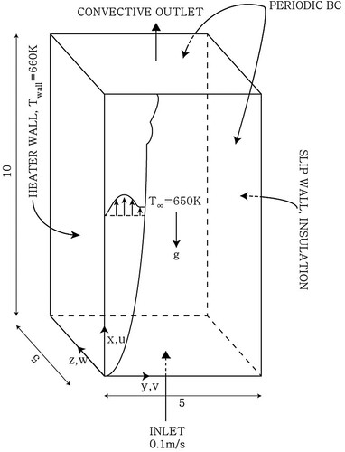
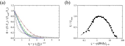
Figure (a) shows profiles of the average temperature along the wall normal direction. Temperature is normalized by the temperature difference between and
. If the Rayleigh number is less than
, natural convection is considered to be laminar. Profiles of the predicted normalized temperature are found to agree well with the similarity solutions in the laminar flow regime. Since similarity solutions do not exist in the turbulent flow regime, temperature profiles which are numerically predicted are only presented. The profile of the time-averaged velocity is also compared with the experimental data as shown in Figure (b). The streamwise velocity is normalized by the free stream velocity along the dimensionless transverse coordinate defined as
. The Grashof number in the present study is
, and the simulation result is in good agreement with the experimental data at
. In those Grashof number regimes, the buoyancy force dominates the viscous force causing natural convection.
Figure 2. (a) Profiles of the time-averaged temperature along the wall normal direction. Present simulation ▵, ; °,
; □,
; – –,
;
,
. Similarity solution –,
; –,
; –,
. (b) Profile of the time-averaged velocity along the wall normal direction. –, present study (
); ▴, Cheesewright (Citation1968) (
); •, Smith (Citation1972) (
); ▪, Miyamoto et al. (Citation1982) (
).
3.2. Validation of the chemical reaction model
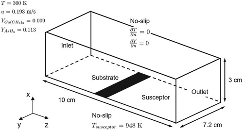
The chemical reaction model is validated for predicting the growth rate of a GaAs film. Ern et al. (Citation1996) conducted the numerical study on a CVD process to deposit a GaAs film by injecting trimethylgallium (Ga(CH)
) and arsine (AsH
) gases in a horizontal channel reactor. Ern et al. considered detailed chemical reactions in gases and on substrate surfaces, which were also studied by Mountziaris and Jensen (Citation1991).
A schematic illustration of the computational domain and boundary conditions for the horizontal channel reactor is depicted in Figure . A susceptor is attached to the right behind the substrate located on the reactor bottom. An operating gas flows into the domain at a constant velocity of 0.193 m/s with no-slip conditions on the side walls. The wall-normal gradients of temperature and species-concentration are zero on the wall boundaries. A constant temperature condition of 948 K is applied to the substrate and the susceptor. Ga(CH)
and AsH
are diluted in the carrier gas H
and fed into the reactor. The partial pressure of Ga(CH
)
is
and the partial pressure of AsH
is
. The total pressure is 1 atm. Under these conditions, the Reynolds number Re is 190 based on the reactor length in the streamwise direction. The computational domain is filled with a full hexahedral mesh where a total of 430,920 grid cells (
) is used. At least 4 cells are placed within the turbulent wall-unit of unity near the walls. The gas-phase and surface chemical reactions considered are described in detail by Ern et al. (Citation1996) and Mountziaris and Jensen (Citation1991).
Figure 3. Schematic diagram of the computational domain and boundary conditions for the simulation of the horizontal channel reactor. The substrate and the susceptor temperature is maintained at 948 K.
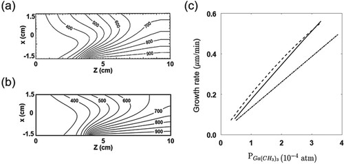
The results of the present study are compared to the experimental (Reep & Ghandhi, Citation1983) and numerical ones (Ern et al., Citation1996). Figure shows the temperature isolines at the middle plane (). The growth rates of the GaAs thin-film for varying Ga(CH
)
partial pressures are also depicted in the figure. Specifically, Figure (a) shows the numerical result of Ern et al. (Citation1996) for the temperature distribution in the reactor and (b) shows the result of the present study. High temperature gradients are shown along the substrate and the susceptor with the outlet temperature of 700–984 K. Figure (c) shows the growth rates of the GaAs thin-film on the substrate as a function of the partial pressure of Ga(CH
)
. The GaAs growth rates are linearly proportional to the Ga(CH
)
pressure and therefore the film growth is significantly affected by the transport of the Ga(CH
)
gas. The present results are consistent with those of Ern et al.. However, at a low Ga(CH
)
pressure, the growth rate predicted by the present work is found to be slightly closer to the experimental result (Reep & Ghandhi, Citation1983). In general, the growth rates in the numerical studies are predicted to be higher than experimental results because the numerical methods assume that the surface reaction occurs in a single control volume, which is right on the surface. Therefore, the chemical reaction can be somewhat overly predicted.
Figure 4. Contours of isotherms in the reactor with the susceptor temperature of 948 K; partial pressure of Ga(CH)
:
; partial pressure of AsH
:
; and total pressure: 1.0 atm. (a) The numerical result of Ern et al. (Citation1996) and (b) the present result. (c) The growth rate of the GaAs layer as a function of Ga(CH
)
partial pressure. – · –, experimental result of Reep and Ghandhi (Citation1983); – –, numerical result of Ern et al. (Citation1996); and —, the present result.
3.3. Validation of the efficiency-prediction model
The National Renewable Energy Laboratory (NREL) (Contreras et al., Citation1999) reported a CIGS solar cell with an efficiency of 18.8% fabricated by a three-stage co-evaporation process. The deposited CIGS layer had a thickness of and a band-gap energy of 1.2 eV. Song et al. (Citation2004) made an attempt to numerically predict the electrical performance of the NREL's solar cell. They solved a Poisson equation for electrostatic potential and continuity equations for free holes and electrons using the AMPS–1D simulation tool. Similarly, the efficiency-prediction model, in the present work, is validated by estimating the performance of the NREL's solar cell in comparison to Song et al.. The simulation parameters used are the measured thickness (
) and Ga ratio (
) from the NREL (Contreras et al., Citation1999). The charge-carrier concentration (
) and the ideal factor (m = 1.5) are selected as optimal values to fitting the measured performance curves.
The predicted results of the present model are found to well agree with the experimental and the numerical results as shown in Table . The values of predicted by the numerical simulations show a slight difference of
compared to the experimental result.
is predicted as low as 0.8 mA/cm
by Song et al. and as low as 0.58 mA/cm
by the present model. The fill factor is predicted to be 0.75% higher in Song et al. while 0.23% higher in the present simulation. The conversion efficiency of the CIGS solar cell is predicted to be slightly lower than that in the experiment. The current density–voltage (J–V) curve and the IQE are presented in Figure . The present model well predicts the J–V curve as shown in Figure (a). Figure (b) shows the IQE as a function of wavelengths from 600 nm to 1200 nm with good agreements. Overall, the present model is found to well predict the performance of the CIGS solar cells.
Figure 5. (a) Current density and voltage (J–V) curve and (b) internal quantum efficiency curve as a function of the wavelength. •, Experimental results of Contreras et al. (Citation1999); – –, numerical results of Song et al. (Citation2004); and —, the present results.
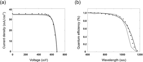
Table 2. Comparison of a solar cell performance with the experiment (Contreras et al., Citation1999) and numerical study (Song et al., Citation2004) regarding the open-circuit voltage , short-circuit current density
, fill factor FF, and efficiency η.
4. Simulation of the selenization process
The selenization process is a chemical vapor deposition process. Cu, Ga, and In are sputtered on substrates and exposed to HSe gas. The H
Se gas is directly absorbed by the sputtered substrates or decomposed into Se elements. As the absorbed or decomposed Se reacts with the sputtered atoms, Cu, Ga, and In produce CuSe
, CuSe, Cu
Se, GaSe, Ga
Se
, In
Se
, and InSe binaries. Those binary compounds become ternary compounds which are CuInSe
and CuGaSe
at around 730 K. Finally, the CIGS compound, Cu(In, Ga)Se
, is formed at around 800 K. Those surface reactions are very sensitive to the substrate temperature. In following sections, the velocity and temperature fields during the heat-up and stabilization steps are analyzed. Chemical reactions in the selenization process including dissociation of H
Se gas and growth of the CIGS layer are also considered. Based on the predicted layer thickness and the Ga ratio, the conversion efficiency is evaluated using an efficiency-prediction model.
4.1. Computational configurations
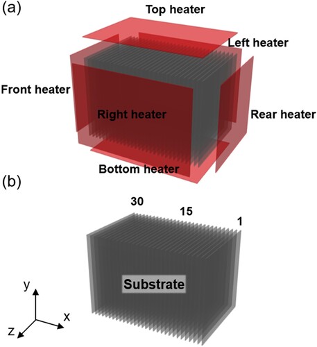
A comprehensive simulation of a selenization process for batched substrates of several square meters is provided in this section. The structure of an industrial CVD reactor considered is depicted in Figure . Due to some confidential issues, the exact shape of the reactor and the detailed selenization recipes can not be presented here. Briefly, as shown in Figure (a,b), heaters surround side-, top-, and bottom-walls, and two boats are located on the front side and the rear side in the reactor. 30 substrates are vertically batched with narrow intervals in the boats. Physical quantities are normalized by their reference values selected.
Figure 6. Schematic diagram of the thermal reactor. (a) The reactor is surrounded by heaters and (b) 30 substrates are placed in the reactor.
As the heater temperature increases, natural convection develops along vertical walls. The turbulent convection transports energy and chemical species to the substrates. Since the reactor is sealed during the process, all boundaries are treated with no-slip conditions for the momentum equations. On the heater surfaces, temperature profiles from the experiment (Yu et al., Citation2018) are directly imposed with Dirichlet conditions. Adiabatic conditions are imposed outside of the reactor. For chemical species, the mass fraction is assumed to be zero at the wall and the heater, whereas normal gradients of the mass fraction become zero on the substrate surface.
The HSe gas diluted by N
is injected into the thermal reactor and the total pressure becomes 0.92 atm. The partial pressure of H
Se gas is 0.02 atm, and the partial pressure of N
is 0.90 atm. It is noted that a mixture of the working gases used in the selenization process does not participate in thermal radiation since the nitrogen gas, which makes up the majority of the total pressure, is transparent to infrared radiation.
The normalized process time τ is defined as a ratio of elapsed time to the entire process time. The normalized heater temperature θ is defined as follows:
(31)
(31) where
is the minimum heater temperature and
is the maximum heater temperature. The selenization process is divided into two sub-steps. The first sub-step is referred to as a heat-up step, and the second step is a stabilization step. The heaters increase the temperature inside during the heat-up step and then are adjusted to maintain a constant temperature during the stabilization step. The material properties of the working gases are given as a function of temperature.
A solid domain is constructed with a full hexahedral mesh of 0.1 million grid cells. A grid for the fluid domain consists of a total of 7 million hexahedral cells. Since the turbulent convection occurs due to the high temperature-gradients near the heaters, at least 4 cells are allocated within the distance of 1 wall unit from the fluid boundaries. No meaningful differences in the simulations results were found by further refinement of grid resolution for fluid and solid domains to 12.7 million cells and 0.28 million cells, respectively.
4.2. Thermal-fluid flow during the selenization
Accurate prediction of fluid motions and heat transfer during the selenization is important because the concentration and reaction of chemical species are significantly influenced by the thermal-fluid flow inside. The time-averaged velocities and temperature fields at several locations are investigated at two normalized time points, and
. Specifically,
is in the heat-up step with a ramping rate of 0.09 K/s, and
is in the stabilization step where the heater temperature is kept constant. Based on the average temperature and the mean velocity magnitude, the heat-up step is in the turbulence regime of
and
.
Contours of the y-directional velocity and temperature are given in Figure on an xy-plane slicing the middle of the reactor. The velocity and temperature are averaged for 5 minutes which corresponds to at
. Figure (a) shows the magnitude of y-velocity. To develop circulating flow inside, vertical heaters on the side walls have higher temperature profiles than the bottom heater. In particular, due to the high temperature on the rear-side heater, strong upward flow forms near the rear wall. When the rising flow reaches the top, it starts to descend toward the bottom of the reactor. The descending flow passes through narrow passages between the substrates as shown in Figure (a). However, the descending flow is not uniform across the substrates. Furthermore, some reverse flow coming out from the passages is often observed at the top of the substrates. The time-averaged temperature distribution at
is presented in Figure (c). As expected, the raised hot gas is extensively distributed at the top area of the reactor. The hot gas heats the top region of the substrates first and gradually raises the temperature of the entire region.
Figure 7. Contours of the y-directional velocity time-averaged for in the mid-section x−y plane of the reactor at (a)
and (b)
. Contours of the temperature time-averaged for
in the mid-section x−y plane of the reactor at (c)
and (d)
.
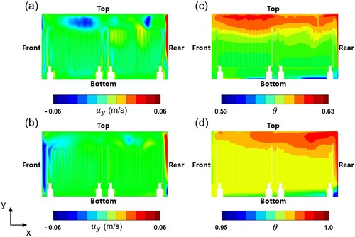
At the stabilization step, , similar flow patterns and similar temperature distributions appear. Figure (b) presents the magnitude of the y-velocity. Strong upward flow still exists near the rear heater whereas strong downdraft newly appears at the front wall. The downdraft blows the stagnant hot gas down as shown in Figure (d). In the stabilization step, relatively uniform distributions of the flow velocity and temperature are observed in the passages between the substrates compared to the heat-up step.
The surface temperature of the substrate is an important factor that determines the rates of surface chemical reactions. Figure shows time-averaged temperature contours on 15th and 23rd substrates at . The present results are averaged for 5 minutes (
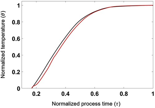
) and the experimental data from 9 temperature-sensors are also averaged for the same time interval. The temperature is normalized by the difference between the maximum and the minimum temperatures on the substrate. Considering that the temperature fields were averaged for only 5 minutes which are far from the averaging duration for full statistical convergence for both experimental and numerical results, the comparison is rather qualitative than quantitative. It is found that both measured and predicted temperature fields have radial patterns such that a low temperature zone appears in the center of the substrates. Symmetric temperature fields are observed in the simulation result while the temperature distributions are found to be anti-symmetric in the experiment as shown in Figure . Since the amount of heat energy generated by the left and right heaters is the same, it is considered that anti-symmetry of outgoing heat flux from the external surface of the reactor, which is difficult to precisely control in the experiment, caused anti-symmetric distributions of temperature on substrate surfaces in the experiment. Figure shows the spatially averaged temperature for all substrates batched during the selenization process. The black line indicates the experimental result, whereas the red line indicates the predicted result.
Figure 8. Temperature distributions on the 15th and 23rd substrates at . Temperature is averaged for 5 minutes (
). The experimental results: (a) the 15th and (b) the 23rd substrates. Results of the present study: (c) the 15th and (d) the 23rd substrates.
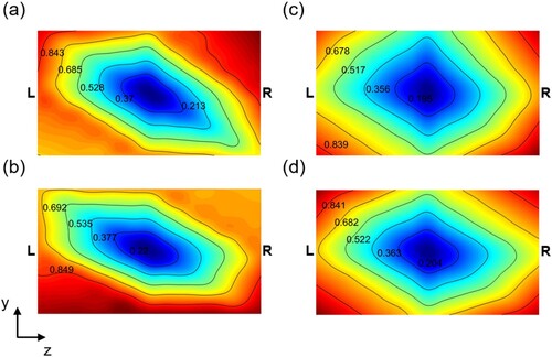
Figure 9. Spatially averaged temperature profile during the selenization process. The black line indicates temperature measured by the experiment, while the red line indicates the temperature predicted by the present study.
4.3. Chemical reactions during the selenization
When temperature increases, HSe is decomposed into H
and Se
. The H
Se gas and the decomposed Se element participate in surface adsorption and react with the deposited precursor to form binary compounds. Therefore, their concentration is important for prediction of the chemical composition of the grown CIGS layer. The present study considers both forward and reverse reactions of the thermal decomposition. The gas concentration (H
Se and Se
), y-velocity, and temperature are analyzed on an yz-plane in the middle of a passage between two substrates. Figure shows time-averaged contours on the yz-plane in the middle of the passage between the 1st and 2nd substrates for
. In Figure (a), strong ascending flow is developed along the left and right walls and then the flow goes down right after reaching the top wall. The temperature distribution is presented in Figure (c), and the mole fraction of H
Se is shown in Figure (b). As H
Se is rapidly decomposed into H
and Se
at a high temperature environment, the mole fraction of H
Se has the opposite distribution against the temperature field, i.e. a high-temperature region has a low mole fraction of H
Se. In the same context, the mole fraction of Se
has the distribution opposite to the mole-fraction field of H
Se as shown in Figure (d). Since the decomposition rate is an exponential function for temperature, the concentrations of H
Se and Se
are inhomogeneous across the substrate's surface resulting in the non-uniform surface-reaction rates.
Figure 10. Contours time-averaged for 5 minutes () near the 1st substrate at
: (a) the y-directional velocity, (b) the mole fraction of H
Se, (c) normalized temperature, and (d) the mole fraction of Se
.
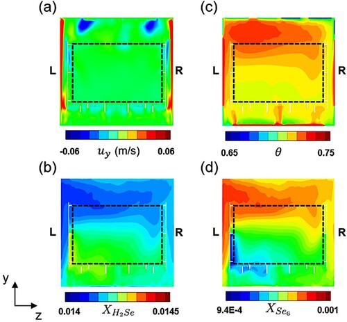
Figure shows the predicted thickness and Ga ratio in the CIGS layer at the 1st and 16th substrates. The thickness and the Ga ratio are important parameters for evaluating band-gap energy and conversion efficiency of the CIGS solar cell. In the 1st substrate, the layer of CIGS compounds, approximately thick, is deposited as illustrated in Figure (a). The layer thickness is about
on the bottom region but about
on the top region, specifically. The thickness isolines present a wavy pattern on the top region. On the 16th substrate, the CIGS layer grows much thicker as shown in Figure (b). Due to the hot gas blowing from the top and bottom areas of the reactor, the CIGS layer grows much thicker than other substrates, however, the non-uniformity in thickness becomes more severer.
Figure 11. Predicted CIGS layer thicknesses on (a) the 1st substrate and (b) 16th substrate. Predicted Ga ratios on (c) the 1st substrate and (d) the 16th substrate.
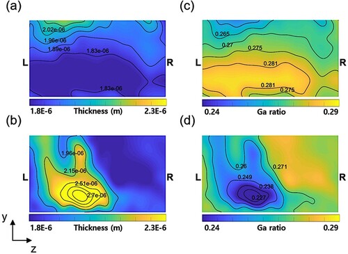
Across the whole substrates, the Ga ratio ranges from 0.23 to 0.29, which is close to the optimum value of 0.3. Figure (c) shows the predicted Ga ratio on the 1st substrate. The ratio on the top region in the substrate is about 0.26, whereas the bottom region is as high as 0.28. It means that the CIGS layer grows more on the top region with a lower Ga content, whereas grows less at the bottom region with a higher Ga content. As shown in Figure (c), the contour presents a wavy pattern on the top and bottom edges where the Ga content is low. This pattern is more pronounced on the 16th substrate as shown in Figure (d). The Ga content on the left side of the substrate is about 0.23, showing a marked difference from that on the right side which is about 0.27. It means that CuInSe grows more on the left side, but less on the right side of the substrate and vice versa for CuGaSe
.
4.4. Conversion efficiency of the solar cell
Using the predicted CIGS thickness and Ga ratio, cell-efficiency can be evaluated from the efficiency-prediction model. The Ga ratio is used to calculate band-gap energy using Equation (Equation22(22)
(22) ). The current density is then obtained by Equation (Equation30
(30)
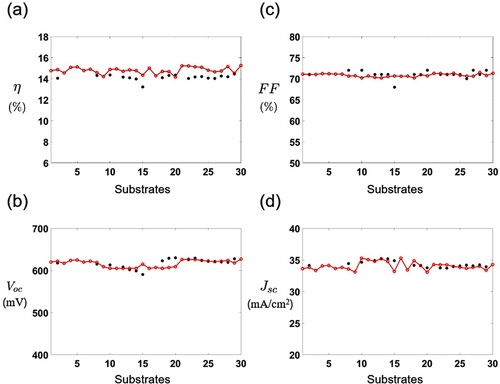
(30) ) using the predicted thickness and band-gap energy in the consideration of shunt resistance and series resistance measured in the experiment. Figure shows several performance parameters for each substrate. Figure (a) shows the conversion efficiency of each substrate under the standard test conditions. The efficiency is predicted to be on average 0.67% higher than the experimental data. The fill factor is measured to evaluate cell performance as a function of the open-circuit voltage and the short-circuit current density. Figure (b) presents the open-circuit voltage (
). The 15th substrate has a slightly higher value in
than the experimental results, whereas the 18th, 19th, and 20th substrates present lower values than the experimental data. The overall
is predicted to be 1.53 mV lower. The fill factor is given in Figure (c). The predicted fill factor has a more uniform distribution than the experimental results. The averaged fill factor is calculated to be 0.23% lower than the experimental values. Meanwhile, the short-circuit current density (
) is predicted to be lower than the experimental ones on the 15th and 20th substrates as shown in Figure (d). The
is predicted to be on average 0.22 mA/cm
lower. Overall, the performance parameters of each substrate are accurately predicted.
Figure 12. CIGS solar cell performance along the substrates: (a) the conversion efficiency η, (b) open-circuit voltage , (c) fill factor FF, and (d) short-circuit current density
. •, experimental results and red• with a red line, the present results.
In the present work, there are two limitations that explain small deviation in the predicted parameters. First, the prediction model does not account for physics in a molecular scale such as grain boundaries, defects, and doping. The second limitation is that the present work ignores the diffusion of molecules within the CIGS layer by applying the concept of site fraction. By considering the molecular-scale physics and the diffusion of the molecules, it is expected that the prediction accuracy of the model can be further improved (Idris et al., Citation2015; W. Li et al., Citation2019).
4.5. Stain formation affecting the cell performance
Factors that affect the stain formation during the selenization are analyzed in this section. Figure (a) shows the conversion efficiency on the 16th substrate measured from the experiment. Figure (b) presents the electroluminescent image of this substrate. The dark stains in the image, where the efficiency is low, extensively appear on the left side of the substrate. The bright stains, where the efficiency is high, appear on the right side of the substrate. Figure (c) and (d) show the predicted temperature and Ga ratio of the substrate, respectively. The temperature on the left side of the substrate is predicted to be significantly higher than that on the right side. Similarly, Figure (d) shows the non-uniform distribution of the predicted Ga ratio. The Ga ratio is low on the left side but high on the right side. These distribution patterns are well matched with the efficiency map and the electroluminescent image as shown in Figure (a,b) from the experiment. The present work has found that, in the dark stains, the Ga ratio is low due to the high temperature indicating that CuInSe grows excessively compared to CuGaSe
resulting in low conversion efficiency. It means that the dark stains will become more pronounced when an uneven distribution of hot gas-flow occurs through the passages between substrates reducing the cell-performance.
Figure 13. Experimental results on the 16nd substrate: (a) contour of the measured conversion efficiency and (b) the electroluminescence image. Numerical results: (c) contour of the temperature time-averaged for 5 minutes () at
and (d) contour of the predicted Ga ratio.
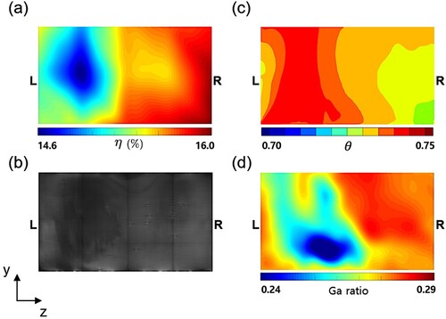
Figure 14. Experimental results on 19th substrate: (a) contour of the measured conversion efficiency and (b) the electroluminescence image. Numerical results: (c) contour of the instantaneous y-directional velocity at and (d) contour of the predicted Ga ratio.

In the present reactor, wavy stains appear on the top and bottom regions of the substrates. Figure (a,b) show the measured efficiency map and electroluminescence image of the 19th substrate, respectively. Notably, a distinct wavy pattern appears in the dark stains at the top region of the substrate. Ascending and descending gas flow near the top region is believed to be the cause of the wavy pattern. Figure (c) shows the predicted instantaneous-velocity distribution of the gas flow rising and falling near the top region. Similarly, the Ga ratio is predicted to be low on the top region, exhibiting a wavy pattern, and to be high at the bottom region as shown in Figure (d).
In summary, from the present analysis, it is found that the behaviors of the gas flow determine the shape of the stains occurring at the top or bottom of the substrates, while the brightness of the stains, i.e. efficiency, is strongly influenced by the temperature distribution on the substrate. From the binary phase diagram of CuInSe reported in experimental studies (Muzzillo et al., Citation2016; Regmi et al., Citation2020), the concentration of Se
gas generated by thermal decomposition determines the ratio of binaries that determines the conversion efficiency of solar cells, which supports the present analysis.
5. Concluding remarks
A comprehensive analysis of the selenization on large-area substrates has been performed with the consideration of thermal-fluid flow and detailed chemical reactions in an industrial CVD reactor. The performance parameters, i.e. efficiency, fill-factor, open-circuit voltage, and short-circuit current, are evaluated from the solution of a diffusion equation for charge-carriers in the CIGS thin-layer.
Non-uniform thermal-fluid flow is identified through the vertical velocity fields and the temperature distributions on the substrates. The problem is that the descending flow is not uniformly rectified before entering the passages between substrates. Therefore, the supply of heat energy and gas-species becomes uneven across the substrates. From the instantaneous velocity field, in particular, a strong disturbance is identified near the top regions of the substrates where the descending flow first arrives. In terms of the chemical reactions, the uneven temperature distribution causes spatially non-uniform decomposition of HSe gas inside the reactor resulting the uneven growth of the CIGS layer.
In addition, the stain formation on large-area substrates is investigated. The uneven temperature distribution on the substrate is identified as a major cause of the stain formation. Furthermore, the shape of the stain appears to be affected by the velocity pattern of the gas flow. This result suggests that the stain formation due to the uneven distribution of temperature can be alleviated by rectifying the thermal-fluid flow such that the flow rates become uniform before entering the passages between the substrates. Attaching appropriate baffles on the top of the substrates may be a feasible way of achieving this (Fauzi et al., Citation2018).
As a future direction of the present research, it is considered to incorporate models for molecular-scale dynamics (Idris et al., Citation2015; W. Li et al., Citation2019) which can explain the characteristics of micro-structures on the substrate.
Disclosure statement
No potential conflict of interest was reported by the author(s).
Additional information
Funding
References
- Aghaei, A., Bhattacharyya, S., Dezfulizadeh, A., Goldanlou, A. S., Rostami, S., & Sharifpur, M. (2021). Heat transfer and fluid flow analysis using nanofluids in diamond-shaped cavities with novel obstacles. Engineering Applications of Computational Fluid Mechanics, 15(1), 1034–1056. https://doi.org/10.1080/19942060.2021.1930170
- Alonso, J., Hahn, S., Ham, F., Herrmann, M., Iaccarino, G., Kalitzin, G., LeGresley, P., Mattsson, K., Medic, G., Moin, P., Pitsch, H., Schluter, J., Svard, M., van der Weide, E., You, D., & Wu, X. (2006). CHIMPS: A high-performance scalable module for multi-physics simulations. In 42nd AIAA/ASME/SAE/ASEE Joint Propulsion Conference & Exhibit, 5274.
- Atkins, P., & De Paula, J. (2009). Elements of physical chemistry. Macmillan.
- Beck, M. E., Swartzlander-Guest, A., Matson, R., Keane, J., & Noufi, R. (2000). CuIn(Ga)Se 2-based devices via a novel absorber formation process. Solar Energy Materials and Solar Cells, 64(2), 135–165. https://doi.org/10.1016/S0927-0248(00)00066-0
- Cheesewright, R. (1968). Turbulent natural convection from a vertical plane surface. Journal of Heat Transfer, 90(1), 1–6. https://doi.org/10.1115/1.3597453
- Chen, S. C., Wang, S. W., Kuo, S. Y., Juang, J. Y., Lee, P. T., Luo, C. W., K. H. Wu, & Kuo, H. C. (2017). A comprehensive study of one-step selenization process for Cu(In 1−x Ga x)Se 2 thin film solar cells. Nanoscale Research Letters, 12(1), 208. https://doi.org/10.1186/s11671-017-1993-0
- Choi, K., & Kim, J. W. (2014). CFD simulation of chemical vapor deposition of silicon carbide in CH 3SiCl 3-H 2 system. Current Nanoscience, 10(1), 135–137. https://doi.org/10.2174/1573413709666131109003414
- Contreras, M. A., Egaas, B., Ramanathan, K., Hiltner, J., Swartzlander, A., Hasoon, F., & Noufi, R. (1999). Progress toward 20 % efficiency in Cu(In, Ga)Se 2 polycrystalline thin-film solar cells. Progress in Photovoltaics: Research and Applications, 7(4), 311–316. https://doi.org/10.1002/(ISSN)1099-159X
- Decock, K., Lauwaert, J., & Burgelman, M. (2010). Characterization of graded CIGS solar cells. Energy Procedia, 2(1), 49–54. https://doi.org/10.1016/j.egypro.2010.07.009
- Delgado-Sanchez, J. M., López-González, J. M., Orpella, A., Sánchez-Cortezon, E., Alba, M. D., López-López, C., & Alcubilla, R. (2017). Front contact optimization of industrial scale CIGS solar cells for low solar concentration using 2D physical modeling. Renewable Energy, 101, 90–95. https://doi.org/10.1016/j.renene.2016.08.046
- Dhondt, G. (2004). The finite element method for three-dimensional thermomechanical applications. John Wiley & Sons.
- Dullweber, T., Rau, U., Contreras, M. A., Noufi, R., & Schock, H.-W. (2000). Photogeneration and carrier recombination in graded gap Cu(In, Ga)Se 2 solar cells. IEEE Transactions on Electron Devices, 47(12), 2249–2254. https://doi.org/10.1109/16.887004
- Ern, A., Giovangigli, V., & Smooke, M. D. (1996). Numerical study of a three-dimensional chemical vapor deposition reactor with detailed chemistry. Journal of Computational Physics, 126(1), 21–39. https://doi.org/10.1006/jcph.1996.0117
- Fauzi, F., Ismail, E., Ani, M., Syed Abu Bakar, S., Mohamed, M., Majlis, B., & Azam Mohd Abid, M. (2018). A critical review of the effects of fluid dynamics on graphene growth in atmospheric pressure chemical vapor deposition. Journal of Materials Research, 33(9), 1088–1108. https://doi.org/10.1557/jmr.2018.39
- Frantz, J. A., Myers, J. D., Bekele, R. Y., Nguyen, V. Q., Sadowski, B. M., S. I. Maximenko, Walters, R. J., & Sanghera, J. S. (2015). Recent progress in sputtered Cu(In, Ga)Se 2 absorbers for photovoltaics. In Advanced Photonics 2015 (OSA Technical Digest, NS3B.2).
- Ghalandari, M., Bornassi, S., Shamshirband, S., Mosavi, A., & Chau, K. W. (2019). Investigation of submerged structures' flexibility on sloshing frequency using a boundary element method and finite element analysis. Engineering Applications of Computational Fluid Mechanics, 13(1), 519–528. https://doi.org/10.1080/19942060.2019.1619197
- Ghorbani, T., Zahedifar, M., Moradi, M., & Ghanbari, E. (2020). Influence of affinity, band gap and ambient temperature on the efficiency of CIGS solar cells. Optik, 223, 165541. https://doi.org/10.1016/j.ijleo.2020.165541
- Gloeckler, M., Fahrenbruch, A., & Sites, J. (2003). Numerical modeling of CIGS and CdTe solar cells: Setting the baseline. Proceedings of the 3rd World Conference on Photovoltaic Energy Conversion, IEEE.
- Gulkowski, S., & Krawczak, E. (2020). RF/DC magnetron sputtering deposition of thin layers for solar cell fabrication. Coatings, 10(8), 791. https://doi.org/10.3390/coatings10080791
- Hanna, G., Jasenek, A., Rau, U., & Schock, H. (2001). Influence of the Ga-content on the bulk defect densities of Cu(In, Ga)Se 2. Thin Solid Films, 387(1–2), 71–73. https://doi.org/10.1016/S0040-6090(00)01710-7
- Houck, D. W., Siegler, T. D., & Korgel, B. A. (2019). Predictive modeling of CuInSe 2 nanocrystal photovoltaics: The importance of band alignment and carrier diffusion. ACS Applied Energy Materials, 2(2), 1494–1504. https://doi.org/10.1021/acsaem.8b02090
- Idris, B., Rafik, Z., Kamal, D., Abdessalam, B., & Faouzi, G. (2015). Size and grain-boundary effects on the performance of polycrystalline CIGS-based solar cells. In IREC2015 the Sixth International Renewable Energy Congress, IEEE.
- Karar, O., Emani, S., Marappa Gounder, R., Myo Thant, M. M., Mukhtar, H., Sharifpur, M., & Sadeghzadeh, M. (2021). Experimental and numerical investigation on convective heat transfer in actively heated bundle-pipe. Engineering Applications of Computational Fluid Mechanics, 15(1), 848–864. https://doi.org/10.1080/19942060.2021.1920466
- Kaur, I., Pandya, D. K., & Chopra, K. L. (1980). Growth kinetics and polymorphism of chemically deposited CdS films. Journal of the Electrochemical Society, 127(4), 943–948. https://doi.org/10.1149/1.2129792
- Kim, S., Kim, W. K., Kaczynski, R., Acher, R., Yoon, S., Anderson, T., Crisalle, O., Payzant, E., & Li, S. (2005). Reaction kinetics of CuInSe 2 thin films grown from bilayer InSe/CuSe precursors. Journal of Vacuum Science & Technology A: Vacuum, Surfaces, and Films, 23(2), 310–315. https://doi.org/10.1116/1.1861051
- Kim, W. K., Kim, S., Payzant, E. A., Speakman, S., Yoon, S., Kaczynski, R., Acher, R., Anderson, T., Crisalle, O., Li, S., & Craciun, V. (2005). Reaction kinetics of α-CuInSe 2 formation from an In 2Se 3/CuSe bilayer precursor film. Journal of Physics and Chemistry of Solids, 66(11), 1915–1919. https://doi.org/10.1016/j.jpcs.2005.09.074
- Kim, W. K., Payzant, E. A., Anderson, T. J., & Crisalle, O. (2007). In situ investigation of the selenization kinetics of Cu–Ga precursors using time-resolved high-temperature X-ray diffraction. Thin Solid Films, 515(15), 5837–5842. https://doi.org/10.1016/j.tsf.2006.12.173
- Kim, W. K., Payzant, E. A., Kim, S., Speakman, S. A., Crisalle, O., & Anderson, T. (2008). Reaction kinetics of CuGaSe 2 formation from a GaSe/CuSe bilayer precursor film. Journal of Crystal Growth, 310(12), 2987–2994. https://doi.org/10.1016/j.jcrysgro.2008.01.034
- Kim, W. K., Payzant, E. A., Yoon, S., & Anderson, T. J. (2006). In situ investigation on selenization kinetics of Cu–In precursor using time-resolved, high temperature X-ray diffraction. Journal of Crystal Growth, 294(2), 231–235. https://doi.org/10.1016/j.jcrysgro.2006.05.066
- Li, C., Yang, Y., Spataru, S., Zhang, K., & Wei, H. (2021). A robust parametrization method of photovoltaic modules for enhancing one-diode model accuracy under varying operating conditions. Renewable Energy, 168, 764–778. https://doi.org/10.1016/j.renene.2020.12.097
- Li, W., Yan, X., Aberle, A. G., & Venkataraj, S. (2019). Effect of sodium diffusion on the properties of CIGS solar absorbers prepared using elemental Se in a two-step process. Scientific Reports, 9(1), 2637. https://doi.org/10.1038/s41598-019-39283-2
- Liu, Y. H., Peng, G. J., Lai, W. C., Huang, C. Y., & Liang, J. H. (2017). Flow field investigation in a rotating disk chemical vapor deposition chamber with a perforated showerhead. Experimental Thermal and Fluid Science, 88, 389–399. https://doi.org/10.1016/j.expthermflusci.2017.06.018
- Luo, S., Wang, P., Zhang, H., Zhang, S., & Zheng, L. (2021). Numerical study on chemical vapor deposition of ZrC and optimization of deposition uniformity with flexible flow controller. Materials Today Communications, 27, 102318. https://doi.org/10.1016/j.mtcomm.2021.102318
- Minoura, S., Kodera, K., Maekawa, T., Miyazaki, K., Niki, S., & Fujiwara, H. (2013). Dielectric function of Cu(In, Ga)Se 2-based polycrystalline materials. Journal of Applied Physics, 113(6), 063505. https://doi.org/10.1063/1.4790174
- Miyamoto, M., Kajino, H., Kurima, J., & Takanami, I. (1982). Development of turbulence characteristics in a vertical free convection boundary layer. Heat Transfer, 2, 323–328. https://doi.org/10.1615/IHTC7.3320
- Mohammadnejad, S., & Parashkouh, A. B. (2017). CZTSSe solar cell efficiency improvement using a new band-gap grading model in absorber layer. Applied Physics A, 123(12), 1–9. https://doi.org/10.1007/s00339-017-1371-x
- Mountziaris, T. J., & Jensen, K. F. (1991). Gas-phase and surface reaction mechanisms in MOCVD of GaAs with trimethyl-gallium and arsine. Journal of the Electrochemical Society, 138(8), 2426. https://doi.org/10.1149/1.2085990
- Muzzillo, C. P., Campbell, C. E., & Anderson, T. J. (2016). Cu-Ga-In thermodynamics: Experimental study, modeling, and implications for photovoltaics. Journal of Materials Science, 51(7), 3362–3379. https://doi.org/10.1007/s10853-015-9651-3
- Nakamura, M., Yamaguchi, K., Kimoto, Y., Yasaki, Y., Kato, T., & Sugimoto, H. (2019). Cd-free Cu(In, Ga)(Se, S) 2 thin-film solar cell with record efficiency of 23.35%. IEEE Journal of Photovoltaics, 9(6), 1863–1867. https://doi.org/10.1109/JPHOTOV.5503869
- Noh, Y., Kim, Y., Park, S., Kim, B. K., & Kim, H. J. (2019). Applications of vertical cavity surface emitting lasers for low-pressure chemical vapor deposition reactors. International Journal of Heat and Mass Transfer, 141, 245–255. https://doi.org/10.1016/j.ijheatmasstransfer.2019.06.078
- Purwins, M., Weber, A., Berwian, P., Müller, G., Hergert, F., Jost, S., & Hock, R. (2006). Kinetics of the reactive crystallization of CuInSe 2 and CuGaSe 2 chalcopyrite films for solar cell applications. Journal of Crystal Growth, 287(2), 408–413. https://doi.org/10.1016/j.jcrysgro.2005.11.054
- Rau, U., & Schock, H.-W. (1999). Electronic properties of Cu(In, Ga)Se 2 heterojunction solar cells–recent achievements, current understanding, and future challenges. Applied Physics A: Materials Science & Processing, 69(2), 131–147. https://doi.org/10.1007/s003390050984
- Reep, D., & Ghandhi, S. (1983). Deposition of GaAs epitaxial layers by organometallic CVD: Temperature and orientation dependence. Journal of the Electrochemical Society, 130(3), 675. https://doi.org/10.1149/1.2119780
- Regmi, G., Ashok, A., Chawla, P., Semalti, P., Velumani, S., Sharma, S. N, & Castaneda, H. (2020). Perspectives of chalcopyrite-based CIGSe thin-film solar cell: A review. Journal of Materials Science: Materials in Electronics, 31(10), 7286–7314. https://doi.org/10.1007/s10854-020-03338-2
- Reinhold-López, K., Braeuer, A., Schmitt, A., Popovska-Leipertz, N., & Leipertz, A. (2012). Flow field characterization in a vertically oriented cold wall CCVD reactor by particle image velocimetry. Chemical Engineering Journal, 184, 315–325. https://doi.org/10.1016/j.cej.2012.01.062
- Salih, S. Q., Aldlemy, M. S., Rasani, M. R., Ariffin, A. K., Ya, T. M. Y. S. T., Al-Ansari, N., Yaseen, Z. M., & Chau, K. W. (2019). Thin and sharp edges bodies-fluid interaction simulation using cut-cell immersed boundary method. Engineering Applications of Computational Fluid Mechanics, 13(1), 860–877. https://doi.org/10.1080/19942060.2019.1652209
- Smith, R. R. (1972). Characteristics of turbulence in free convection flow past a vertical plate [Ph.D. thesis, Queen Mary University of London].
- Soedergren, S., Hagfeldt, A., Olsson, J., & Lindquist, S.-E. (1994). Theoretical models for the action spectrum and the current-voltage characteristics of microporous semiconductor films in photoelectrochemical cells. Journal of Physical Chemistry, 98(21), 5552–5556. https://doi.org/10.1021/j100072a023
- Song, J., Li, S. S., Huang, C., Crisalle, O., & Anderson, T. (2004). Device modeling and simulation of the performance of Cu(In 1−x, Ga x)Se 2 solar cells. Solid-State Electronics, 48(1), 73–79. https://doi.org/10.1016/S0038-1101(03)00289-2
- Stölzel, M., Algasinger, M., Zelenina, A., Weber, A., Sode, M., Schubbert, C., Eraerds, P., Lechner, R., Dalibor, T., & Palm, J. (2019). Absorber optimization in CIGSSe modules with a sputtered ZnOS buffer layer at 19% efficiency. In 36th European Photovoltaic Solar Energy Conference and Exhibition, EU PVSEC.
- Vahedein, Y. S., & Schrlau, M. G. (2016). Numerical investigation of thermofluid flow in a chemical vapor deposition furnace utilized to manufacture template-synthesized carbon nanotubes. Journal of Heat Transfer, 138(10), 102101. https://doi.org/10.1115/1.4033643
- Vahedein, Y. S., & Schrlau, M. G. (2018). Carbon deposition mechanisms governing template-based synthesis of carbon nanotubes. Carbon, 137, 395–404. https://doi.org/10.1016/j.carbon.2018.05.041
- Verma, S. (1993). A chemical reactor and reaction engineering analysis of the formation of copper indium diselenide by selenization [Ph.D. thesis, University of Delaware].
- Verma, S., Varrin, R., Birkmire, R., & Russel, T. (1991). Critical process issues in selenization. Proceedings of the Conference Record of the Twenty-Second IEEE Photovoltaic Specialists Conference-1991, IEEE.
- Vorob'ev, A., Karpov, S. Y., Bogdanov, M., Komissarov, A., Bord, O., Zhmakin, A., & Makarov, Y. N. (2002). Numerical study of SiC CVD in a vertical cold-wall reactor. Computational Materials Science, 24(4), 520–534. https://doi.org/10.1016/S0927-0256(02)00220-3
- Woods, V., Born, H., Strassburg, M., & Dietz, N. (2004). Real time optical characterization of gas flow dynamics in high-pressure chemical vapor deposition. Journal of Vacuum Science and Technology, 22(4), 1596–1599. https://doi.org/10.1116/1.1705589
- You, D., Ham, F., & Moin, P. (2008). Discrete conservation principles in large-eddy simulation with application to separation control over an airfoil. Physics of Fluids, 20(10), 101515. https://doi.org/10.1063/1.3006077
- You, D., & Moin, P. (2007). A dynamic global-coefficient subgrid-scale eddy-viscosity model for large-eddy simulation in complex geometries. Physics of Fluids, 19(6), 065110. https://doi.org/10.1063/1.2739419
- Yu, T., Yoon, D., & You, D. (2018). Integrated simulation of turbulent convection, radiation and conduction during a selenization process for large-scale CIGS thin films. International Journal of Heat and Mass Transfer, 125, 761–771. https://doi.org/10.1016/j.ijheatmasstransfer.2018.04.133