
 ?Mathematical formulae have been encoded as MathML and are displayed in this HTML version using MathJax in order to improve their display. Uncheck the box to turn MathJax off. This feature requires Javascript. Click on a formula to zoom.
Abstract
The article describes research into the use of acoustic emission elastic waves (AE) for diagnosing insulated-gated bipolar transistors (IGBTs). Currently used in many modern shipboard power electronic systems, IGBTs are crucial components required to operate with extreme reliability. The acoustic emission elastic waves method was used to determine the acoustic signals of switching transistor and can be used to monitor early stages of damage. Transistor diagnostics makes use of selected frequency descriptors of AE and appropriate signal analysis.
Introduction
Insulated gate bipolar transistors (IGBTs) are widely used semiconductor elements in an increasing number of modern power electronic applications and in industrial propulsion systems. Given that power electronic control systems begin to be important parts of modern sea-going vessels (Al’Akayshee et al. Citation2016; Lee et al. Citation2016), their reliability calls for the possible diagnosing of such systems.
The primary area of IGBT applications are medium frequency inverters converting direct voltage to single or multiphase variable signals, whereby sinusoidal waveforms are usually formed by high frequency signals. In some applications, IGBT modules serve for direct power supply to machines, such as electric motors (Kim and Lee Citation2009; Valentine and Das Citation2016; Mai-Khanh et al. Citation2017). Advantages of inverters make these devices widely applicable in electric motor speed and torque control systems, as well as in ‘soft start-up’ used in different types of drives.
New generations of direct AC/AC drives using cycloconverters, synchroconverters, current source inverters (CSI) and voltage source inverters (VSI) have widened the capabilities of marine electric propulsion, until recently reserved only for specialised vessels, such as icebreakers, survey or cable-laying vessels (Tarnapowicz Citation2010).
The diesel-electric drive system is presently often found on large cruise ships, tankers, as well as passenger and car ferries. Propulsion solutions in recent years have included diesel-electric drives with dual-fuel engines, increasingly used in offshore vessels and LNG tankers. These design solutions are controlled by power electronic units, which like the mechanical machines call for new, reliable diagnosing methods. Dependable in onshore conditions, power electronic control devices in the marine environment are subject to frequent hard-to-detect failures. The authors have conducted a study aimed at applying new methods using the acoustic emission signal energy to detect early states of damage to IGBT transistors (Khanna Citation2003).
The use of insulated gate bipolar transistors
The special, internal structure of IGBT’s makes them in many ways a better solution than MOSFET transistors. IGBT transistors functionally combine a MOSFET transistor (fast, insulated control input) and a BJT transistor (high current power output) including the best properties of both of them.
Applications of power electronic systems on sea-going ships and floating units (drilling rigs and ships, other offshore vessels and ships with propulsion systems including dual-fuel engines (oil and gas)), more specifically in systems controlling variable engine speed, have brought substantial savings for two reasons: as sources of reduced fuel consumption, and as parts of the systems enhancing the machine reliability, for instance, that of the piston-crank unit (extended service life of pistons, piston pins, bearings, crankshafts, etc.).
The emergence of IGBT transistors had a great impact on the implementation of power electronics solutions on these kinds of ships. The broadening scope of applications of IGBTs spurred their development. The emergence of market demand and supply for this type of transistors and monolithic blocks based on many IGBT transistors led to a significant decrease in prices and consequently, reduced the costs of power electronic units including such transistors, mainly various families of converters. The term inverter slowly broadens its meaning from the ‘device for electric current inversion’, that is change from direct to alternating current, to a term comprising a rectifier and an inverter itself, or a device incorporating functions other than the original ones (Kärkkäinen et al. Citation2015; Peimankar Citation2013).
The spread of inverter-based systems has generated the need to diagnose them (Kärkkäinen et al. Citation2014). An initial damage to a fragment of a single transistor structure seemingly may not affect the circuit, i.e. the user may fail to notice any external symptoms associated with damage and the deterioration of ‘power quality’. Therefore, information about early states of damage is essential for users of IGBT based systems (Harman Citation1979; Holroyd Citation2000).
Inverter failures can be detected by observing the harmonics and waveform of the electric current. However, ascertaining the occurrence of a failure does not solve the problem of identifying the place of defective component. The study (Kim and Lee Citation2009; Berger et al. Citation2015; Choi et al. Citation2015; Diab et al. Citation2016; Valentine and Das Citation2016; Chen et al. Citation2017; Mai-Khanh et al. Citation2017) and (Salomonsson and Sannino Citation2007; Lu and Sharma Citation2009; Trabelsi et al. Citation2011; Sun et al. Citation2017) addressed one possible way to solve the problem of measuring and analysing currents.
The authors have proposed an analysis of acoustic emission elastic wave signals generated at the instant of switching (state changes) in the internal structure of the transistor. An attempt is made to demonstrate that such signals can be detected and recorded.
The common inverter circuit is one that controls squirrel cage motors, but increasingly so called grid inverters are employed as power supply units for various receivers that require constant voltage amplitude and frequency. Such systems cooperate with synchronous machines and power controlled rectifiers that, in turn, charge an intermediate DC circuit (Kozak et al. Citation2016). From that circuit, an inverter with power electronic filters on its output feeds the ships power grid. The solution enables the use of sources with wide-range variation of rotation speed, which makes possible to optimise the settings of propulsion diesel engines.
Other interesting applications of inverters are driving of azipod and azimuth propellers, in which the use of electric motors greatly facilitates the construction and offers more degree of ‘freedom’ in propulsion system control.
Currently, there are emerging new built vessels (mainly specialised offshore vessels, PSV, etc.), with main power supply system based on direct current. This solution has many advantages such as no need to synchronise the generators, less wires supplying power to receivers, and 30% reduced weight of the electric power system (Chybowski and Wiśnicki Citation2015). Since the majority of receivers (motors, pumps, compressors, etc.) is powered by alternating current, they should have individual current and voltage DC–AC converters.
Undoubtedly, in the operation of main electric propulsion, it is vital for converter systems to work reliably. An effective system for diagnosing existing faults and monitoring the condition of the semiconductor structure is necessary to maintain uninterrupted work of major machinery or to plan the replacement of specific semiconductor components. This particularly refers to large power electronic elements of large size machines, such as azimuth propellers, where individual converter components are vital from the viewpoint of vessel safety.
Possibilities of diagnosing IGBT transistors
IGBT transistors are voltage controlled, but their gate controller has to have high current efficiency. Although due to the insulation of the gate from the MOS control transistor channel the gate current in a steady state (transistor is switched on or off) equals zero, a problem arises when it is necessary to rapidly charge/discharge parasitic capacities and gate capacities.
At present, this type of transistors is not diagnosable, and studies continue to develop diagnostic methods. Faults of semiconductor power devices are detected at the stage that excludes correct operation of the whole power electronic system or power supply system. Research aimed at using certain descriptors associated with the acoustic emission signal for predicting the condition of IGBTs is underway at the Maritime University of Szczecin.
Acoustic emission is understood as propagating elastic waves. These waves are depending on many physical processes occurring inside and on the surface of a tested item (material) at the nano-, micro- and macroscopic level. The form of the propagating wave depends on dimensions of the elastic medium, material properties, wave frequency, etc. (ASTM Citation1982; Bejger Citation2012; Sause Citation2013).
In the case of solids, elastic waves are generated by, for instance, dynamic local rearrangement of the material structure (Wang et al. Citation2009; Sause Citation2013; Bejger and Gawdzińska Citation2015). AE is created as a result of triggering energy of molecular bonds, caused by strain, cracking or phase changes. Accumulated energy is released at the place of initiation or disturbance of primary structural bonds of the material. If an external cause occurs, altering the elastic energy state acquired during operation, AE ‘energy processes’ are initiated in one or many areas. During these processes, part of accumulated energy can be radiated as elastic waves. These propagate through the material subject to any laws associated with wave propagation (Bejger Citation2012; Sause Citation2013; Bejger and Gawdzińska Citation2015).
The experiment
The measuring test setup recording a signal from generated acoustic emission elastic waves is shown in Figure .
Figure 1. The test rig for recording a signal of AE elastic waves from IGBT transistor switching.
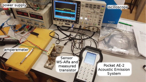
The measurement circuit consisted of an acoustic emission sensor of the alpha series from the Physical Acoustic Corporation, a portable recorder Pocket AE2 from MISTRAS; parallel recordings of changes were also made by a digital oscilloscope.
The calibration of the circuit was conducted with the Hsu-Nilsen source method (Figure ), breaking a pencil lead (0.5 mm dia 2H hardness) shielded by a suitably adapted tip placed in an automatic pencil. The head and the pencil protruding 3 mm ensures the same angle for each break, thus the same reproducible acoustic emission wave can be generated. Measurement of the signal obtained through the pencil lead break enables reproducible calibration of the measurement circuit.
Figure 2. Dimensions of the Hsu-Nilsen calibration head (Bejger Citation2012; ASTM Citation2015).
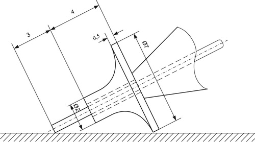
The transducer was placed on a smooth, ground steel plate. The pencil lead break takes place on the same surface at a distance of 50 mm from the transducer.
The duration of the signal was very short, so the spectrum of recorded vibrations approximately reflected the amplitude characteristics of the transducer and the whole circuit transferring the signal.
The tested semiconductor element was a single, 4th generation IGBT transistor IRG4PC40S. The most important parameters of the tested transistor are as follows: maximum collector-emitter voltage Vces = 600 V, collector–emitter voltage drop in conductive state of Vce(on) = 1.32 V and maximum collector current in conductive state for the temperature of the connector 25°C was Ic = 60 A. The transistor gate was controlled with rectangular shaped voltage of different frequencies, with a filling factor of 50%, generated by the generator JC5603P and converted by the optocoupler to a value of 10 V in off state and 0 V in on transistor state. With the use of the measurement system shown in Figure , it was possible to obtain any acoustic emission waveforms and signals of any type of transistor. The presented measuring system does not impose any limitations as to the number of tested single transistors, but in the present phase of the research, the possibility of testing transistor modules consisting of several semiconductor power elements enclosed in a common casing has not been checked yet.
Figure 3. Scheme of experimental rig used in switching transistor Q1 acoustic emission tests.
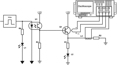
The laboratory test system contained only a transistor and an AE sensor placed directly on transistor’s heat sink. All other possible sources of acoustic emission signals coming from e.g. parasitic inductances were physically separated. During the measurements, devices containing inductances were moved away to such a distance that any interference from them was completely negligible. Due to the internal structure of the transistor, it was impossible to separate the signals coming from the charging of parasitic capacitance, which also gives background signal. This signal should be taken into account during the comparison process of properly working and damaged semiconductors.
The results
Considering the principles of bipolar transistors operation one can conclude that lower switching voltages on the IGBT transistor were obtained at the expense of switching speed, particularly switching off. Fast switching off characterises MOSFET transistors. The problem associated with IGBT transistors is that there is no possibility of carrying away hole carriers from the junction area. One way of accelerating the drainage of the accumulated charge is to feed inverted polarity voltage, which is not feasible. On the basis of preliminary studies carried out so far, it seems that changes can be observed using the AE signal (Figure ).
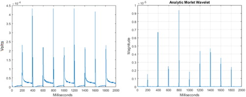
Figure 4. The signal of radiated AE elastic wave during the IGBT transistor switching, (left – time-voltage signal, right – amplitude-time signal). The measurements were made with a Pocket AE2, MISTRAS-made analyser (Physical Acoustic Corp.).
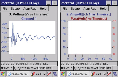
Figure presents a wave phenomenon (from Figure ), a source signal associated with ‘capturing’ the moment/phase of transistor transient period. In this particular case, the signal was recorded with the use of an AE measuring instrument designed at the Maritime University of Szczecin. For an analysis of frequency bands associated with an impulse from transistor switching, authors used the Morlet wavelet analysis (Figure ).
Figure 5. The source signal of the AE elastic wave (left) and its frequency analysis (right).
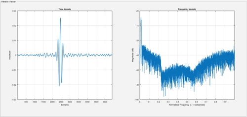
Figure 6. A wavelet analysis of acoustic emission from switching an IGBT transistor.
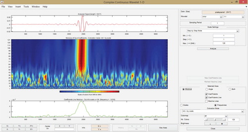
The spectrum of wavelet transform using the Morlet wavelet presented in Figure , offers an opportunity to obtain more accurate distribution of signal component frequency amplitudes. An extremum corresponding with transistor switch is clearly recognisable (Goldman Citation1999).
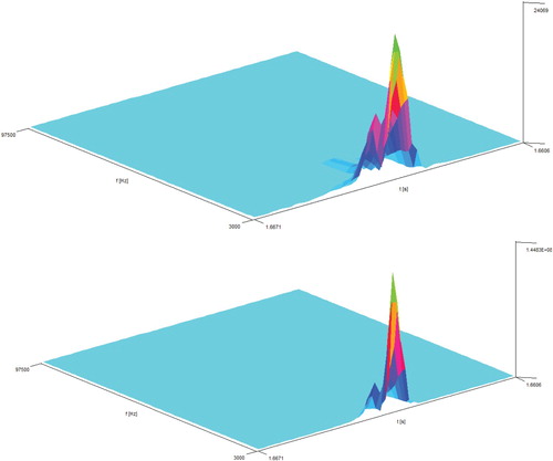
To check the temperature influence on the acoustic wave emission in the body of switching transistor some additional tests were performed. The transistor surface temperature was measured with infrared camera and the results showed there were no visible differences between signals coming out of 80°C and 96°C IGBT (Figures –).
Figure 7. The infrared camera display showing the temperature of tested transistor.
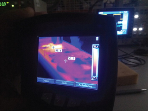
Figure 8. Results of wavelet analysis obtained at 80°C (raw signal from the AE sensor on the left, wavelet analysis result applied to the signal on the right).
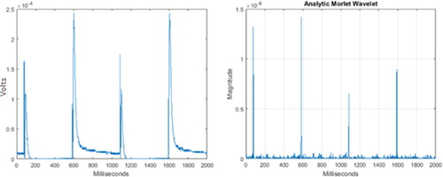
Figure 9. Results of wavelet analysis obtained at 96°C (raw signal from the AE sensor on the left, wavelet analysis result applied to the signal on the right).
Examining the propagation of AE elastic waves the ray theory is often used, in which each signal propagation path from the source to the point of observation is taken into account in electrodynamics equations.
During transistor switches, the function of amplitude changes at the AE source has a form of unit step (discrete step). Assuming that the elastic wave propagates in a homogeneous medium, the elementary equation describing the path of signal propagation in this form (Wang et al. Citation2009; Bejger Citation2012; Sause Citation2013; Bejger and Gawdzińska Citation2015) can be written as follows:
(1)
(1) where Gij (r, t′- t; r) are Green’s functions for the displacement in directions x′i, y′i, z′i at point r′ at instant t′ when those displacements are due to local disarrangement of the stress field at point r at instant t,
– density of the medium [kg/m3], vp – speed of dilatation wave, vS – speed of shear wave,
,
, for i = 1, 2, 3, j = 1, 2, 3, source-receiver and receiver-source directional cosines, r – distance between AE source and sensor,
– Kronecker delta,
– delta function equal to
for x = 0 and equal to 0 for the other values of x.
In practice, the receiver of AE signal (sensor) is located on the surface of the examined medium and at that point, it records the signal v(t). Based on an analysis of the v(t) form the properties of the signal sources or properties of the medium through which the signal is propagating can be concluded. In addition, to amplify the signal and filter out undesirable components (noises and disturbances), the analog signal has to be converted into a digital form, i.e. discrete in terms of value and in time domain, to be further processed. The discrete form of signal v can be represented as v(m). The index in brackets represents the discrete time variable identifying successive measured samples of the signal. The process of sampling is made at frequency f1, and its inverse – time interval between successive sample generation – T1 is the sampling period. T1 characterises the quality of analog–digital processing system. It should be recalled here that, if the measurement system converts an analog signal at sampling frequency f1, then it will be possible to distinguish in the discrete form of the signal only frequencies up to the maximum value f1/2 (Bejger Citation2012) by methods described further. The problem of reproducing the form of AE signal v(t) generated in the source is generally complex (Bejger Citation2012; Sause Citation2013). The method of conventional analyses of that signal consists in classifying the form of its changes as a function of time on the basis of voltage changes registered on the sensor. Different classifiers in use, called descriptors, are describing signal changes in time, signal energy changes or spectral components of the signal. In the present case, in addition to wavelet analysis, the authors used an analysis of power spectral density (PSD) (Figure ). The power spectral density describes how the power of a signal is distributed over frequency as the Fourier transform shows the spectral content of given signal i.e. the amplitude and phase of harmonics in the measured signal.
Figure 10. Analysis of the power spectral density of the AE signal during bipolar transistor switch.
The PSD analysis helps to isolate the most important harmonic components and to determine the magnitude of amplitudes of those components. The analysis determines amplitudes of subsequent harmonics (the amplitude spectrum) and/or phase shifts (phase spectrum). The random process of switching (or fault occurrence) of the transistor x(t), can be considered as a periodical process with the period tending to infinity T ∈ (−∞, +∞). For the signal interval specified, it cannot be represented by a complete series of Fourier transform because the following condition is not met (Sause Citation2013):
(2)
(2)
To fulfil this condition, it is not the process x(t) that is examined, but its autocorrelation function Rxx(τ). Such a procedure is feasible because the autocorrelation function Rxx(τ) contains information about the frequencies included in the tested signal. The function Rxx(τ) demonstrates a maximum when x(t) and x(t + τ) are in phase, and a minimum when they are in counter phase. With the assumption that the process x(t) was normalised by deducting from it the mean value and also assuming that x(t) has no periodic components, then:
(3)
(3) and the condition is fulfilled:
(4)
(4)
Therefore, the continuous Fourier transform to the analysis of Rxx(τ) can be applied. By transforming function x(t) defined in the time domain to the frequency domain ω, a complex function X(ω) can be obtained, i.e. continuous Fourier transform of x(t):
(5)
(5) and denoting this transform as Sx(ω) we get:
(6)
(6) Similarly, to the transform of the real signal x(t), this transform can be also represented on the plane of complex numbers and written in the following form:
(7)
(7) where
(8)
(8)
(9)
(9) Bearing in mind that the parity is a feature of the autocorrelation function and sin(ωτ) is an odd function, we get:
(10)
(10) and then:
This means that the continuous Fourier transform of the autocorrelation function Rxx(τ) has only the real component (unlike the transform of real signal x(t) which also has an imaginary component) and on the basis of Equation (8) it is even. The inverse transform can be expressed as:
(11)
(11)
For τ = 0 we get:
(12)
(12) and on the basis of the defining formula of the autocorrelation function true is following relationship:
(13)
(13)
This equation implies that the area under the curve Sx(ω) is equal to the mean square value of the stationary random process, so it expresses the signal power over the whole frequency band (Figures and ). The product Sx(ω)⋅dω denotes the power of signal component with circular frequency ω contained in the interval dω. The Fourier transform of autocorrelation function Sx(ω) is a continuous spectrum of the random signal power density in the frequency domain on the interval −∞ to +∞, and is called the bilateral spectral power density, often used in theoretical considerations. In practice, the concept of unilateral spectral power density Gx(ω), specified for the frequency interval 0 ≤ ω < +∞, is of more importance in the case under consideration. If the signal x(t) is a real function, the corresponding power density spectrum is a real even function, therefore, the unilateral power density function can be expressed as:
(14)
(14)
Replacing Sx(ω) = A(ω) from equation (8) we get:
(15)
(15)
Analysing the above considerations, it can be assumed that spectral density distribution of the signal associated with transistor switch (or signal change caused by a fault), allows identifying early fault conditions of the tested element.
Conclusions and future work
The article demonstrates the applicability of acoustic emission elastic wave signals for detecting the moment of switching, but primarily the correctness of work (switching) of an insulated gate bipolar transistor. It seems that the use of Morlet wavelet transform for signal analysis gives a good image of the distribution of frequencies characteristic of the examined process (Chao Citation2010). If changes in the internal transistor structure occur, new characteristic frequencies are generated (to be discussed in a separate article). At the same time, changes in the amplitude and nature of distribution of the signal power spectral density allow to specify internal (without having external symptoms) energy changes associated with impaired work of the transistor.
Disclosure statement
No potential conflict of interest was reported by the author(s).
ORCID
Artur Bejger http://orcid.org/0000-0001-5392-1979
Maciej Kozak http://orcid.org/0000-0002-0062-1590
Radosław Gordon http://orcid.org/0000-0001-6340-633X
Additional information
Notes on contributors
Artur Bejger
Artur Bejger, PhD Eng., is Professor at Maritime University of Szczecin. The fields of his research interests include diagnostics, maintenance and forecasting of machinery, equipment and technical systems. Throughout his work dealt with research related to the use of elastic waves of acoustic emission to identity condition called ‘Difficult to diagnose’ devices – mainly on ships. In addition, he developed his interests related to the repair and regeneration and installation of machinery. Research was verified in practice, as exemplified by many orders of scientific and industrial research, extensive cooperation with shipping companies and repair as well as publications presented in the form of papers, statements, and scientific conferences. He was proposing and finding effective methods to allow non-invasive diagnosis of the injection system for internal combustion engines using injection system failure information contained in the signal of acoustic emission of elastic waves.
Maciej Kozak
Maciej Kozak, PhD Eng., is Professor at Maritime University of Szczecin. The main research activity of the author is the control of power electronics systems used in power plants utilising variable speed generators. The topics of the interest is investigation of influence of the energy storage systems on the operation of the variable speed generators and the phenomena associated with uneven power distribution between DC–DC and AC–DC converters. One of the side areas of interest is the development of diagnostic methods using acoustic emission allowing early notification of possible semiconductor structures damage. The author directs research programme related to the study of acoustic emission phenomena in semiconductors of devices operating at medium voltage.
Radosław Gordon
Radosław Gordon, MSc. Eng. is Assistant at Maritime University of Szczecin. Currently working on his PhD thesis on Acoustic Emissions in Power Semiconductors. In this subject he is conducting research in the laboratory of ‘Green Energetics’ of Maritime Academy in Szczecin. He is also a lecturer of subjects related to electrical engineering and conducts laboratory classes in this field. He studies inverter devices and their influence on mechanical systems, e.g. higher harmonics on destruction of bearings in electric machines.
References
- Al’Akayshee Q, Neal H, Sartain A, Reynolds S, Yuan X, Al’Akayshee M. 2016. An 8 Mw, 3-level inverter drive based on press-pack IGBT’S: design, construction and operational propulsion system. 8th IET International Conference on Power Electronics, Machines and Drives PEMD. doi:10.1049/cp.2016.0254.
- ASTM. 1982. E610 – Standard Definition of Terms Relating to Acoustic Emission.
- ASTM. 2015. Document Number ASTM-E976-84, Standard Guide for Determining the Reproducibility of Acoustic Emission Sensor Response, 2015 EDITION – Determining the Reproducibility of Acoustic Emission Sensor - Jan. 1, 2016.
- Bejger A. 2012. Zastosowanie fal sprężystych emisji akustycznej do diagnozowania układów wtryskowych okrętowych silników spalinowych. FOTOBIT Kraków.
- Bejger A, Gawdzińska K. 2015. An attempt to use the coherence function for testing the structure of saturated composite castings. Metalurgija. 54(2):361–364.
- Berger A, Agostinelli M, Vesti S, Oliver JA, Cobos JA, Huemer M. 2015 Nov. A wireless charging system applying phase-shift and amplitude control to maximize efficiency and extractable power. IEEE Trans Power Electron. 30(11):6338–6348. doi: 10.1109/TPEL.2015.2410216
- Chao W. 2010. Gabor wavelet transform and its application.
- Chen W, Tao H, Lou L, Liu C, Cheng W, Tang X, Liu H, Zhou Q, Deng X, Li X, Zhang B. 2017. Low loss insulated gate bipolar transistor with electron injection (EI-IGBT). IEEE J Electr Devices Soc. 5(4):275–282. doi: 10.1109/JEDS.2017.2701791
- Choi U-M, Blaabjerg F, Lee K-B. 2015 May. Study and handling methods of power IGBT module failures in power electronic converter systems. IEEE Trans Power Electron. 30(5):2517–2533. doi: 10.1109/TPEL.2014.2373390
- Chybowski L, Wiśnicki B. 2015. Wybrane aspekty nauczania zasad eksploatacji okrętowych układów napędowych z prądnicami wałowymi (Selected aspects of teaching operation procedures for marine propulsion systems with shaft generators). Syst Wspomagania Inżynierii Produkcji Inżynieria Systemów Technicznych. 2:11.
- Diab HY, Marei MI, Tennakoon SB. 2016. Operation and control of an insulated gate bipolar transistor-based current controlling device for power flow applications in multi-terminal high-voltage direct current grids. ET Power Electron. 9(2):305–315. doi:10.1049/iet-pel.2015.0525.
- Goldman S. 1999. Vibration spectrum analysis. A practical approach. New York (NY): Industrial Press Inc.
- Harman GG. 1979. Non-destructive tests used to insure the integrity of semiconductor devices with emphasis on passive acoustic techniques. In: Zemel JN, editor. Nondestructive evaluation of semiconductor materials and devices. NATO advanced study institutes series (Series B: Physics). Vol. 46. Boston, MA: Springer. doi:10.1007/978-1-4757-1352-7_13.
- Holroyd T. 2000. Machine & systems condition monitoring series. acoustic emission & ultrasonics. Oxford: Coxmoor Publishing Company.
- Kärkkäinen T, Talvitie JP, Kuisma M, Hannonen J, Ström J-P, Silventoinen P. 2014. Acoustic emission in power semiconductor modules – first observations. IEEE Trans Power Electron. 29(11):6081–6086. doi: 10.1109/TPEL.2013.2295460
- Kärkkäinen TJ, Talvitie J, Kuisma M, Silventoinen P, Mengotti E. 2015. Acoustic emission caused by the failure of a power transistor. IEEE Applied Power Electronics Conference and Exposition (APEC): p. 2481–2484. doi:10.1109/APEC.2015.7104697.
- Khanna VK. 2003. Insulated gate bipolar transistor IGBT theory and design. Wiley. doi:10.1002/047172291X.
- Kim DE, Lee DC. 2009 Jun. Fault diagnosis of three-phase PWM inverters using wavelet and SVM. J Power Electron. 9(3):377–385.
- Kozak M, Gordon R, Bejger A. 2016. Control of squirrel-cage electric generators in a parallel intermediate DC circuit connection. Sci J Marit Univ Szczec. 45(117):17–22. doi:10.17402/080.
- Lee Y-C, Kim J-S, Yun Y-S, Jeon H-M. 2016. Analysis on thermal loss reduction on electric power propulsion system on board ship. IEEE Transportation Electrification Conference and Expo, Asia-Pacific (ITEC Asia-Pacific): p. 929–934. doi:10.1109/ITEC-AP.2016.7513084.
- Lu B, Sharma S. 2009 Sept.-Oct. A literature review of IGBT fault diagnostic and protection methods for power inverters. IEEE Trans Ind Appl. 45(5):1770–1777. doi:10.1109/TIA.2009.2027535.
- Mai-Khanh NN, Nakajima S, Iizuka T, Mita Y, Asada K. 2017. Experimental demonstration of non-destructive detection of IGBT fault positions by magnetic sensor. IEEE Sensors Applications Symposium (SAS): p. 1–4. doi:10.1109/SAS.2017.7894042.
- Peimankar A. 2013. Evaluation of partial discharge in power transformers by acoustic emission and propagation modeling of acoustic signal. Int J Electr Energy. doi:10.12720/ijoee.1.4.182-187.
- Salomonsson D, Sannino A. 2007. Low-voltage DC distribution system for commercial power systems with sensitive electronic loads. IEEE Trans Power Deliv. 22(3):1620–1627. doi: 10.1109/TPWRD.2006.883024
- Sause M. 2013. Acoustic emission signal propagation in damaged composite structures. J Acoust Emiss. 31.
- Sun P, Gong C, Du X, Peng Y, Zhou L. 2017 May. Condition monitoring IGBT module bond wires fatigue using short-circuit current identification. IEEE Trans Power Electron. 32(5):3777–3786. doi:10.1109/TPEL.2016.2585669.
- Tarnapowicz D. 2010. The conception of the use of multi-level inverters in the shipping shaft generator systems of high power. Sci J Marit Univ Szczec. 22(94):67–70.
- Trabelsi M, Boussak M, Mestre P, Gossa M. 2011. An improved diagnosis technique for IGBTs open-circuit fault in PWM-VSI-fed induction motor drive. 2011 IEEE International Symposium on Industrial Electronics; Gdansk, Poland. p. 2111–2117. doi:10.1109/ISIE.2011.5984487.
- Valentine N, Das D. 2016. Impact of dormancy periods on power cycling of insulated gate bipolar transistors (IGBTs). IEEE Accelerated Stress Testing & Reliability Conference (ASTR): p. 1–6. doi:10.1109/ASTR.2016.7762269.
- Wang XH, Shu CM, Mao HL, Huang ZF. 2009 Jan. Wavelet packet analysis for the propagation of acoustic emission signals across turbine runners. NDT E Int. 42(1):42–46. doi: 10.1016/j.ndteint.2008.07.005