Abstract
Square-shaped, single-crystal, monolayer graphene domains are grown on Cu foils by low-pressure chemical vapor deposition. The domains are remarkably well-aligned along the direction of flow of the gases. Scanning electron microscopy shows that these ‘square’ domains have clean, smooth edges which permit seamless, defect-free merging of the domains. Raman spectra and transmission electron microscopy together demonstrate that individual domains are single layer, and electron diffraction reveals that these domains are single crystals. The expansion mechanism of ‘square’ graphene domains is discussed in the context of our aligned, tailored domain shapes. This work represents an important step toward realization of fabrication of larger area, single-crystal monolayer graphene sheets with controllable shape and alignment.
Graphene growth by chemical vapor deposition (CVD) has enabled successful production of large-area graphene layers on copper (Cu) substrates, greatly encouraging the use of graphene in practical applications Citation1. However, the large-area synthetic graphene produced so far is typically polycrystalline Citation2–4, consisting of a number of small single-crystalline grains separated by grain boundaries Citation5–7. Multiple graphene grains of different in-plane orientations are simultaneously nucleated in random and uncontrolled locations on the surface of polycrystalline copper foils. As the growth proceeds, these graphene grains coalesce and eventually form interconnected polycrystalline films. Since the neighboring graphene domains formed at different copper grains have different orientations of carbon atom hexagonal lattices, it is challenging to connect atomically matched domains at the boundaries. The sizes of grains and the grain boundaries between them are predicted to strongly affect the electrical Citation3 Citation4 and mechanical Citation8 properties of graphene films. In fact, it is no secret that the best carrier mobility (∼200,000 cm2 V−1 s−1) Citation9 of graphene has come from layers peeled from rare natural graphite, while the CVD polycrystalline graphene shows a carrier mobility of a few hundred to a few thousand cm2/(V s) Citation1 Citation3 Citation10. Therefore, the initial nucleation and growth dynamics of graphene play a critical role in determining the final quality of CVD graphene films, and it is highly desirable to synthesize either large-area high-quality single-crystalline graphene films, or to achieve lower nucleation density of individual graphene grains so as to minimize the grain boundaries. However, merely controlling the nucleation number of graphene grains (also known as ‘domains’) is insufficient. The shape and structure of individual graphene domains also greatly influences its property and directly determines the grain boundary in polycrystalline graphene films. Thus, the tailoring and direct observation of the domain shape structure are very important for understanding the growth mechanism as well as to maximize single-crystalline graphene's inherent outstanding properties for future applications.
Studies on the dynamics of CVD graphene growth on copper foils have chiefly focused on the initial stages that show various interesting graphene domain shapes, such as hexagonal Citation11–13, six-sided polygon Citation10, fourfold-symmetric lobe Citation3 Citation14, rectangular Citation15 Citation16, and triangular Citation17. Robertson and Warner were among the first to grow hexagonal-shaped single-crystal domains of graphene on copper foils using atmospheric pressure (AP-CVD) Citation11. They found that the hexagonal structures have a six-fold symmetry, stemming from the crystal symmetry of graphene. Li et al. obtained a fairly large, six-sided polygon structured graphene domain of up to 0.5 mm in size in a copper foil enclosure by low-pressure (LP) CVD Citation10. Wu et al. studied the interaction between graphene domain shapes and high-purity (99.999%) copper foils by AP-CVD. They found that few-layer graphene has a rectangular structure on Cu grains with only (111) orientation Citation15, but hexagonal domain shapes on nearly all non-(111) Cu lattice planes. Liu et al. also studied the interplay of Cu foil and graphene by AP-CVD Citation17. They found the shape of graphene can be tuned to a structure of triangular domains by changing the Cu surface to a cubic (100) orientation. An annealing method to suppress the graphene nucleation on Cu foils has been recently published, in which square graphene domains characterized by jagged edges are obtained by AP-CVD Citation18.
In this paper, we report for the first time the growth of large-scale single-crystal ‘square’ graphene domains on Cu foils during the early stage of CVD operated under LP. The square graphene domains have orientations aligned with each other, and along the flow direction of reaction gases inside the LP-CVD. These square graphene domains as grown are continuous across Cu grain boundaries, but display wrinkle stripes with completely different orientations on opposite sides of a Cu boundary. The wrinkle stripes can disappear with the formation of cracks on the surface of square graphene domains. The edges of ‘square’ domains grown in the LP-CVD are smooth, in sharp contrast to the jagged edges formed in AP-CVD previously reported.
The conditions (please see the supplemental materials) used in this work for the synthesis of graphene were optimized to enable observation of the morphology of single domains and elucidate their growth mechanism. At the lower partial pressure of methane and higher partial pressure of hydrogen, separate graphene domains were obtained in most cases. shows scanning electron microscopy (SEM) images of graphene domains growing on the surface of Cu foils, with some of them growing across the boundaries between Cu grains. The graphene corresponds to the dark contrast areas shown in the SEM image. The dark areas consist of either a single domain or multiple coalesced domains. The Cu surface itself contains many features such as grain boundaries, annealing twins, and polycrystalline facets resulting from high temperature (1,035°C) processing (see the supplemental material ). The polycrystalline nature of the Cu foils is indicated by the change of contrast in the SEM image. The graphene domains are typically square, with ∼90° angles between adjacent edges. As illustrates, the domain edge directions parallel each other, and furthermore, the diagonal between top and bottom corners in all the square graphene domains appear to have an orientation very aligned with each other, which is the directional flow of reaction gases (indicated by red arrows, shown in ). This alignment implies that graphene hexagons can be seamlessly connected at the domain boundary as we shall demonstrate in the following sections. Cu foils mainly have Cu (100) facets with a square-shaped lattice Citation3 Citation14 Citation19 Citation20, suggesting a well-defined epitaxial relation between the shape of graphene domains and that of the underlying Cu grain lattice. However, a closer examination of the SEM image in reveals that the alignment is in fact independent of the polycrystalline Cu substrate which consists of multiple facets of different identities. Furthermore, the graphene domain density on the light contrast Cu grain is similar to that on the dark contrast Cu grain, suggesting no preferential nucleation on a particular Cu grain. This lack of correlation between the graphene crystal orientation and the underlying Cu substrate demonstrates a weak graphene–Cu interaction arising from weak van der Waals forces, and is in agreement with previous reports Citation11 Citation12 Citation21 Citation22.
Figure 1. Typical SEM images of ‘square’ graphene domains and the red arrow in the images indicating the reaction gases flow direction. (a, b) Low magnification. (c, d) High magnification. White spots in (b) and around the edges of the domains in (c) and (d) arise from copper nanoparticles.
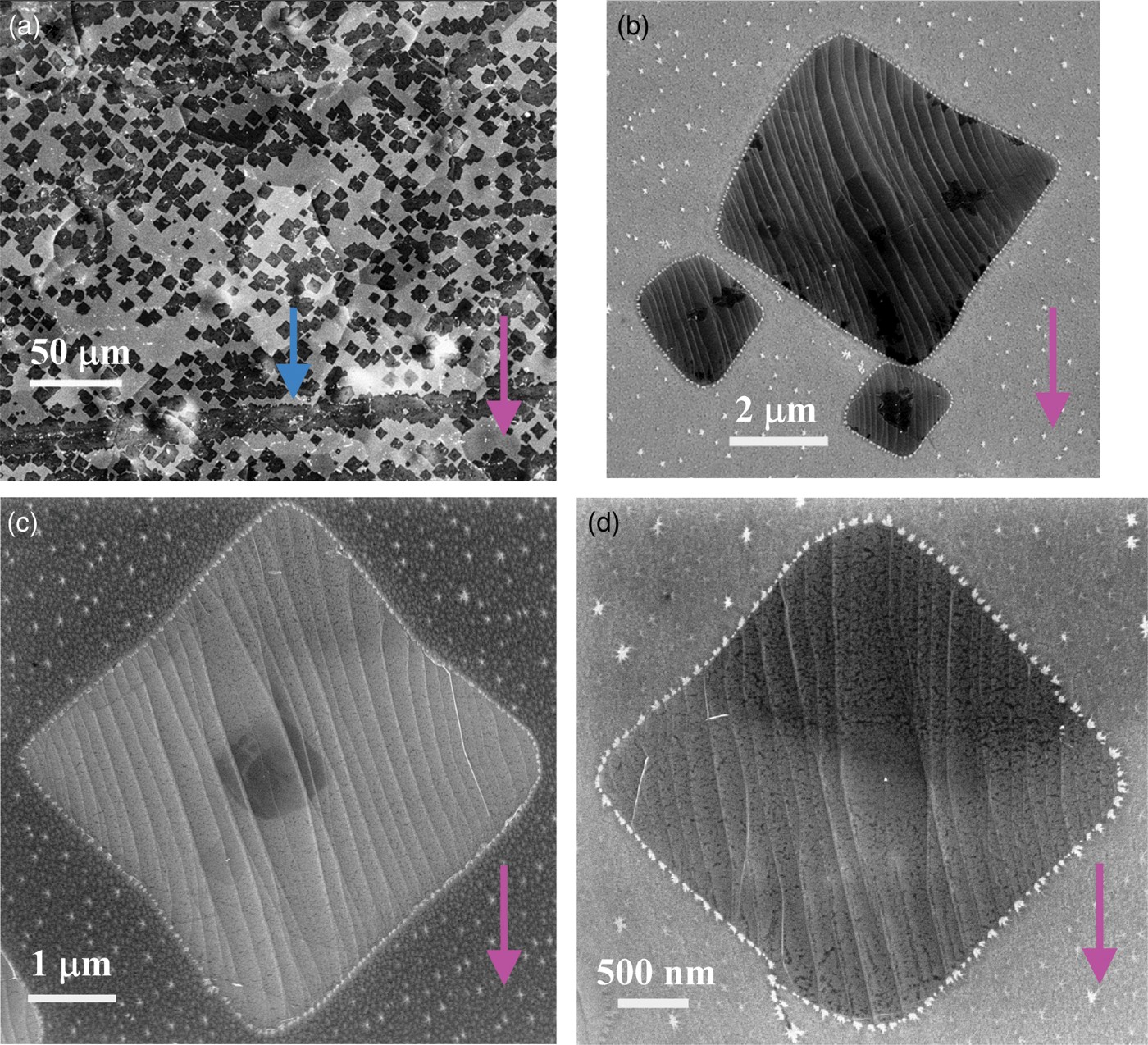
shows several graphene domains in a Cu grain, showing the same crystal orientation and the size change of domains. The size differences between the domains seen in , suggest that not all domains nucleate and grow simultaneously. The smaller graphene islands have just started to nucleate, while the others have already grown to larger domains. In general, the nucleation and growth of the graphene domains on Cu substrate are determined by the saturation of active C species derived from the decomposition of methane Citation3, which is dependent on the methane partial pressure at a fixed growth temperature. On the other hand, considering that the total flow rate of about 500 sccm is relatively high, it is possible that the reaction gases in the LP-CVD are in a state of turbulence, and so it is hard to achieve a uniform distribution of C species in the entire oven tube in a given short reaction time of about 2 min. Thus, it is possible that while graphene domains grow simultaneously, some grow to a certain size, and then growth ceases because the amount of the local C species available is not sufficient in the condition of low saturation. In contrast, local supersaturated C species on the exposed Cu surface can contribute to the formation of the graphene stripes consisting of many coalescing square domains (indicated by a blue arrow in ).
The higher-magnification SEM images showing two graphene domains with sizes of 4.5×4.5 μm2 and 2.3×2.3 μm2 are presented in and , respectively. shows that an additional top flake can grow on the graphene surface; while shows a pure, ‘square’ graphene domain with a very smooth edge. Such smooth edges facilitate the formation of larger domains by seamless merging compared to jagged edges Citation18. It is possible that the growth of additional top flakes occurs only at the beginning Citation11 Citation23, where the local amount of C species available exceeds what can be consumed by the square-shaped graphene domains. Careful examination of the four sides of graphene domain edges reveals many bright, white dots, which are Cu/oxide nanoparticles. In fact, we found that almost every square domain has nanoparticles on the edge, and the nanoparticles are regularly spaced along the sides of the edge. Energy-dispersive X-ray spectroscopy gives a strong Cu-peak and the absence of any other elements (see the supplemental material ). Most of the ‘square’ domains have a dimension of up to about 9×9 μm2, which give a growth rate of approximately 4.5 μm/min or an area growth rate of 40.5 μm2/min, while the minimum ‘square’ domain in our observations is 500×500 nm2 in size.
Figure 2. Typical high-magnification SEM images of ‘square’ graphene domains. (a) A ‘square’ graphene domain across the curved Cu grain boundary (blue arrows). (b) SEM image showing the difference in the directions of wrinkle stripes in the crossing point of three Cu grain boundaries. (c, d) Individual square graphene domains with wrinkles or cracks.
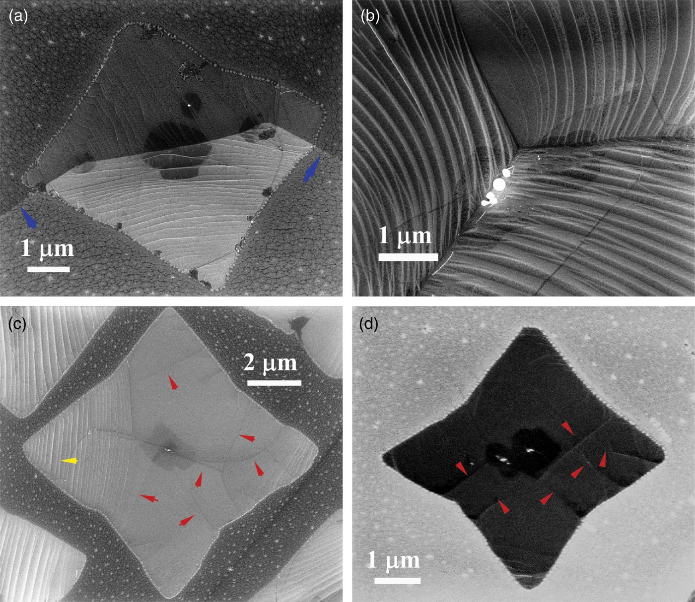
shows high-magnification SEM images of graphene domains growing across copper grain boundaries (indicated by two blue arrows in ), thereby confirming that graphene domains are weakly coupled to the underlying Cu surface. Closer examination of the surface of the square domain () reveals that the parallel directions of the wrinkle stripes are completely different on either side of the curved Cu grain boundary, where wrinkle stripes in the top half have a vertical parallel direction and wrinkles with a slightly bright contrast in the bottom half orient along the horizontal direction. The difference in the directions of wrinkle stripes is more clearly evident in , which shows the crossing point of three Cu grain boundaries. In general, two-dimensional (2D) membranes have a tendency to be crumpled to minimize the total free energy. Graphene is no exception and wrinkles are encountered on the surface of almost all graphene samples grown by CVD using metal substrates Citation24 Citation25. Graphene domains become compressively stressed in the cooling process, due to the mismatch in the thermal expansion coefficients of graphene and the substrate. Finally, graphene domains locally delaminate and form such one-dimensional wrinkles. Our observations indicate that the wrinkle structures are dependent on the underlying Cu grain orientations; different Cu in-plane orientations lead to different directions of graphene wrinkles. This is the first direct experimental evidence for the role of the underlying in-plane orientations of the Cu grain in the determination of parallel wrinkle stripe directions in a graphene domain.
These wrinkles can be locally stretched out when cracks are created within graphene. shows that part of the wrinkle stripes in the square graphene domain have disappeared due to the formation of crack lines (red arrows) to relieve local strain. If enough cracks are created in graphene, then the thermally induced strain will be completely relaxed. As illustrates, the wrinkle stripes in the ‘square’ graphene domain have been almost completely stretched out due to the existence of many cracks (red arrows). In fact, the wrinkle formation can be reversed by heating up again, which has been reported previously Citation25. It has been argued that wrinkling limits the thermal Citation26 and electric Citation27 conductivities of graphene. However, the formation of these wrinkles might not necessarily be a drawback depending on application. The wrinkling of graphene can be engineered to produce graphene nanoribbons Citation28 and can prevent graphene sheets from restacking and thus increase active surface area for graphene application in energy storage devices such as supercapacitors Citation29.
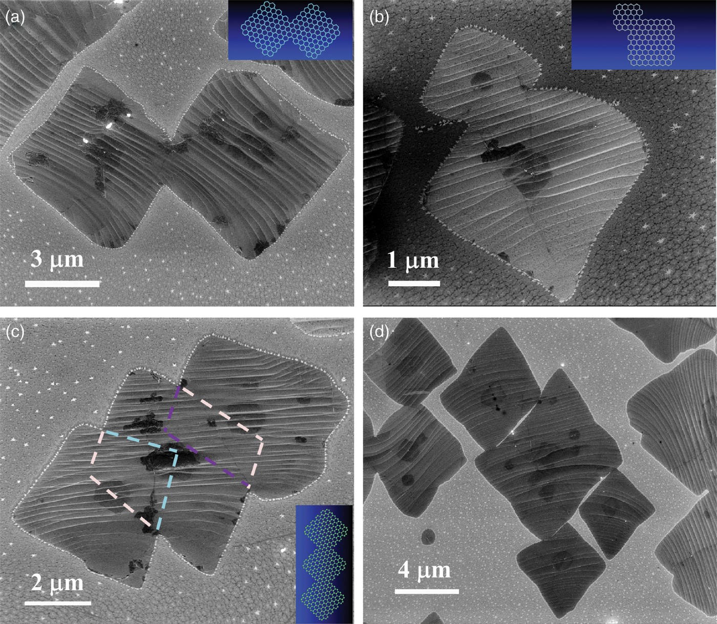
The observations on merging domains can provide very important information about how graphene can be grown to obtain larger domains. and shows the merging of two ‘square’ domains ( with almost the same dimensions and 3(b) with domains of different sizes). If graphene nucleation locations are close enough, then the front edges can merge together to grow into larger domains, forming a continuous sheet. As illustrates, three domains have merged together early in the growth process and then continue to grow while retaining their individual square-shaped features (dashed lines). The merging process is illustrated through models shown as insets in –(c), respectively. Square-shaped graphene domains merge together not only at sharp corners (–(c)) but also through their wide sides. shows the beginning stages of several ‘square’ domains coalesced together from their wide sides. The wrinkle stripes exhibit the same parallel direction within their merging large domains, respectively. However, it is possible that very thin overlapping sheets would also show the same ripple structure. Furthermore, there are no additional graphene flakes and no apparent defects in these merging areas, which are smooth and similar to other parts of the domains. These observations suggest that ‘square’ graphene domains seamlessly merge with each other to form larger domains, which will be confirmed by Raman spectroscopy as shown below.
Figure 3. Typical high-magnification SEM images of coalescing square graphene domains: two merging graphene domains with (a) same and (b) different sizes, respectively. (c) Three coalescing graphene domains. (a–c) Insets showing their models, respectively. (d) Multiple graphene domains merging through corners and sides, respectively.
To verify the layer number of graphene domains and evaluate the quality and presence of defects in graphene, Raman spectra were recorded under ambient conditions with a 632.8 nm (1.96 eV) wavelength excitation laser and a 50× objective lens was used to focus the excitation laser light spot of approximately 1–2 μm on the graphene samples. Because most of our graphene domains have a lateral size of about 9 μm, they are visible under the Raman 50× objective lens. Furthermore, Cu is oxidized in air after several days, while the areas covered by the graphene domains are well protected from oxidation and appear to be whiter and brighter areas as compared to the dark yellow Cu. It should be mentioned that no contrast is seen except for Cu grain boundaries in the optical images if Raman measurements are performed right after LP-CVD growth of graphene. shows an optical image with many visible graphene domains, where a domain is surrounded by yellow Cu particles and form a clear square shape in the center of this image (indicated by a dashed square box). As we described in the SEM images as above, the four sides of each square domain have many Cu nanoparticles attached and these nanoparticles are much easier to be oxidized than bulk Cu and appear as deeper yellow contrasts in optical images.
Figure 4. (a) Optical image of individual square graphene domains by Raman microscopy with a 50×objective lens. (b) Corresponding Raman spectra showing single-and multi-layer graphene on specific regions of the Cu surface as indicated by a dashed box and a blue arrow in (a). (c) Optical image of coalescing graphene domains by Raman microscopy with a 50×objective lens. (d) Corresponding Raman spectra showing single-layer graphene in merging regions as indicated by yellow arrows in (c).
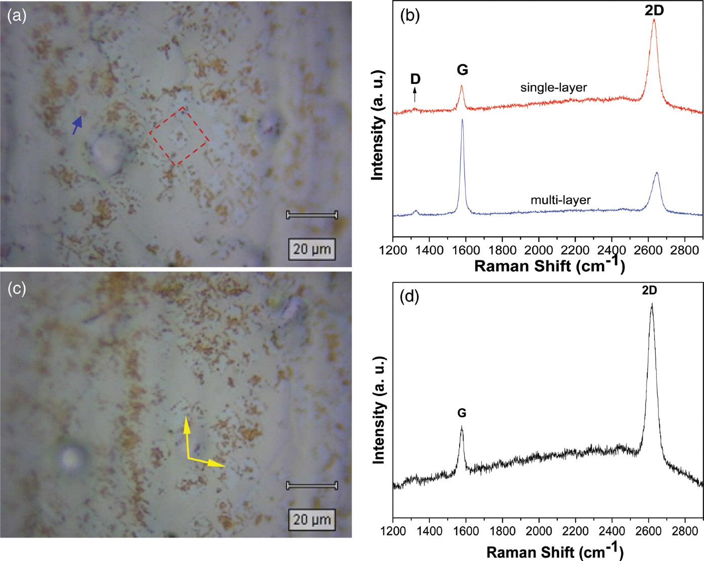
The typical Raman spectrum (the red line in ) from white and bright graphene domains consists of two main peaks: G (∼1,581 cm−1) and 2D (∼2,644 cm−1). The intensity ratio of I 2D/I G is about 3.5 and the 2D-peak line width of FWHM (full width at half maximum) is ∼41 cm−1, indicating that the square domains are single-layer graphene Citation1. The intensity of disorder-induced D-peak (∼1,328 cm−1) is negligibly small, indicating the high quality of graphene. This suggests that wrinkles (in the SEM images) do not play an apparent role in the intensity of D-peak, implying the wrinkling of graphene is non-defective. In fact, the wrinkle formation can be reversed by heating, which was already reported previously Citation25. The small D-peak shows disorder in the localized areas of the graphene and is probably induced by cracks or large Cu particles. As the blue line in illustrates, the Raman spectrum from the additional top graphene flakes with big Cu particles (blue arrow in ) shows a multi-layer feature with defects, where I 2D/I G is 0.45 and I D>/I G is 0.05. This confirms what has been observed by SEM. shows an optical image with many visible coalescing graphene domains. In numerous measurements across merging areas of different coalescing square domains, the observed Raman spectra display almost the same characteristic peaks as that of single-layer graphene domains () without sign of remarkable defects (D-peaks). A typical Raman spectrum from the merging spots (yellow arrows in ) is shown in , in which has no significant D-peak detected and I 2D/I G ratio is also about 3.5, indicating the non-defect-merging of these square graphene domains. This finding suggests that coalescing domains are seamlessly connected to each other to form larger and continuous graphene sheets, which is in good agreement with the SEM observations as above.
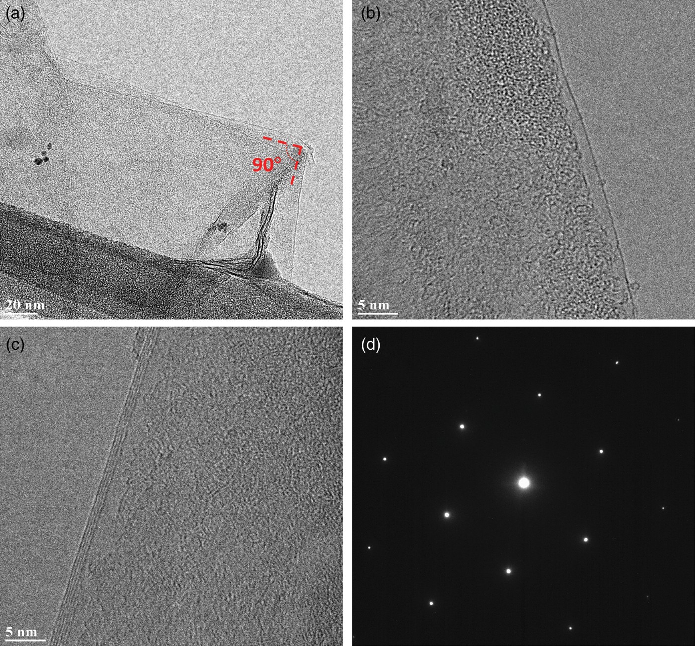
High-resolution (HR) TEM (transmission electron microscopy) was performed on graphene samples that were transferred to lacey copper grids with amorphous carbon films. shows a low magnification TEM image of folded graphene film edges with ∼ 90° corners (indicated by dashed red lines), demonstrating the square shape of the graphene domains. It should be mentioned that the transfer process causes the graphene sheets of atomic thickness to be folded or torn or broken. Polymethyl-methacrylate residues (black dots) arising from the transfer process are also seen in Citation12. All of these impediments limit our ability to obtain TEM images of the whole square feature on individual graphene domains. Nevertheless, the monolayer feature of square graphene domains is easily revealed in the edges of sheets. A typical TEM image is presented in , indicating that the graphene is single-layered. This confirms the result of the monolayer by Raman characterizations. As shown in SEM images, additional top flakes are frequently observed in domains including edges, and this is also confirmed by TEM (), indicating a multi-layer feature of three to five layers. shows a set of sixfold-symmetric electron diffraction spots in a selected area, indicating that the observed domain is a single crystal. But inherent constraints in the transfer process limit our ability to probe the single-crystal nature of the coalescing domains. However, based on the TEM observations and Raman analysis, we can conclude that individual ‘square’ domain is single-layer graphene.
Figure 5. HRTEM images of (a) the edges of single-layer graphene domains with ∼90° corners (indicated by dashed red lines). (b) Single-layer graphene. (c) Few-layer graphene. (d) Electron diffraction showing single-crystal structure feature of individual ‘square’ graphene domains.
The CVD growth of graphene on Cu occurs via surface nucleation and 2D domain expansion. The growth of hexagonal graphene domains has been explained on the basis of a growth mechanism that is dominated by the sixfold symmetry of the graphene lattice with little influence from the underlying Cu substrate Citation11–13. The formation of other graphene domains such as the four-lobed, triangle, and rectangle domains is attributed to the in-plane features of the Cu substrate Citation3,Citation14–17. However, the square structure of our graphene domains is dissimilar to these shapes. The 100 facet of Cu is known to be a structure with square lattice Citation3 Citation14 Citation19 Citation20, suggesting that it catalyzes the formation of ‘square’ graphene domains. However, the polycrystalline nature of our Cu foils with multiple different facets and different in-plane orientations coupled with our observation of ‘square’ graphene domains growing on such a polycrystalline surface would rule out the influence of the underlying Cu substrates in our case. From this microscopic evidence, we construct a probable ‘square’ graphene domain expansion scenario.
It is well-known that the hexagonal-shaped graphene domains can be bounded by only zigzag or only armchair edges Citation30, which are shown in . However, both zigzag and armchair edges must together contribute to the formation of a ‘square’ graphene domain. In other words, if one edge is zigzag, then the adjacent edge must be armchair edge in a ‘square’ graphene domain (). As can be seen from the high-magnification SEM images in , each side of the square has many Cu nanoparticles attached. To investigate the role of these Cu nanoparticles on growth of graphene, we performed a blank experiment without the addition of methane, where other experimental conditions are exactly the same as that of graphene growth. The growth temperature of graphene in the isothermal zone of the LP-CVD reactor can reach as high as 1, 035°C, (only 48°C lower than the melting point of Cu, 1, 083°C), suggesting that the copper atoms have a high degree of mobility at the surface and thus leading to the formation of a thin melting layer close to the surface Citation17 Citation31. The highly mobile Cu atoms contribute to the formation of a large number of Cu nanoparticles. SEM images obtained from blank Cu foils subjected to the LP-CVD process in the absence of methane are shown in –(d).
Figure 6. (a) Schematic models showing hexagonal shapes with only zigzag, only armchair edges, and a square shaped domain with both zigzag and armchair edges on sides. (b) Typical SEM image of the Cu surface showing the Cu grain boundaries and Cu nanoparticles. (c, d) High-magnification SEM images showing a big Cu particle, dendrite-like Cu nanoparticles, and rough Cu surface morphologies.
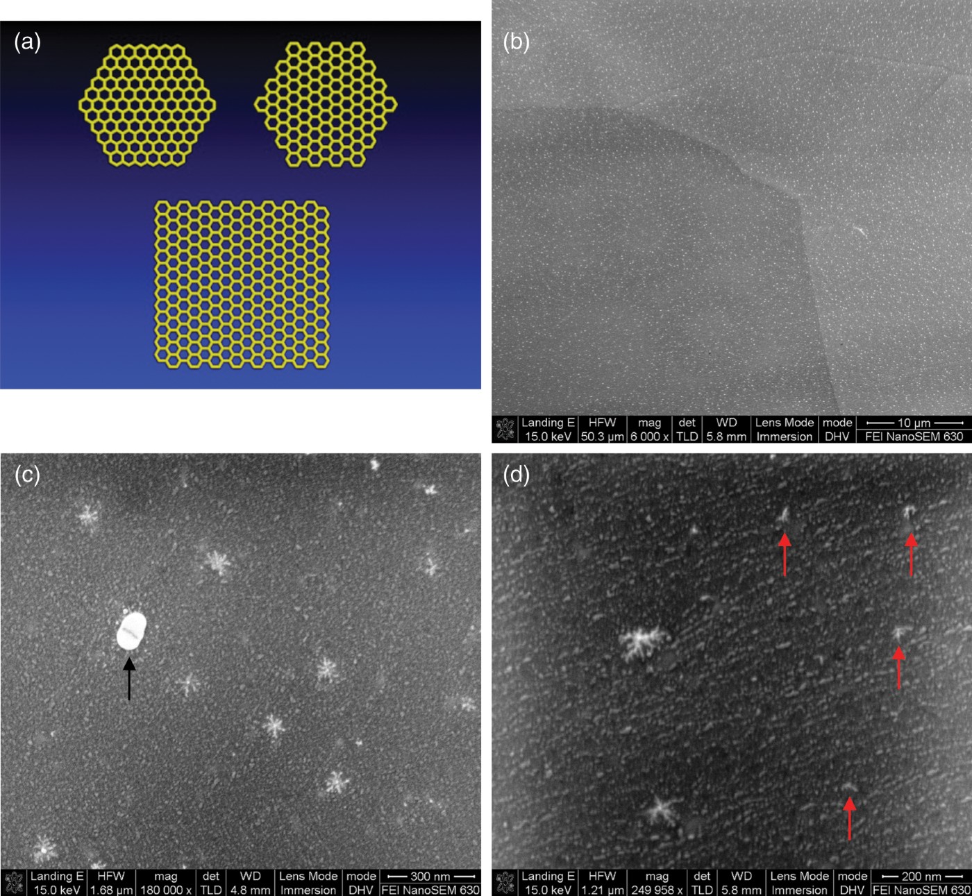
As indicates, the Cu nanoparticles are uniformly distributed and appear as small white dot contrasts in the SEM image, where Cu grain boundaries are also clearly seen with different contrasts, suggesting that the formation of nanoparticles is independent of the Cu grain facets. shows that some smaller dendrite-like Cu nanoparticles (red arrows) may be growing during the annealing of Cu foils (also see supplemental material ). Dendrite structural growth from a stable cluster is common for particles growing following a homogeneous nucleation process. It is in fact suggesting a rather weak interaction of these Cu clusters and particles with the substrate. The Cu surface exhibits a rough morphology with a lot of small protrusions due to pre-treatments of Cu foils by diluted (2%) HNO3. It is possible that these small protrusions on the surface of rough Cu foils not only favor the formation of these dendrite-like Cu nanoparticles, but also benefit the nucleation of graphene. Theoretical calculations have shown that the formation energy on Cu is almost the same for the zigzag and armchair edges, i.e. neither edge is apparently preferred Citation30. Hexagonal-shaped graphene growth is known to occur with edges dominated by the zigzag direction. This is because monomer attachment to armchair edges is energetically favored and hence armchair edges of graphene domains can be converted into a zigzag geometry which in turn enables the growth of zigzag edges to yield hexagonal graphene domains Citation30. However, in the case of ‘square’ graphene domains, the surrounding Cu nanoparticles on their four sides provide stable binding sites for adatoms (due to the formation of Cu-C). Adatom attachment to any edge including armchair-zigzag boundaries is energetically stable and favored in the same way. The strong affinity of carbon atoms to self-assemble and expand the sp2 lattice drives the symmetrical growth of graphene on the Cu surface in both edge directions of zigzag and armchair, respectively. Thus, square graphene domains with both zigzag and armchair edges are maintained, while the slight distortions of some square domains may be attributed to the impurities (such as big Cu particles) or rougher features of the Cu surface. However, the initiation process for ‘square’ graphene is still unclear, and requires consideration of multiple factors, e.g.: hydrogen flow rate and its role, flow dynamics (attributing to the alignment), pressure and temperature in LP-CVD reactor, the role of the underlying Cu in the beginning of square graphene nucleation, and the methane flow rate. This will need further investigation, but it is clear that ‘square’ graphene domains are observed under our growth conditions with a high hydrogen partial pressure. Hydrogen may affect the catalytic efficiency and plays a role in controlling the size and morphology of graphene domains, which has been reported previously Citation23.
In summary, we have shown that aligned ‘square’ single-layer graphene domains with smooth edges can be synthesized on polycrystalline Cu foils by CVD operated in LP. The monolayer nature of the ‘square’ domains is confirmed by Raman spectroscopy and TEM, and the alignment is found to be along the flow direction of reaction gases. The growth of ‘square’ graphene domains do not appear to be influenced by the underlying Cu, while different Cu in-plane orientations play an important role on the wrinkle stripe parallel directions in a graphene domain. The aligned ‘square’ graphene domains have a lateral dimension of up to several micrometers; and with modified growth conditions, the results presented above could pave the way to fabrication of larger area monolayer graphene sheets.
Supplementary online material
A more detailed information on experiments is available at http://dx.doi.org/10.1080/21663831.2013.772078.
Acknowledgements
We thank the NSF CREST award HRD-0833184 for financial support of this research (G-PD, KV, DKT, and MHW). Grant DMR-0959679 provided support for SEM images. Partial funding for MHW was provided by the NASA URC award NNX09AV07A. The authors thank the UNC Energy Frontier Research Center for the use of the Raman system. The assistance of Dr AS Kumbhar (HRTEM measurements) Nanofab. Lab., UNC at Chapel Hill is also greatly appreciated.
References
- Li , X , Cai , W , An , J , Kim , S , Nah , J , Yang , D , Piner , R , Velamakanni , A R , Jung , I , Tutuc , E , Banerjee , S K , Colombo , L and Ruoff , R S . 2009 . Large-area synthesis of high-quality and uniform graphene films on copper foils . Science. , 324 : 1312 – 1314 . (doi:10.1126/science.1171245)
- Liu , Y and Yakobson , B I . 2010 . Cones, pringles, and grain boundary landscapes in graphene topology . Nano Lett. , 10 : 2178 – 2183 . (doi:10.1021/nl100988r)
- Li , X , Magnuson , C W , Venugopal , A , An , J , Suk , J W , Han , B , Borysiak , M , Cai , W , Velamakanni , A , Zhu , Y , Fu , L , Vogel , E M , Voelkl , E , Colombo , L and Ruoff , R S . 2010 . Graphene films with large domain size by a two-step chemical vapor deposition process . Nano Lett. , 10 : 4328 – 4334 . (doi:10.1021/nl101629g)
- Yazyev , O V and Louie , S G . 2010 . Electronic transport in polycrystalline graphene . Nature Mater. , 9 : 806 – 809 . (doi:10.1038/nmat2830)
- Huang , P Y , Ruiz-Vargas , C S , van der Zande , A M , Whitney , W S , Levendorf , M P , Kevek , J W , Garg , S , Alden , J S , Hustedt , C J , Zhu , Y , Park , J , McEuen , P L and Muller , D A . 2011 . Imaging grains and grain boundaries in single-layer graphene: an atomic patchwork quilt . Nature. , 469 : 389 – 392 . (doi:10.1038/nature09718)
- Kim , K , Lee , Z , Regan , W , Kisielowski , C , Crommie , M F and Zettl , A . 2011 . Grain boundary mapping in polycrystalline graphene . ACS Nano. , 5 : 2142 – 2146 . (doi:10.1021/nn1033423)
- An , J , Voelkl , E , Suk , J W , Li , X , Magnuson , C W , Fu , L , Tiemeijer , P , Bischoff , M , Freitag , B , Popova , E and Ruoff , R S . 2011 . Domain (grain) boundaries and evidence of “twinlike” structures in chemically vapor deposited grown graphene . ACS Nano. , 5 : 2433 – 2439 . (doi:10.1021/nn103102a)
- Grantab , R , Shenoy , V B and Ruoff , R S . 2010 . Anomalous strength characteristics of tilt grain boundaries in graphene . Science. , 330 : 946 – 948 . (doi:10.1126/science.1196893)
- Bolotin , K I , Sikes , K J , Jiang , Z , Klima , M , Fudenberg , G , Hone , J , Kim , P and Stormer , H L . 2008 . Ultrahigh electron mobility in suspended graphene . Solid State Commun. , 146 : 351 – 355 . (doi:10.1016/j.ssc.2008.02.024)
- Li , X , Magnuson , C W , Venugopal , A , Tromp , R M , Hannon , J B , Vogel , E M , Colombo , L and Ruoff , R S . 2011 . Large-area graphene single crystals grown by low-pressure chemical vapor deposition of methane on copper . J Am Chem Soc. , 133 : 2816 – 2819 . (doi:10.1021/ja109793s)
- Robertson , A W and Warner , J H . 2011 . Hexagonal single crystal domains of few-layer graphene on copper foils . Nano Lett. , 11 : 1182 – 1189 . (doi:10.1021/nl104142k)
- Yu , Q , Jauregui , L A , Wu , W , Colby , R , Tian , J , Su , Z , Cao , H , Liu , Z , Pandey , D , Wei , D , Chung , T F , Peng , P , Guisinger , N P , Stach , E A , Bao , J , Pei , S S and Chen , Y P . 2011 . Control and characterization of individual grains and grain boundaries in graphene grown by chemical vapour deposition . Nature Mater. , 10 : 443 – 449 . (doi:10.1038/nmat3010)
- Wu , W , Jauregui , L A , Su , Z , Liu , Z , Bao , J , Chen , Y P and Yu , Q . 2011 . Growth of single crystal graphene arrays by locally controlling nucleation on polycrystalline Cu using chemical vapor deposition . Adv Mater. , 23 : 4898 – 4903 . (doi:10.1002/adma.201102456)
- Wofford , J M , Nie , S , McCarty , K F , Bartelt , N C and Dubon , O D . 2010 . Graphene islands on Cu foils: the interplay between shape, orientation, and defects . Nano Lett. , 10 : 4890 – 4896 . (doi:10.1021/nl102788f)
- Wu , Y A , Robertson , A W , Schäffel , F , Speller , S C and Warner , J H . 2011 . Aligned rectangular few-layer graphene domains on copper surfaces . Chem Mater. , 23 : 4543 – 4547 . (doi:10.1021/cm201823s)
- Liu , W , Li , H , Xu , C , Khatami , Y and Banerjee , K . 2011 . Synthesis of high-quality monolayer and bilayer graphene on copper using chemical vapor deposition . Carbon. , 49 : 4122 – 4130 . (doi:10.1016/j.carbon.2011.05.047)
- Liu , J , Wu , J , Edwards , C M , Berrie , C L , Moore , D , Chen , Z , Maroni , V A , Parans Paranthaman , M and Goyal , A . 2011 . Triangular graphene grain growth on cube-textured Cu substrates . Adv Funct Mater. , 21 : 3868 – 3874 . (doi:10.1002/adfm.201101305)
- Wang , H , Wang , G , Bao , P , Yang , S , Zhu , W , Xie , X and Zhang , W J . 2012 . Controllable synthesis of submillimeter single-crystal monolayer graphene domains on copper foils by suppressing nucleation . J Am Chem Soc. , 134 : 3627 – 3630 . (doi:10.1021/ja2105976)
- Wood , J D , Schmucker , S W , Lyons , A S , Pop , E and Lyding , J W . 2011 . Effects of polycrystalline Cu substrate on graphene growth by chemical vapor deposition . Nano Lett. , 11 : 4547 – 4554 . (doi:10.1021/nl201566c)
- Ogawa , Y , Hu , B , Orofeo , C M , Tsuji , M , Ikeda , K , Mizuno , S , Hibino , H and Ago , H . 2012 . Domain structure and boundary in single-layer graphene grown on Cu(111) and Cu(100) films . J Phys Chem Lett. , 3 : 219 – 226 . (doi:10.1021/jz2015555)
- Gao , L , Guest , J R and Guisinger , N P . 2010 . Epitaxial graphene on Cu(111) . Nano Lett. , 10 : 3512 – 3516 . (doi:10.1021/nl1016706)
- Vanin , M , Mortensen , J J , Kelkkanen , A K , Garcia-Lastra , J M , Thygesen , K S and Jacobsen , K W . 2010 . Graphene on metals: a van der Waals density functional study . Phys Rev B. , 81 : 081408 – 11 . (doi:10.1103/PhysRevB.81.081408)
- Vlassiouk , I , Regmi , M , Fulvio , P , Dai , S , Datskos , P , Eres , G and Smirnov , S . 2011 . Role of hydrogen in chemical vapor deposition growth of large single-crystal graphene . ACS Nano. , 5 : 6069 – 6076 . (doi:10.1021/nn201978y)
- Chae , S J , Gunes , F , Kim , K K , Kim , E S , Han , G H , Kim , S M , Shin , H J , Yoon , S M , Shin , H J , Yoon , S M , Choi , J Y , Park , M H , Yang , C W , Pribat , D and Lee , Y H . 2009 . Synthesis of large-area graphene layers on poly-nickel substrate by chemical vapor deposition: wrinkle formation . Adv Mater. , 21 : 2328 – 2333 . (doi:10.1002/adma.200803016)
- Hattab , H , N'Diaye , A T , Wall , D , Klein , C , Jnawali , G , Coraux , J , Busse , C , van Gastel , R , Poelsema , B , Michely , T , Meyer zu Heringdorf , F J and Horn-von Hoegen , M . 2012 . Interplay of wrinkles, strain, and lattice parameter in graphene on iridium . Nano Lett. , 12 : 678 – 682 . (doi:10.1021/nl203530t)
- Chen , S , Moore , A L , Cai , W , Suk , J W , An , J , Mishra , C , Amos , C , Magnuson , C W , Kang , J , Li , X and Ruoff , R S . 2011 . Raman measurements of thermal transport in suspended monolayer graphene of variable sizes in vacuum and gaseous environments . ACS Nano. , 5 : 321 – 328 . (doi:10.1021/nn102915x)
- Pereira , V M , Castro Neto , A H , Liang , H Y and Mahadevan , L . 2010 . Geometry, mechanics, and electronics of singular structures and wrinkles in graphene . Phys Rev Lett. , 105 : 156603 – 156606 . (doi:10.1103/PhysRevLett.105.156603)
- Pan , Z , Liu , N , Fu , L and Liu , Z . 2011 . Wrinkle engineering: a new approach to massive graphene nanoribbon arrays . J Am Chem Soc. , 133 : 17578 – 17581 . (doi:10.1021/ja207517u)
- Yan , J , Liu , J , Fan , Z , Wei , T and Zhang , L . 2012 . High-performance supercapacitor electrodes based on highly corrugated graphene sheets . Carbon. , 50 : 2179 – 2188 . (doi:10.1016/j.carbon.2012.01.028)
- Luo , Z , Kim , S , Kawamoto , N , Rappe , A M and Charlie Johnson , A T . 2011 . Growth mechanism of hexagonal-shape graphene flakes with zigzag edges . ACS Nano. , 5 : 9154 – 9160 . (doi:10.1021/nn203381k)
- Rasool , H I , Song , E B , Allen , M J , Wassei , J K , Kaner , R B , Wang , K L , Weiller , B H and Gimzewski , J K . 2011 . Continuity of graphene on polycrystalline copper . Nano Lett. , 11 : 251 – 256 . (doi:10.1021/nl1036403)