Abstract
Bimetal interfaces hold the extraordinary potential to promote or suppress deformation twinning in nanostructured composites. This article constructs a methodology for developing maps for identifying the twinnability of chemically sharp, bimetal interfaces based on their structure and properties. The map is shown capable of rationalizing the variation in experimental observations among several different bimetal interface structures.
Deformation twinning is one of the few basic mechanisms that face-centered cubic (fcc) metals Citation1–3 employ to plastically accommodate an applied mechanical force. For single-phase fcc metals, there has been widespread interest in understanding the nucleation and growth of deformation twins and establishing guidelines for determining which materials can twin and when and where in the material twins form Citation4 Citation5. The appearance of twins can be correlated to applied conditions, such as low temperatures and/or high strain rates, in which the thermodynamic processes that underlie slip dislocation motion become difficult Citation6 Citation7, or to material areas experiencing high localized stress concentration, such as near surfaces or cracks Citation8 Citation9. Also playing a role are chemical and physical material properties, such as the intrinsic stacking fault energy, other maxima and minima on generalized planar fault energy (GPFE) curves, alloying, and crystallographic orientation Citation1 Citation6,Citation10–13. Within suitably oriented fcc crystals, twinning occurs more readily in metals with a low stacking fault energy (SFE), such as Ag (intrinsic SFE γ=16 mJ/m2 Citation14) than those with an intermediate SFE, such as Cu (γ=45 mJ/m2 Citation15) or a high SFE, like Al (γ=122 mJ/m2 Citation2). In addition to the above, as grain sizes reduce to the nanoscale, grain size becomes an important factor in the promotion of deformation twins, and twins originate from grain boundaries Citation4 Citation10,Citation16–19. Within the nanoscale range, an optimal grain size has been observed, below which twinning becomes more difficult with decreasing grain size Citation20 Citation21. However, when deformation twins originate from bimetal interfaces, observations vary widely, from completely suppressed twinning Citation22 to fine twins with numerous twin boundaries (TBs) Citation23 Citation24 to fully twinned structures with no visible TBs Citation25 Citation26. The prior guidelines outlined above cannot rationalize the complete lack of twinning in 30 nm Cu within rolled nanolayered physical vapor deposition (PVD) Cu–Nb composites Citation22 or profuse twinning in submicron Cu within Cu–Ag composites rolled at elevated temperatures Citation25. These contradictions point to a need to revise twinning guidelines when considering two-phase materials. In this letter, we present an approach for developing a twinnability map for twinning from bimetal interfaces based on the interface structure. The interfaces considered here are sharp, exhibiting no chemical variation. All the above-mentioned conditions for deformation twinning still apply (suitable GPFE, crystal orientation relative to an applied stress, grain size and high stresses and/or rates), but are not sufficient without account of the structure of the interface.
When two crystals, differing in lattice parameters and/or in crystal structure, are joined, the relaxed equilibrium structure of the common interface that forms has an atomic structure that is unlike that of either crystal Citation27–30 (–(h)). The resulting interface can adopt a coherent structure (containing no intrinsic interface dislocations) or a semi-coherent structure (containing discrete interface dislocations) or an incoherent structure (often a disordered structure, in which discrete interface dislocations cannot be identified). Because coherent and incoherent interfaces do not have preferred nucleation sites for lattice dislocations, we focus on semi-coherent interfaces in the present work. Semi-coherent interfaces possess a well-defined, ordered atomic pattern, described as a regular network of discrete interface dislocations Citation30–32 (Figure S1). The network contains n arrays of discrete interfacial dislocations (i), i=1, …, n (see , where n=2). The number n of distinct arrays, their Burgers vectors B (i) and spacing S (i) for a given interface can be calculated using a combination of atomic-scale simulation (–(e)) and analytical methods described in Citation31–33 (Table 1 in supplement).
Figure 1. (a) Despite high rates and fine nanoscale thick layers, the interface on the left ((b) KS {111}| | {110}) does not form twins. Only the Cu–Nb interface structure in the center (labeled {112}| | {112}) forms twins in the upper Cu crystal Citation34. (c) Higher magnification of a typical twin in (a). High-resolution TEM micrograph of a typical (b) KS {111}<110>Cu| | {110}<111>Nb interface showing that it is atomically flat and (d) {112}<111>Cu| | {112}<110>Nb interface showing that it is faceted.
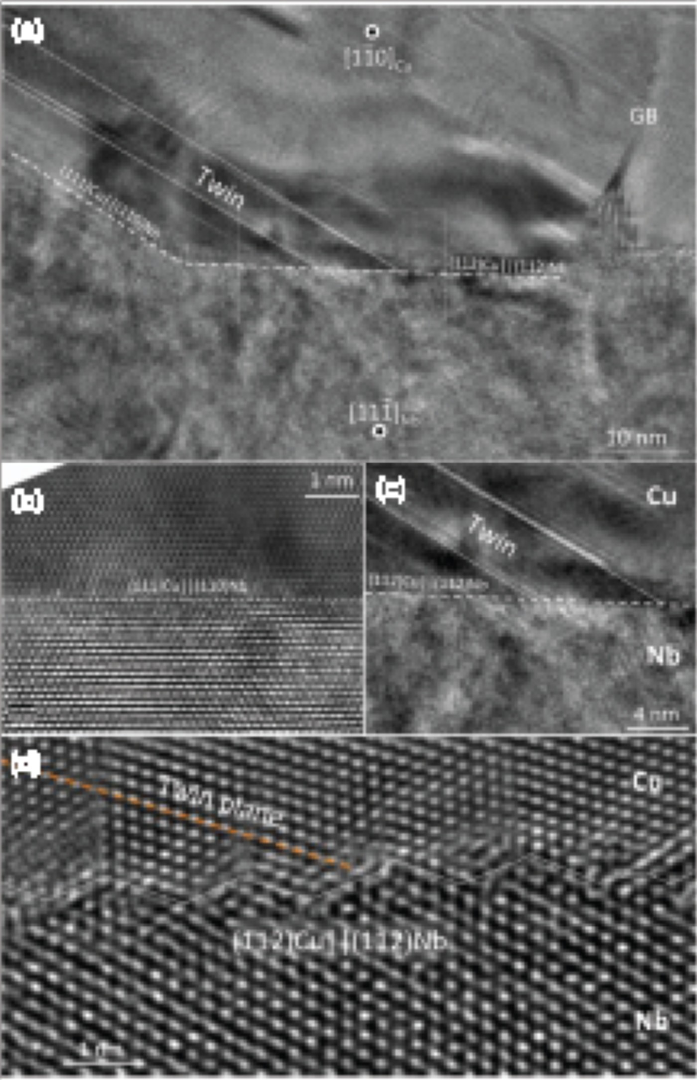
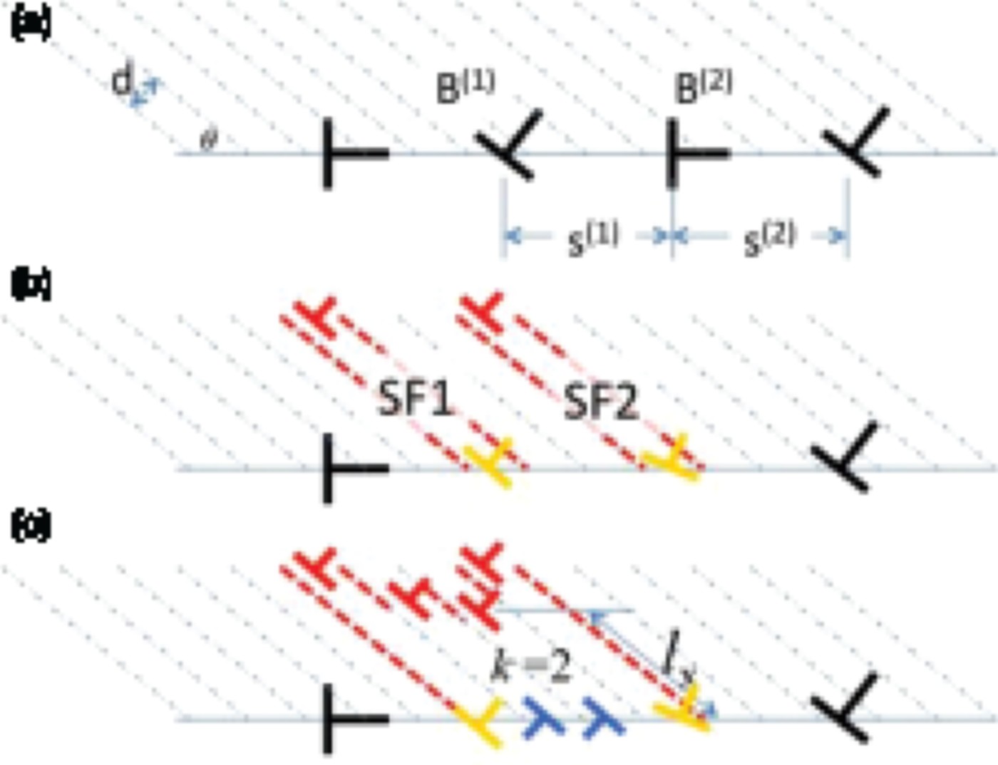
Figure 2. Illustration of twin nucleation directly from an interface due to its intrinsic structure. (a) A distribution of interface dislocations. Two sets are shown, each with a different total Burgers vector B
(1) and B
(2). Both sets have a Burgers vector component that is non-planar to the interface ( and
, respectively, although these components are not explicitly marked). (b) Dissociation of two interface dislocations, each into a residual and a TD that extends into the upper crystal. The TD forms a stacking fault as it glides. The two neighboring stacking faults, SF1 on the left and SF2 on the right, are spaced a distance s apart that equals the spacing of the two dissociation sites. The number of twin planes encompassed by s is equal to k. (c) Nucleation of k=2 TDs in between SF1 and SF2. As the k TDs glide away from the interface, they form a twin domain between SF1 and SF2. For a discussion on calculating k, please see supplement and Figure S2.
Within this class of semi-coherent interfaces lies a rich set of structures, not all of which can twin. The strong influence of interface structure is evident in , which displays a transmission electron microscopy (TEM) micrograph of a shocked Cu–Nb sample Citation34, wherein the semi-coherent interface in the center formed twins (), but those on the left did not. The corresponding high resolution TEM (HRTEM) micrographs of this area shows that the twinned interface was {112}⟨ 111⟩ Cu| | {112}⟨110⟩Nb, which is a faceted interface (), while the untwinned interface was {111}⟨ 110⟩ Cu| | {110}⟨ 111⟩ Nb, an atomically flat one (). Observations of twins from the former interface as well as other semi-coherent faceted interfaces are shown in –(c).
For the twinnability of these semi-incoherent interfaces, two mechanisms for successive emission of twinning dislocations (TDs) are considered. TDs can be emitted from an intrinsic interface dislocation or from an extrinsic interface dislocation. The former ‘intrinsic’ mechanism can involve, for instance, a non-planar dissociation of an intrinsic dislocation Citation35
Citation36. Should this be the dominant mechanism, the faceted interface ( and 1) would be favored over the atomically flat one. The former interface has interface dislocations with in-plane and out-of-plane Burgers vectors, i.e. , which could supply both Burgers vector components needed for a TD, unlike the flat interface, which only contains interfacial dislocations with in-plane Burgers vectors, i.e.
(). The latter ‘extrinsic’ mechanism can be identified as an interface slip–twin transmission event, wherein a glide dislocation (an extrinsic dislocation) runs into the interface from the adjoining crystal, and finally emits into the fcc crystal as a TD Citation29
Citation37
Citation38. The mapping methodology proposed below aims to predict the potential of a bimetal interface structure to act as a source of TDs via these two basic mechanisms for TD emission.
The first is referred to here as the dissociation (or D) mechanism. Under a mechanical driving force, TDs can emit directly from the interface via either dissociation of an interfacial dislocation Citation30 or indirectly from local stress concentrations generated around the interfacial dislocations Citation39. The D mechanism that we consider hereinafter corresponds to the former, since its activation barrier is much lower than that for the latter and hence is the more likely of the two to initiate the twinning process.
Twin formation via the D mechanism is proposed to proceed in two steps. In the first step , a TD is produced via dissociation of an interfacial dislocation, prompted by stress. Dissociation reactions should obey a few constraints, e.g. see Citation36, one of which translates here to a repulsive interaction between the residual dislocation left at the interface and the TD. In addition, energetically favored dissociation reactions are also those that reduce the net Burgers vector content of the interface; therefore, the residual dislocation should be smaller than the original interfacial dislocation. With these preliminaries, interface dislocations satisfying both energetic considerations tend to be those that have an out-of-plane component , which is larger in value than that of the TD b. In other words, an interface dislocation (i) satisfying
Interface dislocations within a region of high stress and satisfying EquationEquation (1) can dissociate into stacking faults spaced s
(i) apart (). Here, s
(i) defines the spacing between dislocation i and its adjacent neighbor dislocation j. The spacing s
(i) can be defined between two neighboring
in the i-array or two distinct but adjacent
and
, such as stacking faults SF1 and SF2 in .
The second step entails forming a twin domain that spans s (i), the distance between SF1 and SF2, via the nucleation of a TD on every twinning plane within s (i). If k planes lay in-between then k TDs need to nucleate (). When k equals one, then nucleation is spontaneous and a three-layer twin will form Citation17, but when k is too large, then twinning via the D mechanism is not possible. (The stacking faults SF1 and SF2 behave instead as individual partials, from which twinning by other mechanisms have been proposed Citation4 Citation20.) Whether or not the needed k TDs can nucleate can be determined via the following energetic expression for the change in energy due to the nucleation of k TDs:
The maximum value of G in EquationEquation (5) is G
0=0.25 The most effective pathway offered by the interface is associated with the highest value of G among all possible α–β pairs, denoted as G
max. In the calculation of G and G
max, we used θc=15° and ψc=45° Citation41. Geometrically efficient pathways can be expected to have a value of G
max≥0.0156 (or G
max/G
0≥0.0625), which corresponds to good geometric alignment
and large Schmid factors, each 0.25. Interfaces in which all favored pathways connect to the same twin plane (N=1), such as the {112}⟨ 111⟩ fcc| |{112}⟨ 110⟩ bcc interface (), present an instability that favors twin nucleation and thickening. Some interfaces may present more than one favorable dislocation transmission pathway (2≤N≤4). Unlike the case of N=1, multiple pathways (2≤N≤4) can potentially stabilize the adjoining crystal and hinder instabilities such as twinning (–(c)). We account for this effect later.
Figure 3. Transmissibility map for bimetal interfaces. Interfaces lying in the region near the origin are not as likely to permit slip–twin transmission and those lying away are more likely. Other areas marked ‘difficult’ correspond to regimes where slip–twin transmission would be difficult, but not impossible, requiring high stresses or high temperatures. Some experimental points are shown as ellipses. In these cases, interfaces from which twins form are colored in black and those from which they do not are colored in blue. Other experimental points are shown as rectangles due to the anisotropy in their interfacial shear strength (ISS). The ISS can be highly anisotropic, depending strongly on the direction of in-plane shearing Citation27 Citation30. In such cases, like the KS or NW interface, it is appropriate to report a range of τISS values, while for mildly anisotropic ones, reporting a single value suffices.
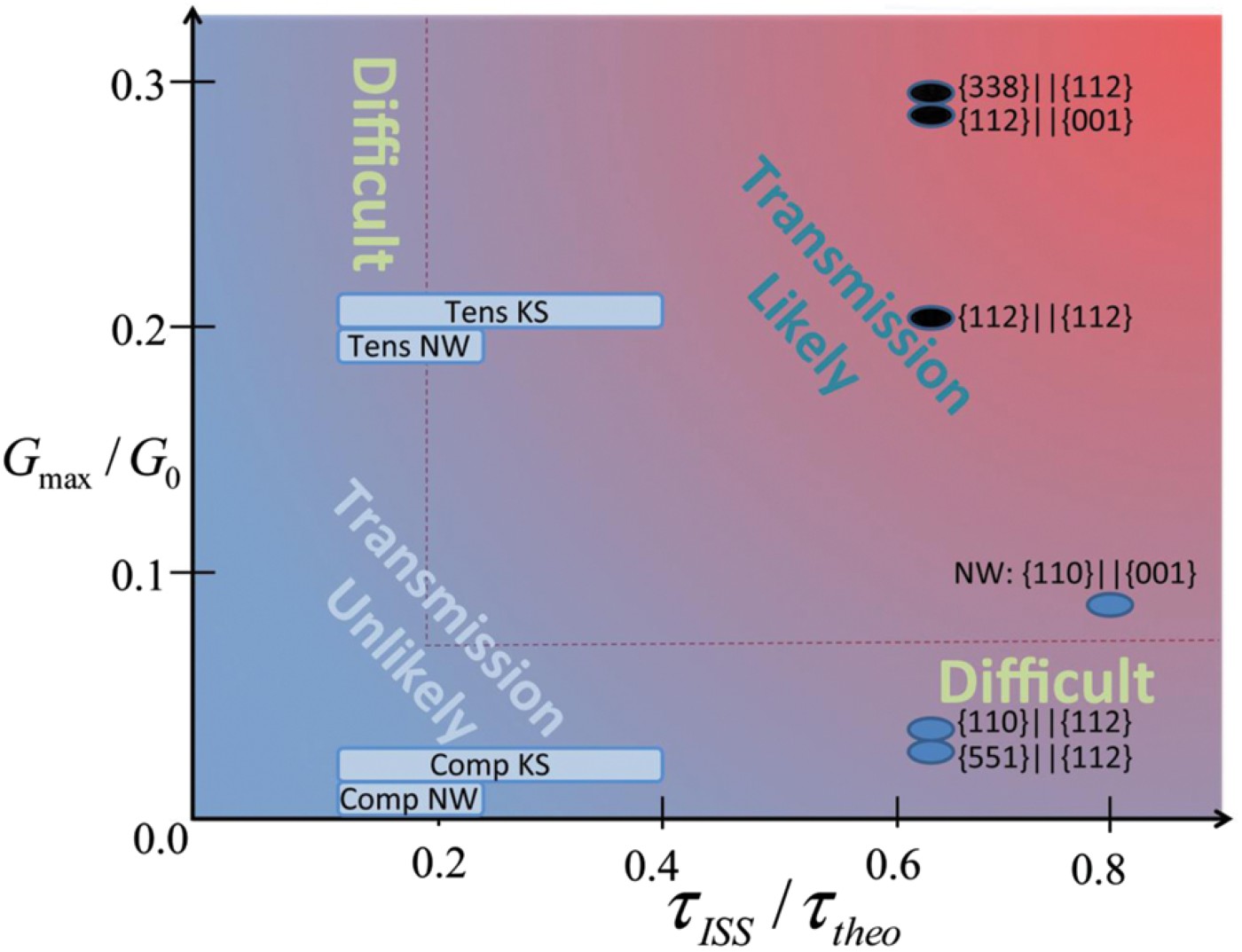
For demonstration, we apply the above measures to Cu–Nb interfaces deformed in plane strain compression normal to the interfaces (unless stated otherwise). Cu is the fcc metal in which twin formation is questioned and Nb is the bcc metal to which it is joined. To remove the influence of grain size in this example, we consider samples in which the individual Cu layers are one-grain thick and nanometer in scale. We begin with semi-coherent interfaces found in two Cu–Nb experimental systems that vary significantly in their intrinsic atomic structure as a result of differences in fabrication history. Set 1: Cu–Nb multilayers with nanoscale thicknesses (h<100 nm) fabricated by accumulative roll bonding (ARB), which are dominated by {112}⟨ 110⟩ Cu| |{112}⟨ 111⟩ Nb interfaces within 10° Citation42 ( and 1(a) and (c)). Set 2: Cu–Nb multilayers with nanolayer thicknesses fabricated by PVD, which develop thermodynamically equal portions of Kurdjumov–Sachs (KS) and Nishiyama–Wasserman (NW) interfaces Citation42 Citation43 (). These have been also found to be mechanically stable with strain, provided starting layer thicknesses are less 100 nm Citation44.
The tendency for transmission can be determined by mapping interfaces on a 2D plot of τISS/τtheo vs. G max/G 0, such as in . The τISS is normalized by its upper limit, the theoretical shear strength τtheo, and G by G 0=0.25. In this map, interfaces that would lead to twinning via the T mechanism must exhibit both high τISS/τtheo (no core spreading) and high G max/G 0 (geometrically effective pathway(s), ≥0.0625) and hence lie in the upper right-hand region. We apply the map in to a few experimental observations of twinned (black) and non-twinned (blue) interfaces, using τtheo=2.6 GPa for Cu and values for τISS from atomic-scale simulation (Table 1 in the supplement). Considering twin formation via the T-mechanism alone, twinning can be associated with interfaces with a large value of χ=(τISS/τtheo)(G max/G 0)/N, where N is the number of effective transmission pathways. Having N=1 such as in promotes a dynamic instability that favors twinning, whereas multiple pathways (N>1) such as in –(c) would not.
The propensity as well as the mechanism for twinning can be determined with the TD source map on , where one coordinate is related to the D mechanism and the other to the T mechanism χ from . The boundary S max=1 marked in corresponds to the limit below which twin formation via the D mechanism alone is not possible.
Figure 4. Twinnability map for bimetal interfaces. Interfaces lying in the region near the origin are not likely to twin and those lying away are more likely to twin by the T or D or both mechanisms. Regions where twinning occurs predominantly by the D or the T mechanism are also indicated. The figure-of-merit for the T-mechanism (x-axis) accounts for the number of effective transmission pathways, χ=(τISS/τtheo)(G max/G 0)/N (see Figure S3). Experimental points are shown as ellipses. Interfaces from which twins are observed to form easily and often are colored in black and those from which they did not are colored in blue. All cases are for compression or plane strain compression applied normal to the interface plane. The diamond symbols indicate predictions. NW and KS interfaces are predicted not to form twins when a tensile load is applied normal to the interface.
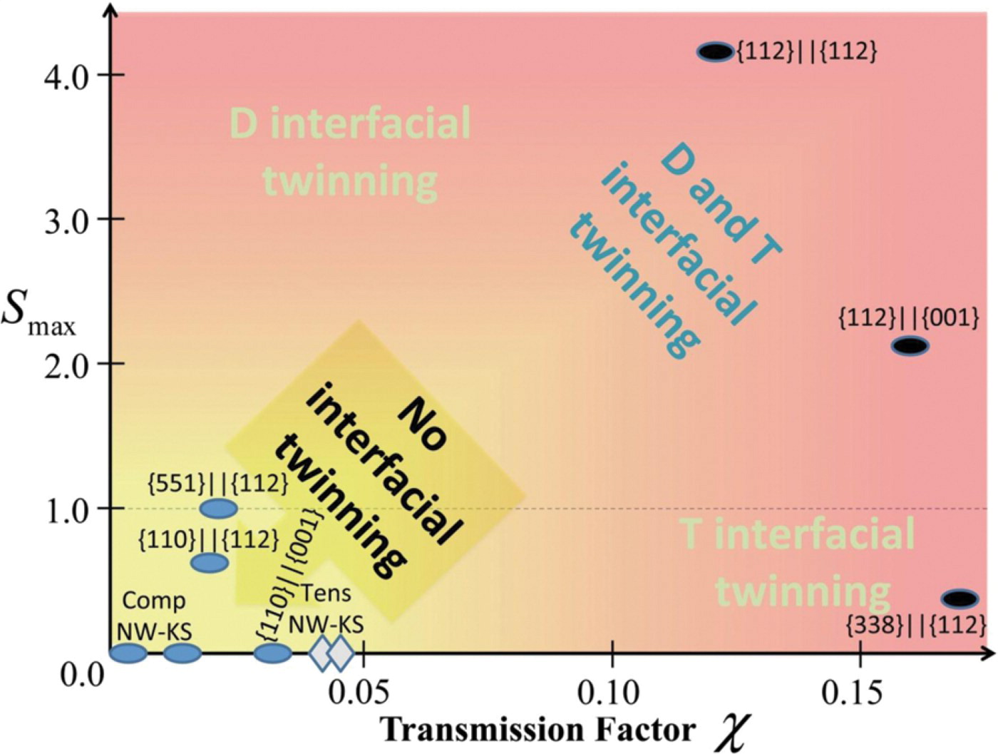
The map is designed such that twinning is unlikely for interfaces that lie close to the origin of this map, where the possibilities of operating the D and T mechanisms are low. As confirmation, interfaces in which twinning was not observed (blue points) collect in the ‘no-twinning’ region of the map. Two of these are the KS and NW interfaces, which are found in PVD nanolayered composites. Studies show that no twins are observed from these interfaces, regardless of layer thickness (even down to 5 nm), strain level, and strain rate (from quasi-static rolling to gas gun to laser shock Citation22 Citation34). In all these tests, the samples were compressed normal to the interfaces. The map indicates that if these interfaces were loaded instead in normal tension (diamonds), they still would not twin.
The propensity for twinning becomes more favorable with distance away from the origin. Twinning is especially likely for interfaces falling in the upper right-hand region of the map, where both the D and T mechanisms are favored. One interface that belongs to this twinning class is the {112}⟨ 111⟩ Cu| | {112}⟨ 110⟩ Nb interface, which has been reported in many studies to produce twins on a particular twin plane Citation23 Citation45 (). Significantly, twins in layers as large as 200 nm are observed to form from these interfaces Citation26. The map indicates that this interface uses both D and T mechanisms to nucleate and expand twins on the same twin plane. Another interface found in the Set 1 composites was the faceted {338}⟨ 443⟩ Cu| | {112}⟨ 110⟩ Nb interface, corresponding to an energy cusp in the formation energy landscape Citation32 (). Substantially less twins have been associated with this interface (). Its placement on the map suggests that it twins predominantly by the T-mechanism.
We utilize this map to predict the twinnability of other interfaces. We begin with interfaces occurring less frequently in the Set 1 material, such as the faceted {112}⟨ 111⟩ Cu| |{001}⟨ 110⟩ Nb interface (). The map predicts that this interface can twin using both D and T mechanisms. In agreement, we observe that twins are just as likely to form from {112}Cu| |{001}Nb interfaces (). Next we consider another set of ARB material, Set 3, with extremely fine nanoscale thicknesses (h≤20 nm), and different predominant interfaces, e.g. {551}⟨ 1 1 10⟩ Cu| |{112}⟨ 111⟩ Nb interface and the {110}⟨ 001⟩ Cu| |{112}⟨ 111⟩ Nb interface Citation26. Twins are not often observed from these interfaces. According to the map in , they are not expected to twin. As a last example, we examine a fourth set of Cu–Nb nanolayers (h≤30 nm) formed by rolling the Set 1 samples transversely, forming mainly an atomically flat {110}⟨ 111⟩ Cu| |{001}⟨ 110⟩ Nb interface. Twin formation was not associated with this interface (). This interface lies in the no-twinning region of the map since it is atomically flat (no D mechanism) and it favors dislocation transmission on multiple pathways (high N), which favors crystal stability and hinders instabilities, such as twinning (or shear banding).
The primary role of the twinnability map proposed here is to determine whether or not a given interface structure under a prescribed stress state can successively emit TDs. For sufficiently fine nanostructures, this critical nucleation step can be correlated with a measure twinning propensity. The map reveals the structural features controlling twinning and the type of twinning mechanism they drive. To date, it has been the only successful way to rationalize seemingly inconclusive observations on nanolayered composites. The map adds, and does not replace, an essential factor to previously established guidelines for twinning in fcc metals. To isolate the effects of interface structure from layer size h, strain rate and temperature, we fixed the latter set of variables. All experimental observations used for validation had nanoscale layer thicknesses (100 nm<h<10 nm). Like the leading partial, interface structure is also suspected to govern nucleation of the trailing partial, possibly giving rise to interface-structure-dependent grain-size effects. Size effects will be considered in future extensions of the map. The framework introduced here is suitably fundamental and can be applied to other bimetal interfaces involving different crystal structures, e.g. fcc/fcc and fcc/hcp. Bimetal interface twinnability maps can open the way to tuning bimetal interfaces to govern the relative activities of slip and twinning, the key to controlling microstructural evolution and material response under deformation.
Supplementary online material.
More detailed information on the theory and experiments are available at http://dx.doi.org/10.1080/21663831.2013.782074.
Acknowledgements
The authors gratefully acknowledge support by the Center for Materials at Irradiation and Mechanical Extremes, an Energy Frontier Research Center funded by the U.S. Department of Energy, Office of Science, Office of Basic Energy Sciences under Award Number 2008LANL1026.
References
- Christian , J W and Mahajan , S . 1995 . Deformation twinning . Prog Mater Sci. , 39 : 1 – 57 . (doi:10.1016/0079-6425(94)00007-7)
- Hirth , J P and Lothe , J . 1982 . “ Theory of dislocations ” . New York : Krieger .
- Venables , J A . 1964 . The nucleation and propagation of deformation twins . J Phys Chem Solids. , 25 : 693 – 700 . (doi:10.1016/0022-3697(64)90178-7)
- Zhu , Y T , Liao , X Z and Wu , X L . 2012 . Deformation twinning in nanocrystalline materials . Prog Mater Sci. , 57 : 1 – 62 . (doi:10.1016/j.pmatsci.2011.05.001)
- Meyers , M A , Vohringer , O and Lubarda , V A . 2001 . The onset of twinning in metals: a constitutive description . Acta Mater. , 49 : 4025 (doi:10.1016/S1359-6454(01)00300-7)
- Cao , F , Beyerlein , I J , Addessio , F L , Sencer , B H , Trujillo , C P , Cerreta , E K and Gray III , G T . 2010 . Orientation dependence of shock induced twinning and substructures in a copper bicrystal . Acta Mater. , 58 : 549 – 559 . (doi:10.1016/j.actamat.2009.09.033)
- Blewitt , T H , Coltman , R and Redman , J K . 1957 . Low-temperature deformation of copper single crystals . J Appl Phys. , 28 ( 6 ) : 651 – 660 . (doi:10.1063/1.1722824)
- Pond , R C and Garcia-Garcia , L MF . 1981 . Deformation twinning in aluminum . Inst Phys Conf Ser. , 61 : 495 – 498 .
- Shan , Z W , Lu , L , Minor , A M , Stach , E A and Mao , S X . 2008 . Effect of twin plane spacing on the deformation of copper containing a high density of growth twins . JOM , 60 ( 9 ) : 71 – 74 . (doi:10.1007/s11837-008-0122-z)
- Van Swygenhoven , H , Derlet , P M and Frøseth , A G . 2004 . Stacking fault energies and slip in nanocrystalline metals . Nat Mater. , 3 : 399 – 403 . (doi:10.1038/nmat1136)
- Tadmor , E B and Bernstein , N . 2004 . A first-principles measure for the twinnability of FCC metals . J Mech Phys Solids. , 52 : 2507 – 2519 . (doi:10.1016/j.jmps.2004.05.002)
- Wu , X L , Zhu , Y T and Ma , E . 2006 . Predictions for partial-dislocation-mediated processes in nanocrystalline Ni by generalized planar fault energy curves: an experimental evaluation . Appl Phys Lett. , 88 ( 12 ) : 121905 (doi:10.1063/1.2186968)
- Beyerlein , I J , Tóth , L S , Tomé , C N and Suwas , S . 2007 . Role of twinning on texture evolution of silver during equal channel angular extrusion . Philos Mag. , 87 : 885 – 906 . (doi:10.1080/14786430601003866)
- Suzuki , H and Barrett , C S . 1958 . Deformation twinning in silver–gold alloys . Acta Metall. , 6 : 156 – 165 . (doi:10.1016/0001-6160(58)90002-6)
- Carter , C B and Ray , I LF . 1977 . On the stacking-fault energies of copper alloys . Philos Mag. , 35 : 189 – 200 . (doi:10.1080/14786437708235982)
- Yamakov , V , Wolf , D , Phillpot , S R , Mukherjee , A K and Gleiter , H . 2002 . Dislocation processes in the deformation of nanocrystalline aluminum by molecular-dynamics simulation . Nat Mater. , 1 : 1 – 4 . (doi:10.1038/nmat700)
- Wang , J and Huang , H C . 2004 . Shockley partial dislocations to twin: another formation mechanism and generic driving force . Appl Phys Lett. , 85 : 5983 – 5985 . (doi:10.1063/1.1835549)
- Liao , X Z , Zhao , Y H , Srinivasan , S G , Zhu , Y T , Valiev , R Z and Gunderov , D V . 2004 . Deformation twinning in nanocrystalline copper at room temperature and low strain rate . Appl Phys Lett. , 84 : 592 – 594 . (doi:10.1063/1.1644051)
- Zhu , Y T , Liao , X Z , Srinivasan , S G and Lavernia , E J . 2005 . Nucleation of deformation twins in nanocrystalline face-centered-cubic metals processed by severe plastic deformation . J Appl Phys. , 98 : 034319 (doi:10.1063/1.2006974)
- Wu , X L and Zhu , Y T . 2008 . Inverse grain-size effect on twining in nanocrystalline Ni . Phys Rev Lett. , 101 : 025503 (doi:10.1103/PhysRevLett.101.025503)
- Ni , S , Wang , Y B , Liao , X Z , Li , H Q , Figueiredo , R B , Ringer , S P , Langdon , T G and Zhu , Y T . 2011 . Grain size effect on twinning-detwinning competition in nanocrystalline metal . Phys Rev B. , 84 : 235401 (doi:10.1103/PhysRevB.84.235401)
- Misra , A , Hirth , J P , Hoagland , R G , Embury , J D and Kung , H . 2004 . Dislocation mechanisms and symmetric slip in rolled nano-scale metallic multilayers . Acta Mater. , 52 : 2387 – 2394 . (doi:10.1016/j.actamat.2004.01.029)
- Han , W Z , Carpenter , J S , Wang , J , Beyerlein , I J and Mara , N A . 2012 . Atomic-level study of twin nucleation from fcc/bcc interfaces in nanolamellar composites . Appl Phys Lett. , 100 : 011911 (doi:10.1063/1.3675447)
- Carpenter , J S , Vogel , S C , LeDonne , J , Hammon , D L , Beyerlein , I J and Mara , N A . 2012 . Bulk texture evolution of Cu-Nb nanolamellar composites during accumulative roll bonding . Acta Mater. , 60 : 1576 – 1586 . (doi:10.1016/j.actamat.2011.11.045)
- Beyerlein , I J , Mara , N A , Bhattacharyya , D , Necker , C T and Alexander , D J . 2011 . Texture evolution via combined slip and deformation twinning in rolled silver-copper eutectic nanocomposite . Int J Plast. , 27 ( 1 ) : 121 – 146 . (doi:10.1016/j.ijplas.2010.05.007)
- Zheng , S J , Beyerlein , I J , Carpenter , J S , Kang , K , Wang , J , Han , W Z and Mara , N A . In press . High strength and thermally stable bulk nanolayered composites synthesized by accumulative roll-bonding . Nat Commun. , 10.1038/ncomms2651
- Demkowicz , M J , Wang , J and Hoagland , R G . 2008 . “ Interfaces between dissimilar crystalline solids ” . In Dislocations in solids , Edited by: Hirth , J P. Vol. 14 , 141 – 206 . Amsterdam : Elsevier .
- Demkowicz , M J , Hoagland , R G and Hirth , J P . 2008 . Interface structure and radiation damage resistance in Cu-Nb multilayer nanocomposites . Phys Rev Lett. , 100 : 136102 (doi:10.1103/PhysRevLett.100.136102)
- Beyerlein , I J , Mara , N A , Wang , J , Carpenter , J S , Zheng , S J , Han , W Z , Zhang , R F , Kang , K , Nizolek , T and Pollock , T M . 2012 . Structure-property-functionality of bimetal interfaces . JOM , 64 ( 10 ) : 1192 – 1207 . (doi:10.1007/s11837-012-0431-0)
- Wang , J , Kang , K , Zhang , R F , Zheng , S J , Beyerlein , I J and Mara , N A . 2012 . Structure and property of interfaces in ARB Cu/Nb laminated composites . JOM , 64 ( 10 ) : 1208 – 1217 . (doi:10.1007/s11837-012-0429-7)
- Kang , K , Wang , J and Beyerlein , I J . 2012 . Atomic structure variations of mechanically stable interfaces . J Appl Phys. , 111 : 053531 (doi:10.1063/1.3693015)
- Kang , K , Wang , J , Zheng , S J and Beyerlein , I J . 2012 . Minimum energy structures of faceted, incoherent interfaces . J Appl Phys. , 112 : 073501 (doi:10.1063/1.4755789)
- Wang , J , Zhang , R F , Zhou , C , Beyerlein , I J and Misra , A . In press . Characterizing interface dislocations by atomically informed Frank-Bilby theory . J Mater Res. ,
- Han , W Z , Misra , A , Mara , N A , Germann , T C , Baldwin , J K , Shimada , T and Luo , S N . 2011 . Role of interfaces in shocked-induced plasticity in Cu/Nb nanolaminates . Philos Mag. , 91 : 4172 (doi:10.1080/14786435.2011.603706)
- Wang , J and Beyerlein , I J . 2012 . Atomic structures of symmetric tilt grain boundaries in hexagonal close packed (hcp) crystals . Modell Simul Mater Sci Eng. , 20 : 024002 (doi:10.1088/0965-0393/20/2/024002)
- Beyerlein , I J , Wang , J , Barnett , M R and Tomé , C N . 2012 . Double twinning mechanisms in magnesium alloys via dissociation of lattice dislocations . Proc R Soc A. , 468 : 1496 – 1520 . (doi:10.1098/rspa.2011.0731)
- Wang , J , Beyerlein , I J , Mara , N A and Bhattacharyya , D . 2011 . Interface-facilitated deformation twinning in copper within submicron Ag-Cu multilayered composites . Scr Mater. , 64 : 1083 – 1086 . (doi:10.1016/j.scriptamat.2011.02.025)
- Zhang , R F , Germann , T C , Liu , X Y , Wang , J and Beyerlein , I J . 2013 . Role of interface structure on the plastic response of Cu/Nb nanolaminates under shock compression: non-equilibrium molecular dynamics simulations . Scr Mater. , 68 : 114 – 117 . (doi:10.1016/j.scriptamat.2012.09.022)
- Zhang , R F , Wang , J , Beyerlein , I J , Misra , A and Germann , T C . 2012 . Atomic-scale study of nucleation of dislocations from fcc/bcc interfaces . Acta Mater. , 60 : 2855 – 2865 . (doi:10.1016/j.actamat.2012.01.050)
- Wang , J , Hoagland , R G , Hirth , J P and Misra , A . 2008 . Atomistic modeling of the interaction of glide dislocations with ‘weak’ interfaces . Acta Mater. , 56 : 5685 – 5693 . (doi:10.1016/j.actamat.2008.07.041)
- Werner , E and Prantl , W . 1990 . Slip transfer across grain and phase boundaries . Acta Metall Mater. , 38 : 533 – 537 . (doi:10.1016/0956-7151(90)90159-E)
- Lee , S B , LeDonne , J E , Lim , S CV , Beyerlein , I J and Rollett , A D . 2012 . The five-parameter Heterophase Interface Character Distribution (HICD) of physical vapor-deposited and accumulative roll-bonded Cu–Nb multilayer composites . Acta Mater. , 60 : 1747 – 1761 . (doi:10.1016/j.actamat.2011.12.007)
- Misra , A , Hirth , J P , Hoagland , R G , Embury , J D and Kung , H . 2004 . Acta Mater. , 52 : 2378
- Misra , A and Hoagland , R G . 2007 . Plastic flow stability of metallic nanolaminate composites . J Mater Sci. , 42 ( 5 ) : 1765 – 1771 . (doi:10.1007/s10853-006-0895-9)
- Zheng , S J , Beyerlein , I J , Wang , J , Carpenter , J S , Han , W Z and Mara , N A . 2012 . Deformation twinning mechanisms from bi-metal interfaces as revealed by in-situ straining in the TEM . Acta Mater. , 60 : 5858 – 5866 . (doi:10.1016/j.actamat.2012.07.027)