Abstract
The biaxial stress–strain response of Cu and Ni layers within Cu/Ni nanolaminates was determined from in-plane X-ray diffraction during heating/cooling. Thinner (11 nm) Cu and Ni layers with coherent, cube-on-cube interfaces reached ∼1.8 GPa (Cu) and ∼2.9 GPa (Ni) without yielding. Thicker (21 nm) layers with semi-coherent interfaces exhibited unusual plastic phenomena, including extraordinary increases in stress during early yielding, reverse plastic flow at modest (∼12%) unloading and evidence that plastic flow in Cu layers can reduce the flow strength of adjoining Ni layers. Estimates of dislocation line energy, pinning strength, net interfacial dislocation density and hardness are provided.
For metallic laminates, the bulk, composite response rather than that of the individual constituents is often measured. Examples include nanoindenation,[Citation1–3] micropillar compression,[Citation4–6] and tensile testing.[Citation7–9] Yet, a better understanding of the constituents—particularly in confined geometries—is needed to foster intelligent multilayer design. X-ray diffraction provides an established method to measure the evolution of lattice strains during deformation. It has been used ex situ for pre and post micropillar compression testing [Citation10] and in situ for tensile testing of freestanding Cu/Nb multilayer thin films.[Citation11] Grazing incidence X-ray diffraction provides direct measurement of in-plane lattice parameters, from which in-plane elastic strain (and stress) can be determined.[Citation12]
This study utilizes differences in the thermal expansion coefficient of the Si substrate and metallic layers to investigate deformation behavior. Monitoring changes in the curvature of film-on-substrate assemblies during heating and cooling can furnish the in-plane stress–strain response of single layer films.[Citation13–15] However, the average film response is obtained rather than that of the individual constituents. Instead, we use in situ X-ray diffraction during heating/cooling. This method has been used to study single-layer metallic films on substrates.[Citation16–19] For Al [Citation18] and Cu films [Citation20] on Si substrates, it provides values of film stress comparable to those from curvature measurements. Despite this extensive work, in situ X-ray diffraction has not been reported for multilayers.
The Cu/Ni multilayer films used in this and previous studies [Citation21,Citation22] were grown at the Center for Integrated Nanotechnologies (CINT) at Los Alamos National Laboratory. Nanolaminate films were sputtered on HF-cleaned Si substrates. After initial deposition of a 100 nm thick single-crystal Cu buffer layer, layers were alternated to a total film thickness of 5 μm, then capped with a final Cu layer. Low deposition rates (5–6.5 Å/s) at ambient temperature and pressures of 6.5 and 5 Torr were used for Cu and Ni, respectively. Selected area diffraction [Citation22] and X-ray diffraction reveal
or ‘cube-on-cube’ epitaxial layers. The layers have columnar grains with low-angle grain boundaries, giving a single-crystal-like texture with an in-plane orientation relation
.
In-plane X-ray diffraction from a grazing incidence was performed during heating and cooling of Cu-11 nm/Ni-11 nm nanolaminates with coherent interfaces and Cu-21 nm/Ni-21 nm nanolaminates with semi-coherent interfaces. A PANalytical X'Pert Pro MRD 4-axis X-ray diffractometer, coupled with a hybrid monochromator and a 0.27° parallel plate collimator, was used at the Center for Nanophase Materials Sciences (CNMS) at Oak Ridge National Laboratory. An Anton Paar DHS 900 heated stage regulated the sample temperature under vacuum, thereby minimizing oxidation and the associated effects on stress–temperature behavior.[Citation23] No evidence of oxidation was observed in post-heating diffraction patterns.
The sample orientation is shown in (a), with an angle of incidence Ψ=88–89° from the film surface normal. Penetration depths of ∼350–1,000 nm are expected.[Citation24] A full in-plane rotation, φ-scan, was performed to determine φ with the greatest diffraction intensity, corresponding to alignment of the (200) pole parallel to the diffraction axis n. This φ was used in subsequent scans. The samples were heated by 50°C increments to 325°C, then cooled by 50°C decrements to room temperature. At each temperature, four separate 2θ scans were taken at a rate of 0.4°/min (∼10 min/scan). Each scan provided sufficient intensity to identify in-plane (200) diffraction peaks. The four scans were used to quantify changes in (200) diffraction peaks with time at a given temperature. Diffraction peaks were simultaneously fit using a pseudo-Voigt profile function in PANalytical HighScore Plus v3.0 software. The fitted peak positions furnished average (200) interplanar lattice spacings dCu(T) and dNi(T). (b) and (c) shows example intensity vs. 2θ in-plane scans and fitted profiles for Cu-11 nm/Ni-11 nm and Cu-21 nm/Ni-21 nm samples, respectively. A single peak at a lattice spacing between those of Cu and Ni is observed in (b) consistent with coherent Cu/Ni interfaces. The Cu and Ni peaks then separate as layer thickness increases as seen from (c) since the lattice mismatch can no longer be accommodated elastically. Although both samples were tested under the same conditions, the same duration and with the same optics, the Cu-11 nm/Ni-11 nm sample shows significantly less intensity. The lower intensity leads to a less favorable signal-to-noise ratio as seen in . The source of this variance is unknown, but may be related to the greater number of interfaces in the Cu-11 nm/Ni-11 nm sample or slight misalignment.
Figure 1. (a) Film geometry for X-ray diffraction at a grazing incidence; (b) measured 2θ diffraction pattern (jagged curve) and best fit (smooth curve) of the in-plane, coherent [Citation010] peak for the Cu-11 nm/Ni-11 nm multilayer at 125°C; (c) measured 2θ diffraction pattern (smooth curve) and best fit (overlying curve) of in-plane [Citation010] peaks for the Cu-21 nm/Ni-21 nm multilayer at room temperature.
![Figure 1. (a) Film geometry for X-ray diffraction at a grazing incidence; (b) measured 2θ diffraction pattern (jagged curve) and best fit (smooth curve) of the in-plane, coherent [Citation010] peak for the Cu-11 nm/Ni-11 nm multilayer at 125°C; (c) measured 2θ diffraction pattern (smooth curve) and best fit (overlying curve) of in-plane [Citation010] peaks for the Cu-21 nm/Ni-21 nm multilayer at room temperature.](/cms/asset/11c82120-61bf-43d9-837d-6ee1a911fe88/tmrl_a_843602_f0001_c.jpg)
The in-plane, direct component of elastic strain in a layer type (Cu or Ni) is given by
Table 1. Physical properties used for stress analysis.
The in-plane, direct components of plastic strain are obtained by first noting that the layers and the Si substrate are oriented so that the in-plane directions . In the idealized reference case, the interfaces are coherent, so that the reference (200) interplanar spacing d0(T0) of Cu is stretched to the current (220) interplanar spacing D0(T) of the thick (essentially stress-free) Si substrate. In that case, Cu layers experience a total in-plane strain
The interfacial dislocation density produced by this process is , where S is the in-plane, perpendicular spacing between dislocations (see upper inset, ).
is therefore the line length of interfacial dislocations per area of interface. For FCC metals with a [Citation001] interface normal, the resulting in-plane plastic strain in the layer is
, where
is the in-plane edge component of 60° interfacial dislocations.[Citation25] Since both Cu and Ni layers can deform plastically, the net interfacial dislocation density depends on the difference in plastic deformation in Ni vs. Cu layers:
The relevant room temperature lattice parameters, thermal expansion coefficients and anisotropic second-order elastic constants for Cu, Ni and Si are reported in . These values were used since estimates of σ (T) changed <12% over the experimental T range, compared with those based on T-dependent expansion coefficients and elastic constants. Bulk values of thermal expansion coefficients were used since no direct measurements were available from these experiments. This assumption is supported by X-ray diffraction studies over the range 100–400°C, showing that 720 nm Al films on Si substrates have <9% difference in thermal expansion coefficient compared with bulk.[Citation30] However, a microcantilever approach reports a 60% decrease in thermal expansion coefficient for 0.3 μm vs. 1.7 μm thick Al films.[Citation31] Such conflicts have not been resolved.[Citation17]
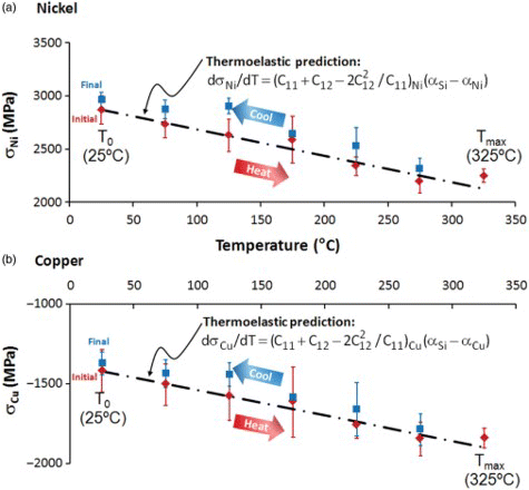
(a) and (b) shows and
, respectively, for the Cu-11 nm/Ni-11 nm sample. Ni layers are in tension (2.9 GPa) and the Cu layers are in compression (1.4 GPa) at room temperature since d0 is smaller for Ni vs. Cu. Although these in-plane stresses are large, they are ∼50% of the stresses for purely coherent interfaces. Also, the stresses in Cu and Ni are not equal and opposite due to the presence of the Cu seed layer and Si substrate. During heating, the metals expand more than the Si substrate since
and
. Therefore,
becomes less positive and
becomes more negative during heating. The dashed line in each plot shows the predicted slope
for each layer assuming they deform thermoelastically (i.e. no plasticity). The slope is obtained by differentiating Equation (4) to obtain
, where
from Equation (7). This approximation captures the experimental measurements to within an average of 4% error.
Figure 2. Average in-plane biaxial stress (a) σNi and (b) σCu vs. temperature for the Cu-11 nm/Ni-11 nm multilayer sample. The dashed lines and governing equations are predictions from Equation (4) assuming no inelastic deformation (i.e. thermoelastic only).
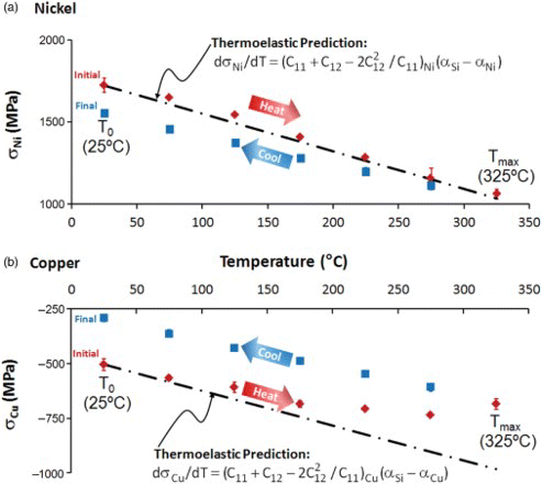
(a) and (b) shows and
, respectively, for the Cu-21 nm/Ni-21 nm sample. The initial stresses in both layers are smaller than those in the Cu-11 nm/Ni-11 nm film, indicating a less coherent system. As before, the stresses in the Cu and Ni layers are not equal and opposite. Noticeable deviations from thermoelastic behavior are apparent, implying
. In Ni, the deviation occurs only upon cooling. In Cu, the deviation occurs for heating above 200°C, as well as over most of the cooling range. After a thermal cycle,
is ∼10% lower and
is 40% lower. This may reflect dislocation-based plasticity, interdiffusion between layers,[Citation32,Citation33] or diffusion-mediated processes such as constrained diffusional creep observed in single-phase thin films.[Citation15,Citation34]
Figure 3. Average in-plane biaxial stress (a) σNi and (b) σCu vs. temperature for the Cu-21 nm/Ni-21 nm multilayer sample. The dashed lines and governing equations are predictions from Equation (4) assuming no inelastic deformation (i.e. thermoelastic only).
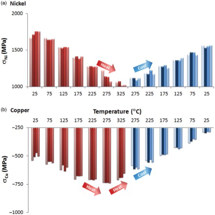
(a) and (b) shows and
, respectively, for the Cu-21 nm/Ni-21 nm sample, obtained from the four diffraction scans at each temperature. Each scan took ∼10 min with ∼2 min intervals between scans to reposition the goniometers. At each temperature, no evidence of uniform, time-dependent stress relaxation is observed from the first to fourth scans. The data for Ni at 275°C (heating) and Cu at 325°C do show monotonic decreases in stress of 12% and 7%, respectively, over these 40 min isothermal intervals, but the amount of decrease between consecutive scans is irregular. Overall, the aggregate of data supports time-independent plastic deformation rather than creep as the inelastic deformation.
Figure 4. Average in-plane biaxial stress (a) σNi and (b) σCu vs. temperature in the Cu-21 nm/Ni-21 nm multilayer sample, showing the results for four separate 10 min 2θ scans at each temperature. Overall, no systematic, time-dependent stress relaxation is evident.
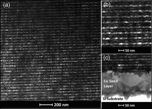
shows transmission electron microscope (TEM) micrographs of the Cu-21 nm/Ni-21 nm sample after the thermal cycle. The layer structure remains intact (a) and layer thickness is unchanged (b), suggesting that large-scale diffusion and morphological instability does not occur.[Citation35] The initially planar Si–Cu seed layer interface becomes nonplanar and nearby regions become polycrystalline (c), suggesting formation of copper silicides as in [Citation36]. Diffusion is aided by lack of an appropriate barrier layer. Nevertheless, this region is small compared with the overall film thickness and is not expected to account for the observed changes in or
. Other evidence of minimal interdiffusion is that the stress-free lattice parameter of Cu and Ni, calculated using the sin2Ψ-method and a procedure similar to Daniels et al.,[Citation32] changes by <0.2% after the thermal cycle. The lack of a systematic, time-dependent stress evolution at constant temperature is consistent with a time-independent inelastic mode of deformation such as confined layer slip, i.e. glide of single Orowan-type loops bounded by two interfaces.[Citation37,Citation38]
Figure 5. Bright-field TEM micrographs of the Cu-21 nm/Ni-21 nm after a single thermal cycle showing: (a, b) layer structure is maintained, with significant dislocation content at interfaces; (c) evidence that the Cu seed layer has reacted with the Si substrate but represents a small fraction of the overall film thickness.
shows (a) vs.
and (b)
vs.
for the Cu-21 nm/Ni-21 nm sample. During heating,
decreases with
, consistent with elastic unloading. During cooling,
increases ∼linearly by ∼500 MPa as plastic strain increases by
%. Gaps in the unloading vs. loading traces have been observed in conventional [Citation39,Citation40] and nanocrystalline metals [Citation41] following complete unloading and/or stress reversal under isothermal conditions. Here, the Ni layers are unloaded to only 60% of the initial stress. The elastic unloading indicates that dislocation loops in Ni (see inset, (a)) are unable to reverse direction during unloading, yet they readily move forward upon reloading. A possible explanation is that deformation in adjoining Cu layers has altered interfacial structure during unloading, thereby lowering the threshold for yield in Ni layers.
Figure 6. Average in-plane biaxial stress (a) σNi and (b) σCu vs. increment in plastic strain in the Cu-21 nm/Ni-21 nm multilayer sample. (a) Ni layers unload elastically during heating and reload plastically during cooling. Inset shows forward confined layer slip of dislocations in Ni. (b) Cu layers load plastically during heating, unload elastically during initial cooling, and then unload plastically during continued cooling. Inset (right) shows forward confined layer slip during heating and inset (left) shows reverse confined layer slip during continued cooling.
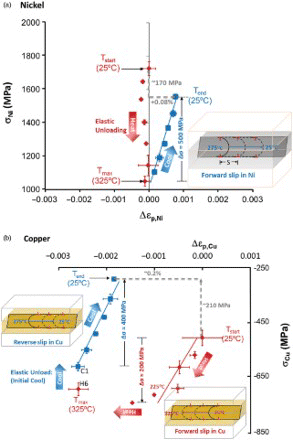
A peculiar feature is the large increase in stress MPa during the initial plastic strain increment
%. For comparison, 1 μm Ni thin films show
MPa,[Citation19] nanocrystalline Ni (29 nm average grain size) shows ∼240 MPa,[Citation42] and conventional grain size Ni shows ∼5 MPa.[Citation43] For consistency, these values are all measured during the initial 0.1% increment in plastic strain. The large value in the present experiments reflects that continued motion of existing dislocations or activation of new sources requires extraordinary increases in stress. Numerical and analytic calculations document strong interactions between threading and misfit dislocations [Citation44,Citation45] in multilayer thin films. Also, dislocation models of the work to increase interfacial misfit dislocation density [Citation46] in multilayer thin films support such large experimental values.
(b) shows MPa during heating.
plateaus at ∼740 MPa (compression). During initial unloading (cooling), Cu layers unload elastically by 80 MPa (Point H6 to C1 in (b)). Then reverse plastic deformation commences with continued unloading. Here,
MPa over the increment
%. This magnitude of stress change is comparable to those in loading/unloading of passivated Cu films (
nm) during plane-strain bulge tests.[Citation47] Although the changes in
and
are large in this initial plastic regime, corresponding changes in the macrostress on the Cu-21 nm/Ni-21 nm film, measured by micropillar compression, is only
MPa.[Citation48]
An unusual feature in (b) is the ∼linear recovery of plastic strain over a large (300 MPa) unloading range. Xiang and Vlassak [Citation47,Citation49] also observe plastic strain recovery in Cu layers (340–890 nm) using plane-strain bulge tests; Keller et al. [Citation23] report similar effects using substrate curvature tests. Both groups report large plastic strain recovery only if the Cu layer is passivated. Like the present work, the Xiang and Vlassak study reports plastic strain recovery prior to a reversal in the sign of applied stress. They attribute it to back stresses from dislocation pile-ups at the passivation/film interface. However, the nanoscale layers in the present study are more than an order of magnitude thinner, so that they are too small for significant pile-ups.[Citation1] Rather, the phenomena can stem from the driving force to remove dislocation line length at interfaces. This process is depicted in (b) insets and it has been observed in microscopy [Citation38,Citation50–52] and simulations.[Citation44,Citation53–56]
shows interfacial dislocation density (Equation (8)) vs. T for the Cu-21 nm/Ni-21 nm film. During heating,
increases ∼22% as Cu layers plastically compress and deposit dislocation content while Ni layers remain elastic (‘Heat’ inset, ). During cooling,
as Cu and Ni layers co-stretch by comparable plastic strain. Here, existing or new dislocation loops in Ni advance by forward slip while loops in Cu layers retract by reverse slip (‘Cool’ inset, ).
Figure 7. Evolution of net interfacial dislocation density ρinterface with temperature for the Cu-21 nm/Ni-21 nm film; during heating, ρinterface increases due to forward slip in Cu layers. During cooling, ρinterface ∼ constant due to ∼equal codeformation in Cu and Ni layers. Insets show forward and reverse confined layer slip in the presence of interfacial dislocations with spacing S and in-plane Burgers vector of magnitude be.
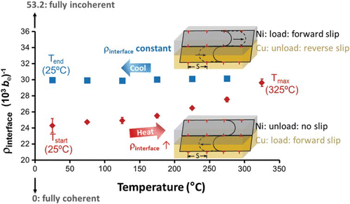
Carpenter et al. [Citation21] conclude that accumulation of interfacial dislocation content can serve to pin forward/reverse motion. It can also reduce the pinning dimension S for dislocations to bow-out from interfaces, thus impeding dislocation nucleation into adjoining layers. The average pinning strength in Cu can be estimated by comparing the biaxial stress for forward (heating) and reverse (cooling) modes ((b)):
Estimates of the pinning stress and average line energy are provided by applying Equation (9) to the difference in stress MPa at point H6 vs.
MPa at point C1 ((b)). The unloading is elastic, suggesting there is a difference in stress to move the same dislocation structure in the forward vs. reverse direction. An estimate
MPa is calculated using
from Equation (9). Similarly, an estimate
nJ/m is obtained using
from Equation (9), with
nm (averaged between Cu and Ni) and layer thickness h=21 nm. Thus, wCu is smaller than typical estimates of bulk line energy
nJ/m.[Citation57] This is consistent with interfaces that lower dislocation line energy, thereby trapping the dislocation.[Citation58]
The trends in pinning strength and line energy during heating and cooling are complicated by the interplay between temperature and interfacial dislocation density. During heating, interfacial dislocation density is estimated to increase by 22% (), corresponding to a decrease in average misfit dislocation spacing S from 41 to 34be. During the process, the Cu flow stress increases by 180 MPa (35%), despite potential softening induced by the temperature increase. During cooling, reverse flow occurs incrementally over a ∼300 MPa decrease in
, (b). Similar trends are observed in electrodeposited nanocrystalline Ni and are attributed to a wide grain-to-grain distribution in critical stress for slip.[Citation59] In the context of (b), the large increase in
upon heating may reflect that regions with favorable values of residual stress or relatively low threshold stress for slip are able to deform initially, thus redistributing stress to less favorable regions. Similarly, the unloading region with a decrease in
may reflect a wide distribution of internal stress and critical threshold for reverse motion.
The corresponding trends for Ni show that during heating/unloading, there is no reverse plasticity. This implies a large resistance to reverse plasticity (), which is estimated from Equation (9) to be
MPa. During cooling/reloading, it is remarkable that Ni readily undergoes forward yield, without any prior reverse yield. A hypothesis is that the increase in interfacial dislocation density (
during heating has introduced new sources that readily operate upon reloading. Thus, heating appears to work harden Cu layers but soften Ni layers.
Instrumented nanoindentation tests (MTS Nanoindenter XP with Continuous Stiffness Measurement) reveal room temperature hardness reductions of ∼2% (Cu-11 nm/Ni-11 nm) and ∼11% (Cu-21 nm/Ni-21 nm) caused by the heating/cooling cycle. shows the supporting pre- and post-thermal cycle values of hardness H and elastic modulus E, averaged between depths of 200–500 nm for 20 indents per sample. Corresponding values of biaxial stresses and
, average in-plane stress
on the multilayer film, and stress difference
values are provided. Based on finite element analyses by Chen et al., the pre and post changes in
are predicted to change H by 1% or less.[Citation60] This effect may account for the the minor (∼2%) H reduction in the Cu-11 nm/Ni-11 nm film, but not the larger (∼11%) H reduction in the Cu-21 nm/Ni-21 nm film. Other candidates for the large decrease include the 22% increase in
and the accompanying decrease in
. Prior work suggests that FCC/FCC samples derive strength from large
, which is maximized in the coherent interface limit.[Citation61] More recent work shows that sputtered Cu/Ni films with optimal combinations of
and
can give H values exceeding that for coherent films.[Citation21] In the present work, the heat/cool cycle appears to manipulate
and
in a deleterious way. More work is needed to elucidate the complicated dependence of H on stress state and interface structure, specifically the relative contributions of
,
and
on H.
Table 2. Hardness, elastic modulus and layer stresses pre- and post-thermal cycle.
To summarize, this work extends the use of heated in-plane X-ray diffraction to investigate constituent deformation behavior in multilayer thin films. The Cu-11 nm/Ni-11 nm multilayer with coherent interfaces displayed negligible plastic deformation even though GPa and
GPa were achieved during heating/cooling. The Cu-21 nm/Ni-21 nm case with semi-coherent interfaces did plastically deform, revealing peculiar features:
Enhanced reverse yielding in Cu layers, where reverse plastic flow occurs without changing the sign of average stress in Cu layers.
Large changes in flow stress,
MPa and
Estimate of line energy ∼0.8 nJ/m for dislocations deposited at [001 Cu/Ni interfaces during fully plastic flow. This estimate is ∼1/3 typical line energy estimates
Evidence that heating/cooling Cu-21 nm/Ni-21 nm multilayers reduces hardness by ∼11%. This H reduction is accompanied by a reduced internal (coherency) stress and increased net interfacial dislocation density.
The authors gratefully acknowledge discussions with Prof. William. D. Nix (Stanford), fabrication of the multilayer thin films by J. Kevin Baldwin (LANL), and TEM assistance from Matthew L. Bowers (OSU). This work was supported by the National Science Foundation (Division of Materials Research DMR-0907024, Diana Farkas, Program Officer). This research was conducted at the CNMS, which is sponsored at Oak Ridge National Laboratory by the Scientific User Facilities Division, Office of Basic Energy Sciences, US Department of Energy and by the CINT, a US Department of Energy, Office of Basic Energy Sciences user facility at Los Alamos National Laboratory (Contract DE-AC52-06NA25396) and Sandia National Laboratories (Contract DE-AC04-94AL85000).
REFERENCES
- Misra A, Hirth JP, Kung H. Single-dislocation-based strengthening mechanisms in nanoscale metallic multilayers. Philos Mag A. 2002 Nov;82:2935–2951. doi: 10.1080/01418610208239626
- Fu EG, Li N, Misra A, Hoagland RG, Wang H, Zhang X. Mechanical properties of sputtered Cu/V and Al/Nb multilayer films. Mater Sci Eng A. 2008 Oct;493(1–2):283–287. doi: 10.1016/j.msea.2007.07.101
- Li N, Yu KY, Lee J, Wang H, Zhang X. Size dependent strengthening mechanisms in sputtered Fe/W multilayers. J Appl Phys. 2010;107. Article no. 093503. doi: 10.1063/1.3400130
- Mara NA, Bhattacharyya D, Dickerson P, Hoagland RG, Misra A. Ultrahigh strength and ductility of Cu–Nb nanolayered composites. Mater Sci Forum. 2009 Nov;633–634:647–653. doi: 10.4028/www.scientific.net/MSF.633-634.647
- Zhang JY, Lei S, Liu Y, Niu JJ, Chen Y, Liu G, Zhang X, Sun J. Length scale-dependent deformation behavior of nanolayered Cu/Zr micropillars. Acta Mater. 2012 Feb;60(4):1610–1622. doi: 10.1016/j.actamat.2011.12.001
- Kim Y, Budiman AS, Baldwin JK, Mara NA, Misra A, Han SM. Microcompression study of Al–Nb nanoscale multilayers. J Mater Res. 2012;27(3):592–598. doi: 10.1557/jmr.2011.414
- Josell D, van Heerden D, Read D, Bonevich J, Shechtman D. Tensile testing low density multilayers: aluminum/titanium. J Mater Res. 1998;13(10):2902–2909. doi: 10.1557/JMR.1998.0397
- Huang H, Spaepen F. Tensile testing of free-standing Cu, Ag and Al thin films and Ag/Cu multilayers. Acta Mater. 2000 Jul;48(12):3261–3269. doi: 10.1016/S1359-6454(00)00128-2
- Mara NA, Bhattacharyya D, Hoagland RG, Misra A. Tensile behavior of 40 nm Cu/Nb nanoscale multilayers. Scripta Mater. 2008 May;58(10):874–877. doi: 10.1016/j.scriptamat.2008.01.005
- Budiman AS, Han S-M, Li N, Wei Q-M, Dickerson P, Tamura N, Kunz M, Misra A. Plasticity in the nanoscale Cu/Nb single-crystal multilayers as revealed by synchrotron laue X-ray microdiffraction. J Mater Res. 2012;27(3):599–611. doi: 10.1557/jmr.2011.421
- Aydıner CC, Brown DW, Mara NA, Almer J, Misra A. In situ X-ray investigation of freestanding nanoscale Cu–Nb multilayers under tensile load. Appl Phys Lett. 2009;94. Article no. 031906. doi: 10.1063/1.3074374
- Besser PR, Brennan S, Bravman JC. An X-ray method for direct determination of the strain state and strain relaxation in micron-scale passivated metallization lines during thermal cycling. J Mater Res. 1994;9(1):13–24. doi: 10.1557/JMR.1994.0013
- Doerner MF, Nix WD. Stresses and deformation processes in thin films on substrates. Crit Rev Solid State Mater Sci. 1988;14(3):225–268. doi: 10.1080/10408438808243734
- Keller R-M, Baker SP, Arzt E. Stress–temperature behavior of unpassivated thin copper films. Acta Mater. 1999;47(2):415–426. doi: 10.1016/S1359-6454(98)00387-5
- Balk TJ, Dehm G, Arzt E. Parallel glide: unexpected dislocation motion parallel to the substrate in ultrathin copper films. Acta Mater. 2003 Sep;51(15):4471–4485. doi: 10.1016/S1359-6454(03)00282-9
- Murakami M, Kuan TS. Thermal strain in lead thin films V: strain relaxation above room temperature. Thin Solid Films. 1980 Mar;66(3):381–394. doi: 10.1016/0040-6090(80)90391-0
- Kuru Y, Wohlschlögel M, Welzel U, Mittemeijer EJ. Coefficients of thermal expansion of thin metal films investigated by non-ambient X-ray diffraction stress analysis. Surf Coat Technol. 2008 Feb;202(11):2306–2309. doi: 10.1016/j.surfcoat.2007.08.002
- Eiper E, Keckes J, Martinschitz KJ, Zizak I, Cabié M, Dehm G. Size-independent stresses in Al thin films thermally strained down to −100°C. Acta Mater. 2007 Apr;55(6):1941–1946.
- Taylor AA, Oh SH, Dehm G. Microplasticity phenomena in thermomechanically strained nickel thin films. J Mater Sci. 2010 Apr;45(14):3874–3881. doi: 10.1007/s10853-010-4445-0
- Kraft O, Hommel M, Arzt E. X-ray diffraction as a tool to study the mechanical behaviour of thin films. Mater Sci Eng A. 2000 Sep;288(2):209–216. doi: 10.1016/S0921-5093(00)00876-5
- Carpenter JS, Misra A, Anderson PM. Achieving maximum hardness in semi-coherent multilayer thin films with unequal layer thickness. Acta Materialia. 2012 Apr;60(6–7):2625–2636. doi: 10.1016/j.actamat.2012.01.029
- Carpenter JS, Misra A, Uchic MD, Anderson PM. Strain rate sensitivity and activation volume of Cu/Ni metallic multilayer thin films measured via micropillar compression. Appl Phys Lett. 2012 Jul;101(5):051901–051901-4. doi: 10.1063/1.4739521
- Keller R-M, Baker SP, Arzt E. Quantitative analysis of strengthening mechanisms in thin Cu films: effects of film thickness, grain size, and passivation. J Mater Res. 1998;13(5):1307–1317. doi: 10.1557/JMR.1998.0186
- Birkholz M. Thin film analysis by X-ray scattering. Weinheim (Germany): Wiley-VCH publishing; 2005.
- Mitlin D, Misra A, Radmilovic V, Nastasi M, Hoagland R, Embury DJ, Hirth JP, Mitchell TE. Formation of misfit dislocations in nanoscale Ni–Cu bilayer films. Philos Mag. 2004;84(7):719–736. doi: 10.1080/14786430310001616072
- Cullity BD, Stock SR. Elements of X-ray diffraction. Upper Saddle River (NJ): Prentice Hall; 2001.
- Krishnan RS, Srinivasan R, Devanarayanan S. Thermal expansion of crystals. Oxford (England); New York: Pergamon Press; 1979.
- Watanabe H, Yamada N, Okaji M. Linear thermal expansion coefficient of silicon from 293 to 1000 K. Int J Thermophys. 2004 Jan;25(1):221–236. doi: 10.1023/B:IJOT.0000022336.83719.43
- Courtney TH. Mechanical behavior of materials. 2nd ed. Long Grove (IL): Waveland Pr Inc; 2005.
- Kraft O, Nix WD. Measurement of the lattice thermal expansion coefficients of thin metal films on substrates. J Appl Phys. 1998 Mar;83(6):3035–3038. doi: 10.1063/1.367118
- Fang W, Lo C-Y. On the thermal expansion coefficients of thin films. Sens Actuators A Phys. 2000 Sep;84(3): 310–314. doi: 10.1016/S0924-4247(00)00311-3
- Daniels BJ, Nix WD, Clemens BM. Effect of structure, stress, strain, and alloying on the hardness of Fe(001)/Pt(001) epitaxial multilayers. MRS Symp Proc. 1994;356:373–378. doi: 10.1557/PROC-356-373
- Villain P, Goudeau P, Badawi F, Ouyang G, Yang GW, Pélosin V. Physical origin of spontaneous interfacial alloying in immiscible W/Cu multilayers. J Mater Sci. 2007 Sep;42(17):7446–7450. doi: 10.1007/s10853-007-1605-y
- Weiss D, Gao H, Arzt E. Constrained diffusional creep in UHV-produced copper thin films. Acta Mater. 2001 Aug;49(13):2395–2403. doi: 10.1016/S1359-6454(01)00168-9
- Sperling EA, Banerjee R, Thompson GB, Fain JP, Anderson PM, Fraser HL. Processing and microstructural characterization of sputter-deposited Ni/Ni3Al multilayered thin films. J Mater Res. 2003;18(4): 979–987. doi: 10.1557/JMR.2003.0134
- Chang C-A. Formation of copper silicides from Cu(100)/Si(100) and Cu(111)/Si(111) structures. J Appl Phys. 1990 Jan;67(1):566–569. doi: 10.1063/1.345194
- Embury JD, Hirth JP. On dislocation storage and the mechanical response of fine scale microstructures. Acta Metall Et Mater. 1994;42(6):2051–2056. doi: 10.1016/0956-7151(94)90030-2
- Anderson PM, Foecke T, Hazzledine PM. Dislocation-based deformation mechanisms in metallic nanolaminates. MRS Bull. 1999;24:27–33.
- Cleveland R, Ghosh A. Inelastic effects on springback in metals. Int J Plast. 2002 Oct;18(5–6):769–785. doi: 10.1016/S0749-6419(01)00054-7
- Sun L, Wagoner RH. Complex unloading behavior: Nature of the deformation and its consistent constitutive representation. Int J Plast. 2011 Jul;27(7):1126–1144. doi: 10.1016/j.ijplas.2010.12.003
- Li L, Lee M-G, Anderson P. Critical strengths for slip events in nanocrystalline metals: predictions of quantized crystal plasticity simulations. Metall Mater Trans A. 2011;42(13):3875–3882. doi: 10.1007/s11661-010-0392-2
- Schuster BE, Wei Q, Zhang H, Ramesh KT. Microcompression of nanocrystalline nickel. Appl Phys Lett. 2006 Mar;88(10):103112–103112-3. doi: 10.1063/1.2183814
- Atlas of Stress–Strain Curves. Materials Park (OH): ASM International; 2002.
- Akasheh F, Zbib HM, Hirth JP, Hoagland RG, Misra A. Interactions between glide dislocations and parallel interfacial dislocations in nanoscale strained layers. J Appl Phys. 2007;102(3):034314. doi: 10.1063/1.2757082
- Fertig RS, Baker SP. Simulation of dislocations and strength in thin films: a review. Prog Mater Sci. 2009 Aug;54(6):874–908. doi: 10.1016/j.pmatsci.2009.03.004
- Kreidler ER, Anderson PM. Orowan-based deformation model for layered metallic materials. MRS Symp Proc. 1996;434:159–172. doi: 10.1557/PROC-434-159
- Xiang Y, Vlassak JJ. Bauschinger and size effects in thin-film plasticity. Acta Mater. 2006 Dec;54(20): 5449–5460. doi: 10.1016/j.actamat.2006.06.059
- Carpenter J. Estimates of interfacial properties in Cu/Ni multilayer thin films using hardness and internal stress data. Ann Arbor (MI): ProQuest, UMI Dissertations Publishing; 2010.
- Xiang Y, Vlassak JJ. Bauschinger effect in thin metal films. Scr Mater. 2005 Jul;53(2):177–182. doi: 10.1016/j.scriptamat.2005.03.048
- Kramer DE, Foecke T. Transmission electron microscopy observations of deformation and fracture in nanolaminated Cu–Ni thin films. Philos Mag A. 2002;82(17–18): 3375–3381. doi: 10.1080/01418610208240448
- Baker SP, Keller-Flaig R-M, Shu JB. Bauschinger effect and anomalous thermomechanical deformation induced by oxygen in passivated thin Cu films on substrates. Acta Mater. 2003;51(10):3019–3036. doi: 10.1016/S1359-6454(03)00113-7
- Mitlin D, Misra A, Mitchell TE, Hirth JP, Hoagland RG. Interface dislocation structures at the onset of coherency loss in nanoscale Ni–Cu bilayer films. Philos Mag. 2005;85(28):3379–3392. doi: 10.1080/14786430500145271
- Li Q, Anderson PM. Dislocation-based modeling of the mechanical behavior of epitaxial metallic multilayer thin films. Acta Mater. 2005 Feb;53(4):1121–1134. doi: 10.1016/j.actamat.2004.11.009
- Pant P, Schwarz KW, Baker SP. Dislocation interactions in thin FCC metal films. Acta Mater. 2003 Jun;51(11): 3243–3258. doi: 10.1016/S1359-6454(03)00156-3
- Fertig III RS, Baker SP. Dislocation dynamics simulations of dislocation interactions and stresses in thin films. Acta Mater. 2010 Sep;58(15):5206–5218. doi: 10.1016/j.actamat.2010.06.001
- Akasheh F, Zbib HM, Hirth JP, Hoagland RG, Misra A. Dislocation dynamics analysis of dislocation intersections in nanoscale metallic multilayered composites. J Appl Phys. 2007;101(8). Article no. 084314. doi: 10.1063/1.2721093
- Hirth JP, Lothe J. Theory of dislocations. Malabar (FL): Krieger Pub Co; 1992.
- Shen Y, Anderson PM. Transmission of a screw dislocation across a coherent, slipping interface. Acta Mater. 2006 Sep;54(15):3941–3951. doi: 10.1016/j.actamat.2006.04.026
- Li L, Anderson PM, Lee M-G, Bitzek E, Derlet P, Swygenhoven HV. The stress–strain response of nanocrystalline metals: a quantized crystal plasticity approach. Acta Mater. 2009 Feb;57(3):812–822. doi: 10.1016/j.actamat.2008.10.035
- Chen X, Yan J, Karlsson AM. On the determination of residual stress and mechanical properties by indentation. Mater Sci Eng A. 2006 Jan;416(1–2):139–149. doi: 10.1016/j.msea.2005.10.034
- Hoagland RG, Mitchell TE, Hirth JP, Kung H. On the strengthening effects of interfaces in multilayer FCC metallic composites. Philos Mag A. 2002;82(4):643.