
ABSTRACT
In this report, we have achieved a significant increase in the electrically active dopant fraction in Indium (In)-implanted Si0.35Ge0.65, by co-doping with the isovalent element Carbon (C). Electrical measurements have been correlated with X-ray absorption spectroscopy to determine the electrical properties and the In atom lattice location. With C + In co-doping, the solid solubility of In in Si0.35Ge0.65 was at least tripled from between 0.02 and 0.06 at% to between 0.2 and 0.6 at% as a result of C–In pair formation, which suppressed In metal precipitation. A dramatic improvement of electrical properties was thus attained in the co-doped samples.
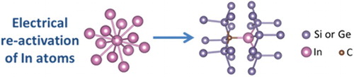
GRAPHICAL ABSTRACT
IMPACT STATEMENT
This work is the first to demonstrate that co-doping Carbon (C) with Indium (In) in SiGe is an effective strategy for obtaining high electrically active dopant fractions, which benefits advanced complementary metal-oxide semiconductor (CMOS) devices performance.
The low diffusion coefficient of In in Si makes it ideal for the realization of a steep doping profile to boost device scaling,[Citation1–3] while Ge has a superior carrier mobility [Citation4] and a shallow acceptor level for In (0.0112 eV above Ge valence band),[Citation5] which are advantageous to improve device electrical performance. Using Si1−xGex alloys and In as the dopant species has the potential to combine the positive aspects of both toward the application to CMOS devices.[Citation6] SiGe is a typical imperfect Pauling-type material, with compositional-dependent changes in the bond angle and length leading to unique effects on the impurity distribution.[Citation7] Yonenaga and Ayuzawa found that in Czochralski-grown SiGe, the segregation coefficients of In increased drastically compared to Ge and Si crystals.[Citation8] In our previous work,[Citation6] we found that the solid solubility of In in Si1−xGex decreased rapidly as a function of the substrate Si composition, from that of In in Ge (∼0.2 at%) [Citation6] toward that of In in Si (∼0.0036 at%).[Citation9] For instance, in the In-implanted Si0.35Ge0.65 samples, the formation of electrically inactive In metal precipitates was triggered at an In concentration as low as 0.06 at%, which affected the electrical activation of In significantly.[Citation6] Source and drain regions in advanced CMOS devices necessitate high dopant concentrations as well as high electrically active dopant fraction to reduce contact resistance and improve device performance.[Citation10] To this end, an above-equilibrium, metastable solid solubility limit for In in Si1−xGex is required.
Co-doping C with In is one of the most promising approaches to meet such a requirement. It has been reported that in both Si [Citation3,Citation11–13] and Ge,[Citation14–16] enhancement of In electrical activation was realized by C co-doping. Above-equilibrium solid solubility was attained in both substrates as a consequence of C–In pair formation that suppressed In precipitation. Intuitively, similar effects can be anticipated in Si1−xGex, despite earlier studies that found C did not bring beneficial impact to B activation in Si1−xGex.[Citation17–19] Furthermore, in Czochralski-grown Si doped with In, Inoue et al. found that co-doping of group-IV elements can uniquely affect the In concentration in the grown Si.[Citation20]
C co-doping has unique advantages over other co-doping or dopant reactivation strategies such as double accepter doping,[Citation1] flash annealing,[Citation21] pre-amorphization with solid phase epitaxy [Citation22,Citation23] and so on. As an isovalent element to Si and Ge, C has played important roles in Si1−xGex. By introducing C into Si1−xGex, dopant diffusion confinement can be achieved,[Citation24–26] and an extra degree of freedom can be added to the strain [Citation27–29] and bandgap engineering [Citation30–32] of Si1−xGex. The effect of C on the Si1−xGex bandgap expansion is crucial, since the narrow bandgap of high Ge composition Si1−xGex is a substantial issue that causes a high off-state leakage due to band-to-band tunneling.[Citation33] (The bandgap of Si and Ge are 1.12 and 0.66 eV, respectively, while that of diamond is 5.5 eV.) In fact, as C-doped Si1−xGex outperforms Si1−xGex in many areas, the Si1−x−yGexCy ternary semiconductor was proposed to replace Si1−xGex in advanced electronic device fabrication.[Citation34,Citation35] The material is now even more promising, given that this work shows C also has the capability of enhancing the solid solubility of In in Si1−xGex, which improves the In electrical activation.
In this report, Hall effect measurements demonstrate a significant increase of In electrically active fraction in Si0.35Ge0.65 in the presence of C. Correlating that with the structural characterization performed using X-ray absorption spectroscopy (XAS), such an electrical activation increase was found to be the result of In solid solubility enhancement in Si0.35Ge0.65 due to C co-doping. We examined a range of C and In concentrations (0.02–0.6 at%), the latter at device-appropriate levels, to establish the concentration-dependent effectiveness of this approach.
Undoped Si0.35Ge0.65 layers of thickness 2.5 µm, deposited on (100) Si substrates by molecular beam epitaxy, were implanted with C and In ions. We used a SiGe/Si heterostructure to enable the subsequent removal of the Si substrate for superior synchrotron-based measurements.[Citation36] The influence of misfit dislocations near the SiGe/Si interface (due to the lattice mismatch between SiGe and Si) was minimized by confining the implanted C and In depth distributions to <2 µm. Implantations were performed at 250°C to avoid amorphization and the surface normal was offset 7° from the incident ion direction to avoid channeling. C ions were first implanted, with three ion energies (450, 750 and 1,000 keV) and variable fluences (5.02 × 10¹⁴−2.15 × 10¹⁶ ions/cm2) to produce a uniform C depth distribution over about 0.75–1.75 µm, as calculated with TRIM-2008.[Citation37] In ions were then implanted with ion energies and fluences appropriate to yield overlapping C and In depth distributions, and at the same concentration as C in each sample (C: In = 1:1). The In implantation details are given in a previous report.[Citation6] The In concentrations (0.02–0.6 at%) were determined with Rutherford back scattering after annealing. A three-step annealing process in N2, at temperatures of 700°C, 550°C and 400°C for 0.5, 1 and 2 h, respectively, was used to initially activate the implanted In atoms and reduce lattice disorder (700°C) and then enhance the concentration of In-defect configuration by lowering the solid solubility limit (400°C). For the electrical characterization, samples were patterned into clover-leaf van der Pauw geometries of 1 cm radius for high-measurement accuracy [Citation38] by means of photolithography and wet etching. To achieve an Ohmic contact, four 0.75 mm diameter, 200 nm thick Al contacts were thermally evaporated on the corners of the sample surface. The Ohmic nature of the contacts was confirmed with I–V measurements. Fluorescence-mode extended X-ray absorption fine structure (EXAFS) measurements were performed at the XAS beamline of the Australian Synchrotron, with data analysis carried out using the IFFEFIT package [Citation39] and FEFF9 code.[Citation40] The input models to the EXAFS simulation were firstly geometrically optimized with complimentary density functional theory (DFT) calculations performed with the Vienna Ab initio Simulation Package code.[Citation41] Cross-sectional Transmission Electron Microscopy (TEM) measurements were performed with a Phillips CM300 operating at 300 kV. The direction of observation is close to the [110] direction from Si1−xGex parallel to the (001) plane from the surface. Samples were prepared with conventional methods: mechanical grinding to 80 µm, dimple grinding to 10–20 µm then final polishing using Ar ion milling with the sample maintained at liquid N2 temperature.
Figure compares the resistivity, carrier density and carrier mobility of In and C + In-implanted Si0.35Ge0.65 samples as a function of In concentration. All samples exhibited p-type conductivity. The EXAFS spectra of the In and C + In co-doped samples are compared in Figure , and results are summarized in Table .
Figure 1. (a) Resistivity, (b) carrier density and (c) carrier mobility as a function of In concentration. Squares and circles represent In-doped Si0.35Ge0.65 [6] and C + In co-doped Si0.35Ge0.65, respectively. In panel (b), un-bracketed and bracketed numbers are the electrically active fractions for In-doped Si0.35Ge0.65 [6] and C + In co-doped Si0.35Ge0.65, respectively.
![Figure 1. (a) Resistivity, (b) carrier density and (c) carrier mobility as a function of In concentration. Squares and circles represent In-doped Si0.35Ge0.65 [6] and C + In co-doped Si0.35Ge0.65, respectively. In panel (b), un-bracketed and bracketed numbers are the electrically active fractions for In-doped Si0.35Ge0.65 [6] and C + In co-doped Si0.35Ge0.65, respectively.](/cms/asset/2b02bb37-cb17-4451-b8e2-0e083187df21/tmrl_a_1169229_f0001_c.jpg)
Figure 2. The Fourier-transformed, k2-weighted EXAFS spectra as a function of radial distance for (a) the In-doped Si0.35Ge0.65 [6] and (b) C + In co-doped Si0.35Ge0.65 samples, respectively.
![Figure 2. The Fourier-transformed, k2-weighted EXAFS spectra as a function of radial distance for (a) the In-doped Si0.35Ge0.65 [6] and (b) C + In co-doped Si0.35Ge0.65 samples, respectively.](/cms/asset/2d4a0d23-4021-44db-9421-085c818f733a/tmrl_a_1169229_f0002_c.jpg)
Table 1. A summary of the quantified fractions (from Figure ) of In atoms in substitutional sites (S), metallic In (M), random lattice location (R) and substitutional sites pairing with C (C) of the In [6] and C + In-implanted Si0.35Ge0.65 samples.
At low In concentration (0.02 at%), co-doping leads to a minor increase and decrease of carrier density and Hall mobility, respectively, yielding a similar resistivity to the sample without C. The effect of C co-doping on the electrical properties was negligible at this concentration (0.02 at%). The analysis of the EXAFS spectra (Figure ) shows that all implanted In atoms occupied substitutional lattice sites (S sites) and were four-fold coordinated in both the singly doped and co-doped samples (Table ). Thus, with or without C present, no evidence of electrically inactive In metal precipitates (In atoms in M site) was apparent. This correlates well with the electrical measurements, where the vast majority of In atoms were electrically active in both the 0.02 at% In-doped and C + In co-doped samples.
As Figure demonstrates, the influence of co-doping was more significant at higher In concentrations. At 0.06 at%, the In activation ratio increased from 60.1% to 90.4% due to C co-doping, while the carrier mobility decreased as a result of increased lattice disorder and ionized impurity scattering.[Citation33] An obvious resistivity reduction was observed. This improvement of the electrical activation is a result of C-induced In solid solubility enhancement in Si0.35Ge0.65. The EXAFS fits (Figure (a)) shows that without C, ∼ 26% of the implanted In atoms in Si0.35Ge0.65 formed In metal precipitates at this concentration (0.06 at%, in Table ). However, with C present (0.06 at.% C + In), the In metal-related EXAFS scattering peaks (Figure (b)) are not visible. The fits of the spectra confirmed all implanted In are in S sites (as shown in Table ). Evidence of C–In pairing was not found in this sample, and the concentration of the C–In pairs is expected to be lower than the delectable limit of EXAFS.
The greatest effect of C + In co-doping was observed at an In concentration of 0.2 at%. According to the EXAFS analysis (Figure (a)) of the 0.2 at% In singly doped Ge sample, ∼67% of the In dopants in Si0.35Ge0.65 were in an In metal environment (M site), only ∼33% and ∼23% of the In atoms were in S site and electrically active (Table and Figure ), respectively. The suppression of In metal precipitate formation was achieved with C co-doping at this In concentration (0.2 at%). The corresponding EXAFS spectrum (Figure (b)) remains similar to that of substitutional, four-fold coordinated In with no evidence of metallic In. Fitting the EXAFS spectrum using In atoms in a substitutional site of SiGe lattice yielded a low-quality fit and non-physical DWFs. An improved fit was obtained using a DFT relaxed model of a C–In pair in a substitutional site of Si0.35Ge0.65. The bond lengths determined from this method agree well with those from the DFT model, implying that the model is a good match to the actual atomic structure of the sample.[Citation14,Citation33] The coordination number of C to In is a variable in our fitting (this approach is based on [Citation14]) and shows that one In atom was on average paired with 0.75 ± 0.13 C atoms. Thus, we expected that ∼75% of the implanted In atoms formed C–In pairs (in C site), and 25% remained in a S site without C bonding (Table ). A fit of the C + In-doped 0.2 at% sample with additional In metal fraction was also tested, but yielded no evidence of metallic In. Our TEM study of the samples further supported the EXAFS analysis. As shown in Figure (a), In metal precipitation was readily visible in the 0.2 at% In-implanted SiGe sample, while no In precipitation is apparent from the 0.2 at% C + In-implanted sample (Figure (b)). C–In pair formation was supported by our DFT calculations, with the calculated value for C–In binding energy in a substitutional site in Si0.35Ge0.65 of −0.35 eV. This effectively shows that C–In pairing is indeed energetically favorable in Si0.35Ge0.65. The reduction of In metal fraction due to C co-doping resulted in a dramatic increase of the 0.2 at% C + In sample dopant activation ratio (from 23.1% to 40.2%), along with a resistivity decrease from about 5–3.5 mΩ × cm as shown in Figure . The low amplitude of the 0.2 at% co-doped sample EXAFS spectrum implied (high Debye–Waller factors values were used in the fit) a high level of disorder in the In local environment. This is responsible for the relatively low In electrically active fraction (40.2%), given that In metal precipitation was not found in the sample. C–In pair formation as well as its similar effects on In solid solubility and electrical activation enhancement were observed in both C + In co-doped Si [Citation3,Citation11–13] and Ge,[Citation14–16] consistent with our results here with Si0.35Ge0.65.
Figure 3. Cross-sectional TEM images for (a) 0.2 at% In doped Si0.35Ge0.65 and (b) 0.2 at% C + In co-doped Si0.35Ge0.65.
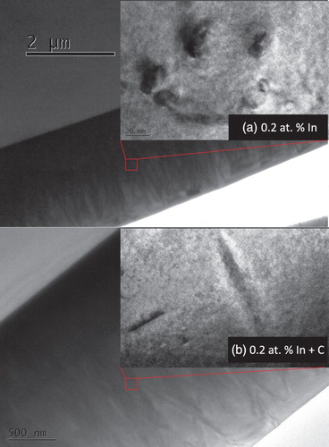
At the highest In concentration of 0.6 at%, In metal precipitation was found in both the In-implanted (Figure (a)) and C + In co-implanted (Figure (b)) samples. This indicated that even with the introduction of C, 0.6 at% was still beyond the solid solubility threshold of In in Si0.35Ge0.65. C co-doping enhanced the In solid solubility limit of Si0.35Ge0.65 from between 0.02 and 0.06 at% to between 0.2 and 0.6 at%, a (at least) three-fold increase was attained. At this concentration (0.6 at%), the EXAFS analysis shows that ∼81% and ∼67% (Table ) of the doped In atoms were on M sites of Si0.35Ge0.65 for the singly implanted and co-implanted samples, respectively. The lower metal fraction in the co-doped sample was also an indication of the enhanced solid solubility. Note that to achieve improved EXAFS fittings, a fitting component of In atoms in a random location (R site) with no contribution to the EXAFS spectra [Citation42] was introduced. As shown in Figure , the formation of electrically inactive In metal precipitates in the (0.6 at%) co-doped sample caused a low In active ratio (12.7%), only a minor improvement from the one without C (9.1%), along with a slightly lower resistivity and Hall mobility.
In conclusion, we have characterized the electrical and structural properties of C + In co-doped Si0.35Ge0.65, demonstrating this approach can yield a significant increase in carrier density relative to a conventional single dopant implantation protocol. An above-equilibrium solid solubility limit of In in Si0.35Ge0.65 was achieved with C–In pairing, which was at least three times greater than that without C. As a consequence, the formation of In precipitates was effectively suppressed and the carrier density was enhanced. Our experimental identification of the In atom lattice site and electrically active fraction demonstrates that co-doping with C is an effective strategy for obtaining the high electrically active dopant fractions required for advanced devices.
Acknowledgements
We acknowledge access to NCRIS and AMMRF infrastructure at the Australian National University including the Australian National Fabrication Facility, the Heavy Ion Accelerator Capability and the Center for Advanced Microscopy.
Disclosure statement
No potential conflict of interest was reported by the authors.
ORCID
Salvy P. Russo http://orcid.org/0000-0003-3589-3040
Additional information
Funding
References
- Yamauchi J, Aoki N. Deactivation mechanism of In atoms doped in a Si crystal and reactivation due to codoping with B and C. Phys Rev B. 2005;71:205205. doi: 10.1103/PhysRevB.71.205205
- Decoster S, de Vries B, Wahl U, Correia JG, Vantomme A. Lattice location study of implanted In in Ge. J Appl Phys. 2009;105:083522. doi: 10.1063/1.3110104
- d'Acapito F, Shimizu Y, Scalese S, Italia M, Alippi P, Grasso S. Experimental determination of the local geometry around In and In-C complexes in Si. Appl Phys Lett. 2006;88:212102. doi: 10.1063/1.2206703
- Hull R and Bean JC. Germanium silicon: physics and materials, semiconductors and semimetals. San Diego: Academic; 1999.
- Geballe TH and Morin FJ. Ionization energies of groups III and V elements in Germanium. Phys Rev. 1954;95:1085–1086. doi: 10.1103/PhysRev.95.1085
- Feng R, Kremer F, Sprouster DJ, et al. Structural and electrical properties of In-implanted Si1−xGex alloys. J Appl Phys. 2016;119:025709. doi: 10.1063/1.4940046
- Yonenaga I and Sakurai M. Bond lengths in Ge1−xSix crystalline alloys grown by the Czochralski method. Phys Rev B. 2001;64:113206. doi: 10.1103/PhysRevB.64.113206
- Yonenaga I and Ayuzawa T. Segregation coefficients of various dopants in SixGe1−x (0.93 < x < 0.96) single crystals. J Cryst Growth. 2006;297:14–19. doi: 10.1016/j.jcrysgro.2006.08.044
- Solmi S, Parisini A, Bersani M, et al. Investigation on indium diffusion in silicon. J Appl Phys. 2002;92:1361. doi: 10.1063/1.1492861
- Duffy R, Shayesteh M, Kazadojev I, Yu R. Germanium doping challenges. Paper presented at: 13th International Workshop on Junction Technology (IWJT); 2013 June 6–7; Kyoto, Japan.
- Boudinov H, de Souza JP, Saul CK. Enhanced electrical activation of indium coimplanted with carbon in a silicon substrate. J Appl Phys. 1999;86:5909–5911. doi: 10.1063/1.371611
- Scalese S, Italia M, La Magna A, et al. Diffusion and electrical activation of indium in silicon. J Appl Phys. 2003;93:9773. doi: 10.1063/1.1572547
- d’Acapito F, Shimizu Y, Scalese S, Italia M, Alippi P, Grasso S. The effect of thermal treatments on the local geometry around indium in In and In+C high dose implanted Si. Nucl Instr and Meth in Phys Res B. 2006;253:59–62. doi: 10.1016/j.nimb.2006.10.014
- Tessema G, Vianden R. Indium–carbon pairs in germanium. J Phys Condens Matter. 2003;15:5297–5306. doi: 10.1088/0953-8984/15/30/311
- Chroneos A. Effect of carbon on dopant–vacancy pair stability in germanium. Semicond Sci Technol. 2011;26:095017. doi: 10.1088/0268-1242/26/9/095017
- Feng R, Kremer F, Sprouster DJ, et al. Enhanced electrical activation in In-implanted Ge by C co-doping. Appl Phys Lett. 2015;107:212101. doi: 10.1063/1.4936331
- Osten HJ, Lippert G, Gaworzewski P, Sorge R. Impact of low carbon concentrations on the electrical properties of highly boron doped SiGe layers. Appl Phys Lett. 1997;71:1522–1524. doi: 10.1063/1.119955
- Noda T, Lee D, Shim H, Sakuraba M, Matsuura T, Murota J. Doping and electrical characteristics of in-situ heavily B-doped Si1−x−yGexCy films epitaxially grown using ultraclean LPCVD. Thin Solid Films. 2000;380:57–60. doi: 10.1016/S0040-6090(00)01469-3
- Noh J, Takehiro S, Sakuraba M, Murota J. Relationship between impurity (B or P) and carrier concentration in SiGe(C) epitaxial film produced by thermal treatment. Appl Surf Sci. 2004;224:77–81. doi: 10.1016/j.apsusc.2003.08.046
- Inouea K, Taishib T, Tokumotoa Y, et al. Czochralski growth of heavily indium-doped Si crystals and co-doping effects of group-IV elements. J Cryst Growth. 2014;393:45–48. doi: 10.1016/j.jcrysgro.2013.10.033
- Lanzerath F, Buca D, Trinkaus H, et al. Boron activation and diffusion in silicon and strained silicon-on-insulator by rapid thermal and flash lamp annealings. J Appl Phys. 2008;104:044908. doi: 10.1063/1.2968462
- Mirabella S, Impellizzeri G, Piro AM, Bruno E, Grimaldi MG. Activation and carrier mobility in high fluence B implanted germanium. Appl Phys Lett. 2008;92:251909. doi: 10.1063/1.2949088
- Chao Y-L, Prussin S, Woo JCS, Scholz R. Preamorphization implantation-assisted boron activation in bulk germanium and germanium-on-insulator. Appl Phys Lett. 2005;87:142102. doi: 10.1063/1.2076440
- Osten HJ. Effects of carbon on boron diffusion in SiGe: principles and impact on bipolar devices. J Vac Sci Technol B. 1998;16:1750–1753. doi: 10.1116/1.590048
- Rajendran K, Schoenmaker W. Modeling of complete suppression of boron out-diffusion in Si1−xGex by carbon incorporation. Solid-State Electron. 2001;45:229–233. doi: 10.1016/S0038-1101(01)00012-0
- Rizk S, Haddara YM, Sibaja-Hernandez A. Modeling the suppression of boron diffusion in Si/SiGe due to carbon incorporation. J Vac Sci Technol B. 2006;24:1365–1370. doi: 10.1116/1.2198858
- Eberl K, Iyer SS, Zollner S, Tsang JC, LeGoues FK. Growth and strain compensation effects in the ternary Si1−x−yGexCy alloy system. Appl Phys Lett. 1992;60:3033–3035. doi: 10.1063/1.106774
- Amour AST, Liu CW, Sturm JC, Lacroix Y, Thewalt MLW. Defect-free band-edge photoluminescence and band gap measurement of pseudomorphic Si1−x−yGexCy alloy layers on Si (100). Appl Phys Lett. 1995;67:3915–3917. doi: 10.1063/1.115316
- Mukerjee S, Venkataraman V. Ellipsometric investigation of strain reduction in Si1−x−yGexCy layers compared to Si1−xGex layers on silicon. Solid-State Electron. 2001;45:1875–1877. doi: 10.1016/S0038-1101(01)00226-X
- Soref RA. Optical band gap of the ternary semiconductor Si1−x−yGexCy. J Appl Phys. 1991;70:2470–2472. doi: 10.1063/1.349403
- Osten HJ. Band-gap changes and band offsets for ternary Si1−x−yGexCy alloys on Si(001). J Appl Phys. 1998;84:2716–2721. doi: 10.1063/1.368383
- Rezki M, Tadjer A, Abid H, Aourag H. Electronic structure of Si1−x−yCxGey. Mater Sci Eng B. 1998;55:157–161. doi: 10.1016/S0921-5107(98)00110-X
- Kuhn KJ, Murthy A, Kotlyar R, Kuhn M. Past, present and future: SiGe and CMOS transistor scaling. ECS Trans. 2010;33:3–17. doi: 10.1149/1.3487530
- Quinones EJ, John S, Ray SK, Banerjee SK. Design, fabrication, and analysis of SiGeC heterojunction PMOSFETs. IEEE Trans Electron Devices. 2000;47:1715–1725. doi: 10.1109/16.861582
- Schubert MF, Rana F. SiGeC/Si electrooptic modulators. J Lightwave Technol. 2007;25:866–874. doi: 10.1109/JLT.2006.890432
- Feng R, Kremer F, Sprouster DJ, et al. Structural and electrical properties of In-implanted Ge. J Appl Phys. 2015;118:165701. doi: 10.1063/1.4934200
- Ziegler JF and Manoyan JM. The stopping of ions in compounds. Nucl Instrum Methods Phys Res Sec B. 1998;35:215–228. doi: 10.1016/0168-583X(88)90273-X
- de Mey G. Field calculations in Hall samples. Solid-State Electron. 1973;16:955–957. doi: 10.1016/0038-1101(73)90105-6
- Newville M. IFEFFIT : interactive XAFS analysis and FEFF fitting. J Synchrotron Rad. 2001;8:322–324. doi: 10.1107/S0909049500016964
- Rehr JJ, Kas JJ, Vila FD, Prange MP, Jorissen K. Parameter-free calculations of X-ray spectra with FEFF9. Phys Chem Chem Phys. 2010;12:5503–5513. doi: 10.1039/b926434e
- Kresse G, Furthmüller J. Efficient iterative schemes for ab initio total-energy calculations using a plane-wave basis set. Phys Rev B. 1996;54:11169–11186. doi: 10.1103/PhysRevB.54.11169
- Decoster S, Johannessen B, Glover CJ, et al. Direct observation of substitutional Ga after ion implantation in Ge by means of extended x-ray absorption fine structure. Appl Phys Lett. 2012;101:261904. doi: 10.1063/1.4773185