
ABSTRACT
We report a novel method for synthesis and processing of pure and nitrogen-vacancy (NV)-doped nanodiamonds with sharp NV0 and NV− transitions at ambient temperatures and pressures in air. Carbon films are melted by nanosecond lasers in super undercooled state and quenched rapidly. We can form single-crystal nanodiamonds, microdiamonds, nanoneedles and microneedles, and large-area films. Substitutional nitrogen atoms and vacancies are incorporated into diamond during rapid liquid-phase growth, where dopant concentrations can far exceed thermodynamic solubility limits through solute trapping. These nanodiamonds can be placed deterministically and the transitions between NV− and NV0 can be controlled electrically and optically by laser illumination.
GRAPHICAL ABSTRACT
IMPACT STATEMENT
This research represents a fundamental breakthrough in controlled synthesis of nanodiamonds and doping of diamond with NV centers in nanostructures needed for quantum devices operating at room temperature.
Introduction
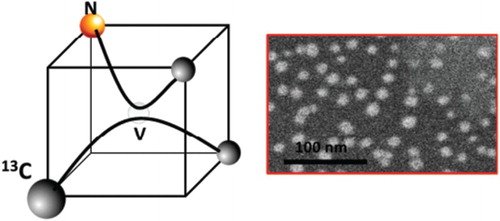
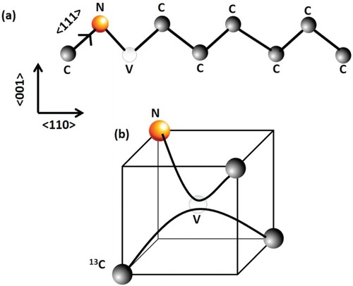
Pure and nitrogen-doped nanodiamonds are non-toxic, and have excellent electronic, magnetic, optical and mechanical properties with applications ranging from drug delivery and fluorescent biomarkers to single-photon sensors and quantum computing, nanoscale electronic and magnetic sensing, single-spin nuclear magnetic resonance, nanoscale thermometry and nanosensors [Citation1,Citation2]. The nitrogen-vacancy (NV) center in diamond is a point defect in diamond with C3v symmetry consisting of substitutional nitrogen and vacancy pair along <111> directions. Considering <110> chains, one of the links consists of a substitutional nitrogen and a lattice vacancy. (a) shows atomic structure of an NV defect in the <110> chains of diamond, and its structure in the diamond tetrahedron contained in the half (a/2, a/2, a/2) unit cell is shown in (b). These NV centers in diamond are quite stable, and are ideally suited for reliable and robust electronic, optical and magnetic nanoscale devices and systems operating at room temperature. The NV center is a deep-level defect, and it exists in neutral NV0 state and magnetically active NV− state with a trapped electron. The unique features of NV center are derived from spin triplet ground state and dependence of fluorescence on spin orientation. The EPR spectrum of a single NV center can be detected and shifts of EPR spectra are measured from perturbations in electric and magnetic fields, temperature, spatial orientation, strain and pressure. The magnetically active NV− defects are characterized by optical zero phonon line (ZPL) at 1.945 eV (637 nm), whereas NV0 has ZPL at 2.156 eV (575 nm). Associated vibronic bands extend ZPLs to lower and higher energy absorption and emission.
Figure 1. (a) Atomic structure of substitutional nitrogen and vacancy (NV) defect in <110> chain of diamond; and (b) NV defect in a diamond tetrahedron contained in (a/2,a/2,a/2) diamond unit cell, where one of the carbon can be replaced by magnetic isotope 13C.
The magnetically active NV− is also characterized by zero-field magnetic resonance at ∼2.88 GHz, which occurs between ms = 0 and ms = ± 1 spins with a g-factor of 2.0028 associated with 3A2 ground state. The optically detected magnetic resonance of NV− at ∼1.42 GHz is attributed to 3E ground state with g-factor of 2.01. Since NV− is magnetically active, its luminescence can be controlled by the magnetic field for various applications including single-photon sensors, nanoscale electronic and magnetic sensing, single-spin nuclear magnetic resonance, nanoscale thermometry, fluorescent biomarkers, quantum computing and nanosensors [Citation3].
The above applications require precisely controlled synthesis of pure and NV-doped diamonds, where NV defects can be located individually in various diamond structures such as nanodiamonds (4–10 nm), nanoneedles, microneedles and thin films. Current methods of introducing NV defects in diamond have many problems and challenges. The chemical vapor deposition (CVD)-based techniques produce large-grain polycrystalline films, and nanodiamonds produced by CVD [Citation4] have often embedded into amorphous carbon from which extraction of individual nanodiamond is quite cumbersome and expensive. Since nitrogen doping in CVD is controlled by thermodynamic solubility limit, the number density of NV centers per unit volume is quite limited. Second technique involves nitrogen ion implantation [Citation5]. The nitrogen ion implantation doping produces high concentration of Frenkel (vacancy-interstitial pairs) defects. For example, a single 50 KeV will produce roughly 100 Frenkel pairs [Citation6]. Annealing of these defects and putting nitrogen into substitutional sites represent many challenging problems, including high-thermal budgets. Third technique involves high-energy TNT detonation [Citation7]. The formation of nanodiamond by detonation (DND) are often aggregated and contaminated with detonation impurities, where purification and size control of DNDs are very problematic. The DNDs also have sp2 layer on the surface which must be removed to realize the optical properties of NV centers. Fourth technique is based upon laser ablation of carbon in water or liquid hydrocarbons with a limited yield [Citation8]. Fifth technique is based upon milling of bulk diamond produced by high-pressure and high-temperature method. Since the milling technique in diamond primarily involves fracturing process, the nanodiamonds produced by this method have uncontrolled shapes with drastically reduced nitrogen content [Citation9]. Since the bulk diamond before milling has only equilibrium concentration, further reduction from this value renders this technique quite ineffective and undesirable. More recently, another approach for the formation of nanodiamond from SiC has been reported at temperatures ∼1000°C under flowing hydrogen and chlorine gases at ambient pressures [Citation10]. However, the controlled introduction of nitrogen centers exceeding thermodynamic solubility limits in all of these nanostructures is still quite challenging.
In this paper, we report a direct conversion of pure and N-doped carbon into pure and N-doped diamond, where diamond is in the form of single-crystal nanodiamonds, nanoneedles, microneedles and thin films. Earlier work focused on the discovery of Q-carbon, Q-BN and direct conversion of carbon into diamond and h-BN into c-BN [Citation11–14]. Nanodiamonds are formed by homogeneous or heterogeneous nucleation from the undercooled melt, where the size is dictated by the melt lifetime. Nanoneedles and microneedles are formed as a result of interfacial instability of the crystallizing interface, which is controlled by laser and substrate variables, particularly thermal conductivity of the substrate. On the other hand, single-crystal film structures are created when substrate can act as a template for epitaxial growth. These nanodiamonds can be arranged periodically in a self-organized fashion, which is needed for quantum devices. The special emphasis is on N-doped (NV diamond) nanostructures with concentrations exceeding solubility limits, while comparing with our earlier results on undoped diamond nanostructures [Citation12–14]. Since diamond growth occurs from a liquid phase under ultrarapid quenching and solidification with velocity of the order of 5 m s−1, it is possible to trap NV defects beyond thermodynamic limits. A single NV defect in 5 nm or lower size diamond will require a higher concentration of nitrogen than its thermodynamic solubility limit of 2.0 × 1018 cm−3 [Citation15], which can be achieved by rapid quenching from the liquid, utilizing the phenomenon of solute trapping. The transitions between NV− and NV0 can be introduced electrically and optically by laser illumination. Using this method, we have achieved controlled doping of diamond with NV centers in a variety of nanostructures needed for many novel quantum nanotechnologies in physical and biological sciences, including single-photon sensors, quantum computing, nanoscale electronic and magnetic sensing, single-spin nuclear magnetic resonance, nanoscale thermometry, fluorescent biomarkers and nanosensors.
Experimental
In this method, carbon thin films are deposited on a substrate such as sapphire, glass and polymer to a desired thickness, where layer thickness ranges from 5 to 500 nm. These films are doped with nitrogen by two methods: (1) by adjusting the nitrogen partial pressure (5.0 × 10⁻³, 5.0 × 10⁻², 5.0 × 10⁻¹ Torr); and (2) by bombarding simultaneously with (0.5–1.0 KeV) during carbon thin film deposition. The nitrogen concentration is adjusted by controlling the nitrogen partial pressure and by measuring the nitrogen ion flux. Subsequently, these films are irradiated with high-power nanosecond laser pulses with energy density 0.5–1.0 J cm−2, pulse duration 20–40 ns and laser wavelength of 193 nm for ArF Excimer laser. The carbon film is melted in the highly super undercooled state and quenched within 200–250 ns. By controlling the quenching from the liquid, we can nucleate diamonds in the form of nanodiamonds (2–8 nm), microdiamonds (100–1000 nm), nanoneedles and microneedles up to 3000 nm long, and large-area thin films. By providing single-crystal substrate template, we are able to grow epitaxial single-crystal nanodiamonds, microdiamonds, nanoneedles and microneedles and large-area thin films. The characterization of diamond phase was carried by using electron backscatter diffraction (EBSD), Raman spectroscopy (532 nm source) and photoluminescence (PL) with 325 nm source. Detailed atomic structure and bonding characterization of various diamond structures using transmission electron microscopy/scanning transmission electron microscopy and electron energy loss spectroscopy have been already reported [Citation12–14]. Alfa300 R superior confocal Raman spectroscope with a lateral resolution less than 200 nm was employed to characterize the Raman active vibrational modes. Crystalline Si was used to calibrate the Raman spectra, which has its characteristic Raman peak at 520.6 cm−1. High-resolution SEM with sub nanometer resolution was carried out using FEI Verios 460L SEM to characterize the as-deposited and the laser irradiated films. EBSD HKLNordlys detector with less than 10 nm lateral resolution was used to map out Kikuchi diffraction pattern in FEI Quanta 3D FEG instrument in as-deposited and laser annealed thin films. The nitrogen is incorporated into diamond during rapid liquid-phase growth, where dopant concentrations can exceed far beyond the thermodynamic solubility limits. The number density of NV defects can be controlled by the nitrogen concentrations in the as-deposited films. A single NV defect in 5 nm diamond will require solubility limit of 1.5 × 1019 cm−3 (in excess of thermodynamic solubility limit of 2.0 × 1018 cm−3), which can be achieved by rapid quenching from the liquid, utilizing the phenomenon of solute trapping. Using this method, we have achieved controlled doping of diamond with NV centers in a variety of nanostructures.
Results and discussion
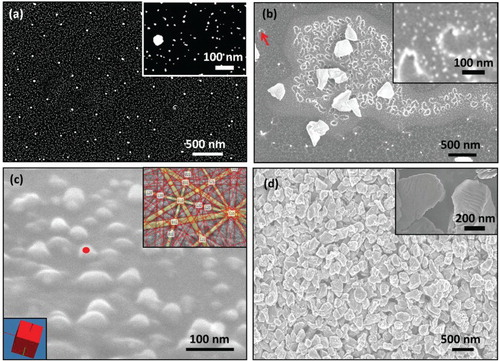
(a) shows the formation of undoped nanodiamonds after a single laser pulse, where the average size varied from 2 to 8 nm. These nanodiamonds nucleate from the highly undercooled carbon melt via homogeneous nucleation, and their size can be controlled by growth times during the quenching cycle. The larger sizes are formed as a result of heterogeneous nucleation, where sapphire acts as a template for diamond growth (heterogeneous nucleation). It is interesting to note that nanodiamonds are faceted down to this size range, as shown in the inset. During the initial stages or incipient carbon melting, the melting occurs in the form of rings, creating a ring of nanodiamonds, as shown in (b). This figure also shows the formation of Q-carbon and nucleation of nanodiamonds from Q-carbon. The larger diamond microcrystallites grow from the melt with increasing growth time. The nanodiamond growth around the super undercooled ring often has one larger nanodiamond, which is formed when two nucleation fronts around the ring collide, as shown in the inset at a higher magnification. The larger microdiamonds are formed, when sapphire substrate provides a template for epitaxial growth from super undercooled liquid. (c) shows the initial stages of the formation of self-organized nanodiamonds. The inset EBSD (from the red dot) confirms the diamond crystal structure, showing the characteristic Kikuchi diffraction pattern for diamond. The formation of string-like structure in a supercooled liquid has been explained as a result of spatial heterogeneity and dynamic facilitation in the regions having high atomic mobility, corresponding to high diffusivity in liquid of the order of 10−4 cm2 s−1. It is envisaged that coherent motion of carbon atoms within micro strings may facilitate the creation of neighboring excitations leading to the formation of observed ring structure of liquid carbon from which nanodiamonds are formed. Molecular dynamics simulations have shown string-like cooperative motion at temperatures well above the glass transition temperature. The mean length of the string increases upon cooling with nearly exponential distribution with temperature [Citation16,Citation17]. At a higher energy density, a full conversion of carbon into diamond microcrystallites is shown in (d). The inset at a higher magnification shows the details of faceting and twinning in microcrystals. It has been argued that twinning in diamond can lead to improvements in catalytic and mechanical properties. Here, we can vary the twin content by controlling the quenching rates from the melt, as shown by the formation of twins in the inset. The texture and orientation of these microcrystallites can be controlled by providing appropriate epitaxial template during growth from the liquid phase. In the present case, <111> oriented cubic diamond microcrystallites grow on (0001) sapphire, which are rotated with respect to each other by 30 degrees. The growth of three-fold cubic <111> diamond on hexagonal (0001) sapphire leads to twinning as result of two islands growing in a mirror symmetry [Citation14].
Figure 2. High-resolution SEM micrographs of nanodiamonds from pure undoped samples: (a) nanodiamonds with inset at a higher magnification; (b) mechanism of nanodiamond formation from Q-Carbon; (c) formation of nanodiamonds during initial stages and EBSD pattern (from red dot), showing characteristic diamond Kikuchi pattern; and (d) microdiamonds covering the entire area with inset showing twins whose density is controlled by quenching rates.
The nitrogen was introduced by two methods: (1) increasing the partial pressure of nitrogen during deposition; and (2) bombarding the carbon film with low-energy (0.5–1.0 KeV) ions. The
ions break into atomic nitrogen atoms upon impact, which are buried inside the film. The nitrogen concentration is controlled by the
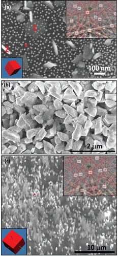
ion current. After laser annealing of the as-deposited nitrogen-doped carbon layers, we observe the formation of nanocrystals with an average size of 4–8 nm, as shown in the high-resolution SEM micrograph in (a). The figure also shows the formation of diamond platelets, some of which grow flat (as shown by 1) and others grow normal to the substrate (as shown by 2). The nanocrystals are faceted, which is similar to pure diamond nanocrystals. The characteristic diamond EBSD or Kikuchi pattern from a nanodiamond near the red dot is shown in the inset, confirming the structure of the diamond phase and orientation. Assuming one NVcomplex (NV center) in 4 nm diamond, the concentrations of N and V (3.0 × 1019 cm−3 each) exceed thermodynamic limit of 2.0 × 1018 cm−3 for nitrogen. Taking experimental value for the formation energy of a neutral vacancy in diamond to be 3.0 eV, the concentration is estimated to be ∼3.6 × 1019 cm−3 at 4000 K. Thus, NV centers with concentrations exceeding the solubility limits can be formed under quenching from the liquid through solute trapping phenomenon [Citation18]. The formation of two types of platelet crystals is clearly shown in (a). The faint contrast from flat diamond microcrystals is observed because these are formed near the sapphire interface and are buried under the carbon. The results on the formation of microcrystals of N-doped diamond are shown in (b). These microcrystals are formed with (0001) sapphire providing a template for epitaxial growth by domain matching epitaxy. The epitaxial relations of <111> diamond on (0001) sapphire are as follows: in-plane 19 (2d110) planes of diamond match with 20 (2d110) planes of sapphire [Citation19]. The formation of N-doped nanoneedles and microneedles is displayed in (c). From EBSD patterns, these nanoneedles and microneedles are single-crystals with sizes up to 2–3 microns. Under the liquid-phase growth, this will require crystal growth velocities of the order of 5 m s−1, which have been established in silicon under highly undercooled state during nanosecond laser annealing [Citation19].
Figure 3. High-resolution SEM micrographs of nanodiamonds and microdiamonds from N-doped samples: (a) nanodiamonds with inset diamond EBSD Kikuchi pattern and orientation (from red dot), it also shows flat nanodiamond nanoplates (indicated as 1) and perpendicular nanoplates of diamond (indicated as 2); (b) microdiamonds from N-doped samples containing twins; and (c) nanoneedles and microneedles from N-doped sample with inset characteristic diamond pattern and orientation from the spot indicated.
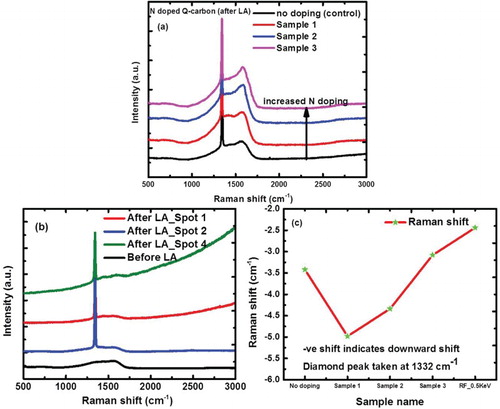
The Raman spectra from as-deposited carbon films as function of increasing nitrogen content (increasing partial pressure) are shown in (a). The partial pressure of nitrogen varied from 5.0 × 10⁻³ (for sample #1) to 5.0 × 10⁻² (for sample #2) to 5.0 × 10⁻¹ Torr (for sample #3). These Raman spectra contain D-peak at 1350 cm−1 and G-peak at 1550 cm−1. The nitrogen incorporation is signified by: (1) increasing the intensity ratio of I(D)/I(G); and (2) shift in the G-peak to higher wavenumber 1565 cm−1 The control sample with no-doping shows the lowest D-peak. After laser annealing, the Raman spectra from implanted sample is shown in (b). It shows a sharp diamond peak which is downshifted from 1332 cm−1 because of decreasing crystallite size. Considering phonon dispersion relations, the downshift for nanocrystalline diamond is expected, as the Raman active phonon is at the maximum frequency. The Raman spectra from nitrogen pressure-doped samples showed Raman peak around 1327 cm−1, which is downshifted from 1332 cm−1, but also contained residual signature of G-peak around 1560 cm−1. The results of Raman downshift for different N-doped samples, varying from 3 to 5 cm−1, are shown in (c). It should be mentioned that there is an upshift due to stresses, which is combined with downshift due to size. The Raman shift in diamond (Δω) is related to Δω (in cm−1) = 2.2 ± 0.10 cm−1 GPa−1 along the [111] direction, Δω (in cm−1) = 0.73 ± 0.20 cm−1 GPa−1 along the [100] direction and Δω (in cm−1) = 3.2 ± 0.23 cm−1 GPa−1 for the hydrostatic component [Citation17]. The biaxial stress in thin films can be described as a combination of two-thirds hydrostatic and one-third uniaxial stress. The biaxial stress can be estimated using σ = 2µ ((1 + >ν)/(1 − ν)). Δε, where µ is shear modulus, ν is Poisson’s ratio and Δε is the in-plain strain [Citation20].
Figure 4. Raman spectra from N-doped samples: (a) different N-doping by varying nitrogen pressure after laser treatment, including undoped control sample; (b) different N-doping by changing the ion flux after laser treatment, including the control (before laser annealing) sample; and (c) change in Raman shift, down shift due to size (nanorange) and upshift as a result of quenched-in stress.
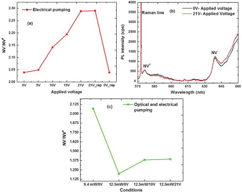
The PL spectra from these nanocrystal magnetically active NV− defects are characterized by optical ZPL at 1.945 eV (637 nm), whereas NV0 has ZPL at 2.156 eV (575 nm). shows that magnetically active NV− defects are characterized by optical ZPL at 1.945 eV (637 nm), whereas NV0 has ZPL at 2.156 eV (575 nm). These defects also exhibit associated vibronic bands, extending ZPLs to lower and higher energy absorption and emission. It is interesting to note that the characteristic NV− defect ZPL line from 5-nm diamond sample is indicative of the fact that these defects are contained in the individual nanodiamonds, which can be used for variety of biomedical and nanosensor applications. By using 532-nm PL source, it is possible to image in situ NV0 (575 nm) and NV− (637 nm) defects and their transitions from individual nanodiamonds directly, as, shown in the inset of . The sharpness of PL peaks is indicative of absence of other defects in nanodiamonds. Electrical and optical manipulation is essential for quantum device applications. Here, we show that transitions between NV− and NV0 can be introduced electrically and optically by laser illumination. (a) shows increase in NV−/NV0 with increasing applied voltage (current) up to a certain value and then saturates. This ratio is reduced to the initial value, when the applied voltage is reduced to zero. This is consistent with the equilibrium trapping and detrapping of carriers, as we can derive NV−/NV0 = (Kn/p)0.5, where K is the ratio of reaction constants and n and p are electron and hole concentration, respectively [Citation6]. The PL intensity measurements ((b)) show this enhancement in NV−/NV0 upon the application of voltage. (c) shows a reduction in NV−/NV0 upon laser illumination, which is consistent with generation and trapping of holes. The NV−/NV0 ratio decreases from 1 to 2 ((c)) as the laser power is increased from 9.4 to 12.5 mW without applying any voltage. When the voltage is applied at 12.5 mW, NV−/NV0 ratio increases with applied voltage from 10 (3) to 21 V (4). The increase from 3 to 4 is consistent with electrical pumping shown in (a).
Figure 5. PL spectrum containing ZPL from NV− (637 nm) and NV0 (575 nm) defects. The inset (100× magnification) shows transitions from individual nanodiamonds when the sample is irradiated with 532 nm PL source.
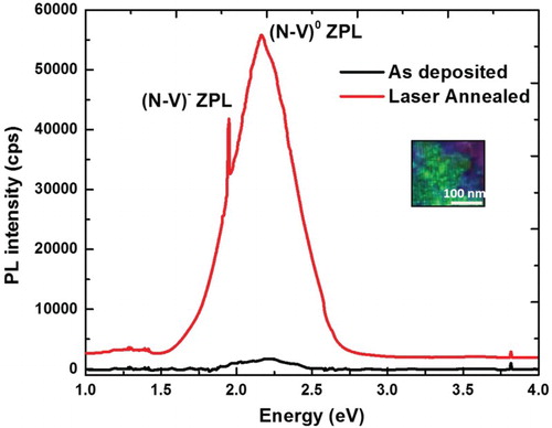
Figure 6. (a) Electrical pumping of NV centers using 14 mW laser power (532 nm excitation wavelength); (b) PL spectra of NV diamond in 0–21 V external electric field; and (c) optical and electrical pumping of NV centers using 532 nm laser.
Thus, electrical and optical manipulations can be used for deterministic charge-state control of NV− and NV0 centers, which is essential for quantum devices. Recently, it has been shown that NV− to NV0 transition can be induced by hole injection from p-type layers, enabling fast and deterministic charge control of a single NV center for a variety discrete quantum device applications [Citation21]. It should be mentioned that one of the carbon atoms in the diamond tetrahedron can be replaced by magnetic 13C in (b) to enhance entanglement among spins in diamond. Robust entanglement of several qubits at room temperature is critical for reliable quantum computing technology. It has been proposed that individual nuclear spins at 13C (magnetic isotope of carbon) can be controlled by their hyperfine coupling to a single electron of the NV center in diamond. In this system, quantum correlations are of high quality and persist over a millisecond at room temperature, which is adequate for advanced quantum operations. Using this approach, the generation and retrieval of entanglement among several qubits can be achieved for next-generation of quantum computing [Citation22].
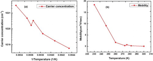
(a) provides the preliminary results on carrier concentration in N-doped diamond as a function of (1/T). The carrier concentration was found to vary from 2.0 × 10¹⁸ to 5.0 × 1021 cm−3. These high concentrations are the consequence of dopant trapping during rapid quenching. In the case of silicon, the dopant concentrations exceeding 400 times the solubility limits have been achieved as a result rapid solidification from the liquid phase.[Citation18] The phenomenon of formation of supersaturated silicon semiconductor alloys was modeled by solute trapping concepts which we expect to be applicable in the diamond case as well. The carrier mobility as a function of temperature for a sample with carrier concentration of 2.0 × 1019 cm−3 is shown in (b). This corresponds to conductivity of ∼25 Ω/cm at 250 K, which is quite reasonable. A fit to n = exp(−ΔE/kBT) suggest ΔE ∼0.53 eV.
Figure 7. (a) Carrier concentration plotted as 1/T; and (b) Hall mobility as a function of T.
Conclusions
In summary, we have created pure and N-doped diamond nanostructures in the form of nanodiamonds, microdiamonds, nanoneedles, microneedles, and large-area single-crystal thin films in a controlled way. This is achieved by rapid melting of carbon in a super undercooled state and quenching to convert carbon into diamond at ambient temperatures and pressures in air. The dopants such as nitrogen can be incorporated into diamond far in excess of solubility limit via solute trapping phenomena. The vacancy concentration corresponding to quenching temperature can be trapped with nitrogen to create NV centers in nanodiamonds and other structures exceeding the solubility limit. The NV− and NV0 defects have been characterized by PL using 325 nm wavelength, and NV− to NV0 transitions are controlled electrically by passing current and by laser irradiation with 532 nm photons. Controlled synthesis and processing of NV nanodiamonds and other structures opens next-generation of applications ranging from drug delivery and fluorescent biomarkers to single-photon sensors and quantum computing, nanoscale electronic and magnetic sensing, single-spin nuclear magnetic resonance, nanoscale thermometry and nanosensors. It has been speculated that pure and N-doped diamond nanostructures may exceed manufacturing volumes of fullerenes and other carbon nanomaterials.
Acknowledgements
We are also very pleased to acknowledge technical help and useful discussions with John Prater, Roger Narayan, and Ki-Wook Kim.
Disclosure statement
No potential conflict of interest was reported by the authors.
Additional information
Funding
References
- Doherty MW, Manson NB, Delaney P, et al. The nitrogen-vacancy colour centre in diamond. Phys Rep. 2013;528:1–45. doi: 10.1016/j.physrep.2013.02.001
- Schirhagl R, Chang K, Loretz M, et al. Nitrogen-vacancy centers in diamond: nanoscale sensors for physics and biology. Annu Rev Phys Chem. 2014;65: 83–105. doi: 10.1146/annurev-physchem-040513-103659
- Tisler J, Balasubramanian G, Naydenov B, et al. Fluorescence and spin properties of defects in single digit nanodiamonds. ACS Nano. 2009;3:1959–1965. doi: 10.1021/nn9003617
- Angus JC, Hayman CC. Low-pressure, metastable growth of diamond and ‘diamondlike’ phases. Science. 1988;241:913–921. doi: 10.1126/science.241.4868.913
- Pezzagna S, Naydenov B, Jelezko F, et al. Creation efficiency of nitrogen-vacancy centres in diamond. New J Phys. 2010;12:065017–065019. doi: 10.1088/1367-2630/12/6/065017
- Narayan J, Bhaumik A. N- and p-type doping diamond and c-BN beyond solubility limits, (to be published, US Patents Pending).
- Mochalin VN, Shenderova O, Ho D, et al. The properties and applications of nanodiamonds. Nat Nanotechnol. 2011;7:11–23. doi: 10.1038/nnano.2011.209
- Singh J, Vellaikal M, Narayan J. Laser-enhanced synthesis and processing of diamond films from liquid hydrocarbons. J Appl Phys. 1993;73:4351–4353. doi: 10.1063/1.352819
- Morita Y, Takimoto T, Yamanaka H, et al. A facile and scalable process for size-controllable separation of nanodiamond particles as small as 4 nm. Small. 2008;4:2154–2157. doi: 10.1002/smll.200800944
- Gogotsi Y, Welz S, Ersoy DA, et al. Conversion of silicon carbide to crystalline diamond-structured carbon at ambient pressure. Nature. 2001;411:283–287. doi: 10.1038/35077031
- Narayan J, Godbole VP, White CW. Laser method for synthesis and processing of continuous diamond films on nanodiamond substrates. Science. 1991;252:416–418. doi: 10.1126/science.252.5004.416
- Narayan J, Bhaumik A. Research update: direct conversion of amorphous carbon into diamond at ambient pressures and temperatures in air. APL Mater. 2015;3:100702–100704 , and two US Patents pending (62/245,108 (2015); 62/202,202 (2015); 62/331,217 (2016)). doi: 10.1063/1.4932622
- Narayan J, Bhaumik A. Research update: direct conversion of h-BN into pure c-BN at ambient temperatures and pressures in air. APL Mater. 2016;4:020701–020703. doi: 10.1063/1.4941095
- Narayan J, Bhaumik A. Novel phase of carbon, ferromagnetism, and conversion into diamond. J Appl Phys. 2015;118:215303–215305. doi: 10.1063/1.4936595
- Khomich AA, Kudryavtsev OS, Bolshakov AP, et al. Use of optical spectroscopy methods to determine the solubility limit for nitrogen in diamond single crystals synthesized by chemical vapor deposition. J Appl Spectrosc. 2015;82:242–247. doi: 10.1007/s10812-015-0092-1
- Garrahan JP, Chandler D. Coarse-grained microscopic model of glass formers. Proc Natl Acad Sci USA. 2003;100:9710–9714. doi: 10.1073/pnas.1233719100
- Gebremichael Y, Vogel M, Glotzer SC. Particle dynamics and the development of string-like motion in a simulated monoatomic supercooled liquid. J Chem Phys. 2004;120:4415–4427. doi: 10.1063/1.1644539
- White CW, Pronko PP, Wilson SR, et al. Effects of pulsed ruby–laser annealing on As and Sb implanted silicon. J Appl Phys. 1979;50:3261–3265. doi: 10.1063/1.326366
- Narayan J, Larson BC. Domain epitaxy: unified paradigm for thin film growth. J Appl Phys. 2003;93:278–280. doi: 10.1063/1.1528301
- Prawer S, Nemanich RJ. Raman spectroscopy of diamond and doped diamond. Philos Trans A Math Phys Eng Sci. 2004;362:2537–2565. doi: 10.1098/rsta.2004.1451
- Doi Y, Makino T, Kato H, et al. Deterministic electrical charge-state initialization of single nitrogen-vacancy center in diamond. Phys Rev X. 2014;4:011057–011060.
- Neumann P, Mizuochi N, Rempp F, et al. Multiple entanglement among single spins in diamond. Science. 2008;320:1326–1329. doi: 10.1126/science.1157233