
ABSTRACT
We describe a transmission electron microscopy investigation of the distribution of helium precipitates within the plane of an interface between Cu and V. Statistical analysis of precipitate locations reveals a weak tendency for interfacial precipitates to align along ⟨110⟩-type crystallographic directions within the Cu layer. Comparison of these findings with helium-free Cu/V interfaces suggests that the precipitates may be aggregating preferentially along atomic-size steps in the interface created by threading dislocations in the Cu layer. Our observations also suggest that some precipitates may be aggregating along intersections between interfacial misfit dislocations.
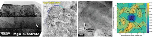
GRAPHICAL ABSTRACT
IMPACT STATEMENT
The innovation of this paper is providing the first plane-view experimental images of in-plane helium precipitate distributions at an interface between physical vapor deposited face-centered cubic (fcc) and body-centered cubic (bcc) metals.
1. Introduction
Physical vapor deposited (PVD) multilayers of face-centered cubic (fcc) and body-centered cubic (bcc) metals have proven to be excellent model materials for studying interactions between solid-state interfaces and radiation-induced defects [Citation1–3]. They have been especially fruitful for investigations of the nucleation, growth, and interaction of helium (He) precipitates at fcc/bcc interfaces [Citation4–7]. To date, however, experimental imaging of He precipitates at these interfaces has been confined to viewing the interfaces edge-on [Citation4–7]. Such imaging reveals the tendency of precipitates to aggregate at interfaces, but does not provide information about the distribution of precipitates within the interface plane. In this paper, we describe the first experimental imaging study of the in-plane distribution of He bubbles at a fcc/bcc interface in a PVD bilayer of copper (Cu) and vanadium (V).
Due to its extremely low solubility [Citation8,Citation9], He is not absorbed into metals from the environment. However, it may be introduced into metals in supersaturated form through nuclear transmutation [Citation10] and decay [Citation11] or through the direct implantation of high-energy He ions [Citation12]. Once inside a metal, He atoms aggregate and grow into nano-scale precipitates or ‘bubbles’ [Citation13]. These bubbles preferentially occupy high-volume [Citation14] or high-energy locations, including interfaces [Citation15]. Understanding the physical mechanisms of interaction between He bubbles and interfaces may shed light on the design of radiation-resistant materials for advanced fission [Citation16] and future fusion [Citation17] reactors.
PVD metal multilayers have been used to study the interaction of He with a variety of interfaces, including Cu–Nb [Citation18–22], Cu–V [Citation6,Citation23], Cu–Mo [Citation24], Al–Nb [Citation25] and Fe–W [Citation26]. Recently, studies on He behavior at interfaces in bulk-scale Cu–Nb nanocomposites synthesized by accumulative roll bonding have also been performed [Citation27,Citation28]. These investigations have generally concluded that He precipitates form preferentially along intrinsic defects within interfaces, such as misfit dislocations and their intersections or interfacial facets [Citation28]. Intrinsic defects are inherent in the internal structure of certain interfaces. They arise directly from the crystallographic character of the interface, i.e. its orientation relation and interface plane orientation [Citation29–31]. For example, previous experiments have found that He bubbles preferentially occupy misfit dislocations intersections (MDIs) [Citation32] on low-angle twist grain boundaries (GBs) in gold (Au).
However, direct observation of the in-plane distribution of He precipitates at fcc/bcc interfaces has proven to be more challenging. The density of intrinsic defects at many of these interfaces is high, making it difficult to distinguish individual defects in transmission electron microscopy (TEM). Correlations between the in-plane distribution of He precipitates in these interfaces and the network of intrinsic interfacial defects have therefore been inferred from indirect experiments [Citation6,Citation20,Citation33,Citation34–36] and atomistic modeling [Citation20,Citation37,Citation38]. We have chosen to investigate He bubble distributions at a Cu/V interface because previous calculations revealed that this interface has a highly anisotropic distribution of misfit dislocations and MDIs [Citation39]. These features enhance the possibility of detecting an anisotropic in-plane distribution of He bubbles decorating intrinsic defects, even if the intrinsic defects themselves cannot be observed [Citation40].
2. Experimental methods
A Cu–V bilayer film was fabricated by election beam evaporation using high-purity (99.999%) Cu and V targets. The vacuum pumping system consisted of a turbomolecular pump backed by a mechanical pump which provided a base pressure of lower than 10−6 mbar. First, a 150 nm thick V film was deposited on a single-crystal MgO(111) substrate at 700°C. Then, the chamber was cooled down to 100°C for the deposition of the Cu film. Elevated temperatures were used during deposition to maximize the diameters of the columnar grains in the deposited film. The deposition rate was set to ∼2 angstroms/s for both the V and Cu layers. The focused ion beam (FIB) lift out technique was applied to prepare both plan view and cross-sectional transmission electron microscopy (TEM) foils. During the process of preparing TEM plan-view foils, the MgO substrate was carefully sputtered away completely. Both microstructure and chemical analysis have been conducted using an FEI Tecnai F30 field emission gun TEM.
Helium ion implantation was conducted at 250°C on a 200 kV Danfysik research ion implanter at the Ion Beam Materials Laboratory at Los Alamos National Laboratory. The TEM samples were mounted on a copper stage using silver paste along with a mechanical clip. The implantation was performed using 30 keV He+ ions to a fluence of 5 × 10¹⁵ ions/cm2 with a flux of ∼2 × 10¹² ions/cm2/s at a temperature of 250°C. The beam direction was perpendicular to the Cu–V interface plane. The stopping and range of ions in matter (SRIM) software was used to calculate the He ion distribution in the Cu–V bilayer film. The peak He concentration was predicted to occur at the Cu/V interface with a concentration of 0.4 at% [Citation41].
3. Results and discussion
(a) shows the morphology of the Cu/V bilayer under strain contrast. Both the Cu and V layers were found to consist of columnar grains with a fiber texture. The diameter of the columnar grains is approximately half a micron in both layers. Isolated grain boundaries, within columns and with planes perpendicular to the Cu/V interfaces, have been detected in the Cu layer (not shown here). These boundaries are Σ3 {112} incoherent twins. (b) shows a selected area electron diffraction (SAED) pattern of the Cu–V film, indicating that the zone axis is along Cu[110] and V[111]. The high-resolution TEM (HRTEM) image ((c)) reveals the interface plane orientations, confirming that the orientation relationship of the Cu/V interface is of the Kurdjumov–Sachs (KS) type: Cu(111)||V(110) and Cu[110]||V[111]. An approximately periodic array of misfit dislocations may be seen near the Cu/V interface. Only dislocations that have an edge component and intersect the image plane may be seen in the figure. They have been marked by red ‘’ symbols. The average distance between them is ∼4 nm. A magnified micrograph of the region highlighted by the yellow dashed box in (c) is presented in (d). A Burgers circuit starting at S and ending at F is shown in (d), demonstrating a closure failure of aCu/6[112].
Figure 1. (a) Cross-sectional TEM micrograph of a Cu–V bilayer film deposited on an MgO substrate. (b) Corresponding diffraction pattern showing that the following crystallographic directions are parallel within the interface planes: Cu[110]||V[111]||MgO[110]. (c) Atomic structure of the interface showing that the interface plane is parallel to Cu(111) and V(110) planes. Interface misfit dislocations that contain an edge component and intersect the image plane are marked by red ‘⊥’ symbols. (d) Magnified image of the yellow dashed box in (c).
![Figure 1. (a) Cross-sectional TEM micrograph of a Cu–V bilayer film deposited on an MgO substrate. (b) Corresponding diffraction pattern showing that the following crystallographic directions are parallel within the interface planes: Cu[110]||V[111]||MgO[110]. (c) Atomic structure of the interface showing that the interface plane is parallel to Cu(111) and V(110) planes. Interface misfit dislocations that contain an edge component and intersect the image plane are marked by red ‘⊥’ symbols. (d) Magnified image of the yellow dashed box in (c).](/cms/asset/f3530ea0-255e-458a-9e69-fa2cf3c58f22/tmrl_a_1287132_f0001_c.jpg)
A plan-view dark field scanning TEM (STEM) micrograph of the as-deposited Cu/V sample is presented in (a). We used energy-dispersive spectroscopy to confirm that all of the MgO substrate was removed from this sample: only Cu and V signals were detected during this analysis. The contrast distribution in (a) reveals that there are two grains in the image. The boundaries between them have been labeled with dashed lines, with blue color representing Cu⟨110⟩ directions and bright blue representing Cu⟨112⟩. The zone axis is Cu⟨111⟩. Thus, the boundaries labeled with the blue-dashed lines are Σ3{112} incoherent twin boundaries, which are commonly encountered in PVD Cu layers.
Figure 2. (a) Plan-view TEM image of an as-deposited Cu/V bilayer showing slip steps created at the Cu/V interface by threading dislocations. (b) Schematic diagram of the orientation of (111) glides planes in the Cu film relative to the Cu/V interface.
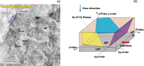
Dislocation lines appear bright in dark field imaging. Several curved white lines may be seen inside Grain II in (a). We interpret these lines as threading dislocations within the Cu layer: dislocations that propagate parallel to the free surface and interface planes, relaxing growth stresses in the film [Citation42]. Another clear contrast feature in (a) is the network of straight black lines in Grain II. These networks are composed of two sets of lines at 60 degree angles to each other. Distances between two neighboring parallel black lines vary between ∼10 and ∼30 nm.
This network pattern is not consistent with the orientation and spacing of misfit dislocations at the Cu/V interface. More likely, it consists of atomic-size steps deposited on the Cu/V interface by threading dislocations traveling through the Cu layer. In Cu, dislocations glide along {111}-type planes. The schematic in (b) shows the orientation of three such planes intersecting the Cu/V interface in a Cu layer with the crystallographic orientation observed in our sample. The electron beam is directed along the z-axis in this schematic. The intersections of these planes with the Cu/V interface form lines along Cu⟨110⟩ type directions at angles of 60 degrees to each other, in agreement with (a).
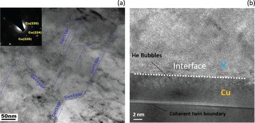
(a) and (b) illustrate He bubble distributions in the He-implanted plan view and cross-sectional samples, respectively. Numerous nanoscale bubbles with a diameter of approximately 3–5 nm were observed in both samples. He bubbles exhibit a clear tendency to align along grain boundaries. In addition, there also appears to be a tendency for bubbles to align along Cu⟨110⟩ crystallographic directions, as indicated by blue dashed lines in (a). The cross-sectional high-resolution TEM image in (b) shows individual helium bubbles located within the Cu layer and contacting the Cu/V interface.
Figure 3. (a) Plan-view TEM image of helium implanted Cu/V foil, taken with under-focus of 400 nm. Helium bubbles appear to align preferentially at grain boundaries and along Cu⟨110⟩-type crystallographic directions. (b) Edges of He bubbles at the Cu/V interface imaged by high-resolution TEM, taken with under-focus of 200 nm.
Additional quantitative information may be extracted through digital analysis of the under-focused and over-focused TEM micrographs shown in (a, b), respectively. In the former, helium bubbles appear as light spots while in the latter they appear as dark spots. Since the background contrast in both images is comparable, we may subtract them from each other to obtain an image containing only the bubbles themselves, as shown in (c). This image was analyzed using MATLAB to extract the locations and radii of all bubbles. (d) shows a digital plot of the data obtained with bubble areas exaggerated by a factor of five for clarity.
Figure 4. (a) Under-focused and (b) over-focused plan-view TEM micrographs of a He-implanted Cu/V bilayer, taken with defocusing of minus and plus 400 nm respectively. (c) An image generated by subtracting (b) from (a). The plot of the digitized He bubble positions obtained from (c) is given in (d). Bubble areas in (d) are exaggerated by a factor of five for clarity. The red circles illustrate regions that do not contain GBs decorated by He atoms. Bubbles drawn from these regions are used for the statistical analysis described in the text.
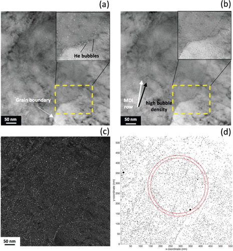
Some of the helium bubbles in exhibit an evident tendency to aggregate into ordered arrangements. For instance, as in (a), bubbles preferentially decorate the GB indicated in (a). Inspection of the vicinity of this GB in (d) suggests that the GB is furthermore flanked on both sides by zones with reduced helium bubble concentration. In addition to these prominent arrangements along GBs, He bubbles that are far from GBs may also exhibit subtler forms of ordering. We carried out a statistical analysis of the digitized atom positions shown in (d) to search for such aggregation tendencies. To exclude bubbles decorating GBs, we restricted these analyses to bubbles within the two red circles shown in (d).
(a) presents a distribution of radii for bubbles contained within the larger red circle in (d) (1597 bubbles total). The distribution is narrow, falling off rapidly to zero below a radius of ∼0.5 nm and above ∼1 nm. It has a mean of ∼0.6 nm. Because of the Fresnel contrast of the bubbles at the 400 nm under-focus condition, these values may overestimate the true radius by as much as ∼ 20% [Citation43]. (b) plots pair distribution functions as a function of distance between bubbles computed using three different bin numbers. To avoid sampling artifacts, the center position bubbles in this calculation were drawn from the smaller circle in (d) (1351 bubbles total) while the neighbors of these atoms were drawn from the larger circle. The difference in radius between these circles is ∼13.7 nm: equal to the maximum bubble-to-bubble distance plotted in (b). At large inter-bubble distances, all three distribution functions converge to the same average bubble density of ∼0.0225/nm2. Because the TEM foil is ∼ 100 nm thick, the corresponding volume density is ∼2.25 × 10²³/m3. At low distances, all three functions exhibit a reduced bubble density, demonstrating that bubbles are not distributed randomly. Rather, each bubble is surrounded by an ‘exclusion zone’: the presence of a bubble at one location reduces the likelihood of finding another bubble at a location within a surrounding region of a radius ∼4 nm.
Figure 5: (a) Distribution of bubble radii. (b) Bubble pair distribution function as a function of distance between bubbles. (c) Bubble pair distribution function expressed in terms of the x- and y-positions of bubbles neighboring a central bubble.
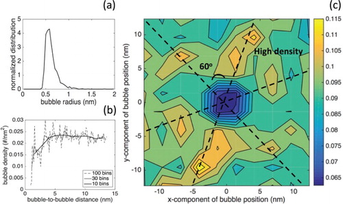
Finally, using the same sampling strategy as employed in (b), we computed a pair distribution function that tracks not just the bubble-to-bubble distance, but also the x- and y-coordinates of bubbles neighboring the central bubble. The outcome is shown in (c). As expected, this 2-D pair distribution also exhibits an exclusion zone: a region of reduced bubble density approximately 4 nm in radius surrounding the central bubble. Moreover, this distribution is clearly anisotropic: an elevated density of bubbles is aligned along the three ‘high-density’ lines with angles of 60 degrees between them, as plotted in (c). Approximately mid-way between them lie three ‘low-density’ directions.
This anisotropic bubble distribution cannot be attributed to helium bubbles decorating GBs, as these were intentionally excluded from the calculation that resulted in (c), as described above. Neither the shape nor the orientation of such a pattern can match the calculated distribution of misfit dislocation intersections (MDIs) in the KS Cu/V interface, either. (b) illustrates the discrepancy between the direction of preferential alignment of He bubbles and the direction of closest MDI spacing in the Cu/V interface.
However, the directions of preferential He bubble alignment shown in (c) are consistent with Cu⟨110⟩-type directions, as proposed previously. As illustrated in , slip steps deposited along Cu/V interfaces by threading dislocations also lie along Cu⟨110⟩-type directions. We therefore conclude that He bubbles preferentially decorate these slip steps, rather than intrinsic interfacial defects. Current TEM imaging techniques are not able to determine whether individual He bubbles lie along individual slip steps, so our conclusion remains an inference based on comparison of as-deposited and He-implanted samples.
Finally, we observed one isolated case—shown in (a)—of helium bubbles aligning along directions that are not Cu⟨110⟩-type directions. (b) shows a magnified view of this arrangement, highlighting groups of bubbles aligned into rows marked by red dashed lines. The distance between two adjacent rows of these helium bubbles is ∼8 nm. Within each row, bubbles have an average spacing of ∼2 nm, with no two neighboring bubbles overlapping each other. To check whether these bubbles may be decorating MDIs, we calculated distributions of MDIs at a Cu/V KS interface using O-lattice theory, as described in [Citation34]. We used cubic lattice parameters for Cu and V of aCu = 0.36 nm and aV = 0.30 nm, respectively, and found that the shortest distance between MDIs is lmin = 2.2 nm and the perpendicular distance between rows of closest-spaced MDIs is l⊥ = 8.4 nm, similar to the rows of bubbles in (c). The predicted direction of closest MDI spacing is not aligned with any low index crystallographic direction in Cu or V. In fact, this direction is rotated by approximately 14° from the ⟨112⟩fcc and ⟨112⟩bcc directions within the interface plane, as shown in (c).
Figure 6. (a) Plan-view TEM image of aligned He bubbles, taken with under-focus of 400 nm; (b) magnified image of the yellow dashed box in (a); and (c) schematic diagram of MDIs at a Cu/V interface with KS orientation relationship.
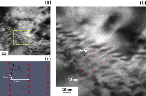
Although the exact crystallographic orientation of the bubble alignment in is uncertain, the spacing between these bubbles is close to the calculated MDI pattern. Thus, it seems plausible that these bubbles are formed at the intersection points of misfit dislocations. If so, then the present observations would be the first time such an ordered He distribution pattern has been directly imaged at a fcc/bcc interface. He bubble networks on misfit dislocation intersections have been observed previously at low-angle twist GBs in Au [Citation32]. At present, we cannot exclude the possibility that the pattern in may have formed along a different kind of defect structure, e.g. along a low-angle tilt GB passing through the Cu layer. However, since such GBs have not been previously reported in PVD-deposited Cu layers, it seems that the likelihood of encountering such a GB here is low.
4. Conclusions
We have presented TEM images of helium bubble distributions within the plane of a Cu/V interface. Detailed analysis of these images reveals a tendency for helium bubbles to decorate atomic steps created along the interface by threading dislocations. Certain bubble patterns are also consistent with the distribution of misfit dislocation intersections predicted by O-lattice theory for Cu/V interfaces in the Kurdjumov–Sachs orientation relation. Our work provides the first direct, plan-view images of He bubble distributions at interfaces between fcc and bcc metals.
Acknowledgements
We are grateful to M. Seita for performing the image subtraction as well as bubble radius and location identification shown in . Part of the research was performed at the Center for Integrated Nanotechnologies, an Office of Science User Facility operated for the U.S. Department of Energy (DOE) Office of Science. Los Alamos National Laboratory is operated by Los Alamos National Security, LLC, for the National Nuclear Security Administration of the U.S. Department of Energy under Contract No. DE-AC52-06NA25396.
Disclosure statement
No potential conflict of interest was reported by the authors.
Additional information
Funding
References
- Misra A, Demkowicz MJ, Zhang XH, Hoagland RG. The radiation damage tolerance of ultra-high strength nanolayered composites. JOM. 2007;59:62–65. doi: 10.1007/s11837-007-0120-6
- Beyerlein IJ, Demkowicz MJ, Misra A, Uberuaga BP. Defect-interface interactions. Prog Mater Sci. 2015;74:125–210. doi: 10.1016/j.pmatsci.2015.02.001
- Demkowicz MJ, Bellon P, Wirth BD. Atomic-scale design of radiation-tolerant nanocomposites. MRS Bulletin. 2010;35(12):992–998. doi: 10.1557/mrs2010.704
- Callisti M, Karilik M, Polcar T. Bubbles formation in helium ion irradiated Cu/W multilayer nanocomposites: Effects on structure and mechanical properties. J Nucl Mater. 2016;473:18–27. doi: 10.1016/j.jnucmat.2016.02.006
- Fu EG, Wang H, Carter J, Shao L, Wang YQ, Zhang X. Fluence-dependent radiation damage in helium (He) ion-irradiated Cu/V multilayers. Philos Mag. 2013;93(8):883–898. doi: 10.1080/14786435.2012.735773
- Li N, Nastasi M, Misra A. Defect structures and hardening mechanisms in high dose helium ion implanted Cu and Cu/Nb multilayer thin films. Int J Plasticity. 2013;32–33:1–16. doi: 10.1016/j.ijplas.2011.12.007
- Gao Y, Yang TF, Xue JM, Yan S, Zhou SQ, Wang YG, Kwok TK, Chu PK, Zhang YW. Radiation tolerance of Cu/W multilayered nanocomposites. J Nucl Mater. 2011;413(11):11–15. doi: 10.1016/j.jnucmat.2011.03.030
- Laakmann J, Jung P, Uelhoff W. Solubility of helium in gold. Acta Matallurgica. 1987;35(8):2063–2069. doi: 10.1016/0001-6160(87)90034-4
- Lamdolt H, Ehrhart P, Ullmaier H. Atomic defects in metals. Berlin: Springer-Verlag; 1991.
- Ullmaier H. The influence of helium on the bulk properties of fusion reactor structural materials. Nuclear Fusion. 1984;24(8):1039–1083. doi: 10.1088/0029-5515/24/8/009
- Coltman RR, Klabunde CE, Mcdonald DL, Redman JK. Reactor damage in pure metals. J Appl Phys. 1962;33:3509–3522. doi: 10.1063/1.1702438
- Gadalla AA, Jager W, Ehrhart P. TEM investigation of the microstructural evolution during MEV helium implantation in copper. J Nucl Mater. 1985;137(1):73–76. doi: 10.1016/0022-3115(85)90051-0
- Rothaut J, Schroeder H, Ullmaier H. The growth of helium bubbles in stainless steel at high temperatures. Philos Mag A. 1983;47(5):781–795. doi: 10.1080/01418618308245265
- Xu WZ, Li LL, Valdez JA, Saber M, Zhu YT, Carl C, Koch CC, Scattergood RO. Effect of nano-oxide particle size on radiation resistance of iron–chromium alloys. J Nucl Mater. 2016;469:72–81. doi: 10.1016/j.jnucmat.2015.11.044
- Kesternich W. Helium trapping at dislocations, precipitates and grain boundaries. Radiation Effects. 1983;78(1–4):261–273. doi: 10.1080/00337578308207376
- Beyerlein IJ, Caro A, Demkowicz MJ, Mara NA, Misra A. Radiation damage tolerant nanomaterials. Materialstoday. 2013;16(11):443–449.
- Hasegawa A, Kohyama A, Jones RH, Snead LL, Riccardi B, Fenici P. Critical issues and current status of SiC/SiC composites for fusion. J Nucl Mater. 2000;283–287:128–137. doi: 10.1016/S0022-3115(00)00374-3
- Hochbauer T, Misra A, Hattar K, Hoagland RG. Influence of interfaces on the storage of ion-implanted He in multilayered metallic composites. Appl Phys. 2005;98:123516. doi: 10.1063/1.2149168
- Zhang X, Li N, Anderoglu O, Wang H, Swadener JG, Hochbauer T, Misra A, Hoagland RG. Nanostructured Cu/Nb multilayers subjected to helium ion-irradiation. Nucl Instrum Methods Phys Res Sect B. 2007;261(1–2):1129–1132. doi: 10.1016/j.nimb.2007.03.098
- Demkowicz MJ, Bhattacharyya D, Usov I, Wang YQ, Nastasi M, Misra A. The effect of excess atomic volume on He bubble formation at fcc-bcc interfaces. A Appl Phys Lett. 2010;97:161903. doi: 10.1063/1.3502594
- Han WZ, Mara NA, Wang YQ, Misra A, Demkowicz MJ. He implantation of bulk Cu–Nb nanocomposites fabricated by accumulated roll bonding. J Nucl Mater. 2014;452:57–60. doi: 10.1016/j.jnucmat.2014.04.034
- Li N, Mara N, Wang YQ, Nastasi M, Misra A. Compressive flow behavior of Cu thin films and Cu/Nb multilayers containing nanometer-scale helium bubbles. Scripta Mater. 2011;64:974–977. doi: 10.1016/j.scriptamat.2011.02.001
- Fu EG, Misra A, Wang H, Shao L, Shang X. Interface enabled defects reduction in helium ion irradiated Cu/V nanolayers. J Nucl Mater. 2010;407(3):178–188. doi: 10.1016/j.jnucmat.2010.10.011
- Li N, Carter JJ, Misra A, Shao L, Wang H, Zhang X. The influence of interfaces on the formation of bubbles in He-ion-irradiated Cu/Mo nanolayers. Philos Magazine Lett. 2011;91:18–28. doi: 10.1080/09500839.2010.522210
- Li N, Martin MS, Anderoglu O, Misra A, Shao L, Wang H, Zhang X. He ion irradiation damage in Al/Nb multilayers. J Appl Phys. 2009;105:123552.
- Li N, Fu EG, Wang H, Carter JJ, Shao L, Maloy SA, Misra A, Zhang X. He ion irradiation damage in Fe/W nanolayer films. J Nucl Mater. 2009;389(2):233–238. doi: 10.1016/j.jnucmat.2009.02.007
- Han WZ, Demkowicz MJ, Nathan AM, Fu EG, Sinha S, Rollett AD, Wang YQ, Captenter JS, Beyerlein IJ, Misra A. Design of radiation tolerant materials via interface engineering. Adv Mater. 2013;25(48):6975–6979. doi: 10.1002/adma.201303400
- Timothy GL, Elvan HE, Robert SA, Nathan AM, Pascal B. Role of interfaces on the trapping of He in 2D and 3D Cu–Nb nanocomposites. J Nucl Mater. 2015;466:36–42. doi: 10.1016/j.jnucmat.2015.07.020
- Wei QM, Misra A. Transmission electron microscopy study of the microstructure and crystallographic orientation relationships in V/Ag multilayers. Acta Matallurgica. 2010;58(14):4871–4882.
- Singh BN, Leffers T, Green WV, Victoria M. Nucleation of helium bubbles on dislocations, dislocation networks and dislocations in grain boundaries during 600 MeV proton irradiation of aluminium. J Nucl Mater. 1984;125:287–297. doi: 10.1016/0022-3115(84)90556-7
- Thorsen PA, Bilde-Sorensen JB, Singh BN. Influence of grain boundary structure on bubble formation behaviour in helium implanted copper. Mater Sci Forum. 1996;207–209:445–448. doi: 10.4028/www.scientific.net/MSF.207-209.445
- Di Z, Bai XM, Wei Q, Won J, Hoagland RG, Wang Y, Misra A, Uberuaga BP, Nastasi M. Tunable helium bubble superlattice ordered by screw dislocation network. Phys Rev B. 2011;84:052101. doi: 10.1103/PhysRevB.84.052101
- Demkowicz MJ, Misra A, Caro A. The role of interface structure in controlling high helium concentrations. Curr Opin Solid State Mater Sci. 2012;16:101–108. doi: 10.1016/j.cossms.2011.10.003
- Kashinath A, Wang P, Majewski J, Baldwin JK, Wang YQ, Demkowicz MJ. Detection of helium bubble formation at fcc-bcc interfaces using neutron reflectometry. J Appl Phys. 2013;114:043505. doi: 10.1063/1.4813780
- Zhernenkov M, Jablin MS, Misra A, Nastasi M, Wang YQ, Demkowicz MJ, Baldwin JK, Majewski J. Trapping of implanted He at Cu/Nb interfaces measured by neutron reflectometry. Appl Phys Lett. 2011;98:241913. doi: 10.1063/1.3600642
- Zhernenkov M, Gill S, Stanic V, DiMasi E, Kisslinger K, Baldwin JK, Misra A, Demkowicz MJ and Ecker L. Design of radiation resistant metallic multilayers for advanced nuclear systems. Appl Phys Lett. 2014;104:241906. doi: 10.1063/1.4883481
- Kashinath A, Misra A, Demkowicz MJ. Stable storage of helium in nanoscale platelets at semicoherent interfaces. Phys Rev Lett. 2013;110:086101. doi: 10.1103/PhysRevLett.110.086101
- Zhang X, Fu EG, Misra A, et al. Interface-enabled defect reduction in He ion irradiated metallic multilayers. JOM. 2010;62:75–78. doi: 10.1007/s11837-010-0185-5
- Yuryev DV, Demkowicz MJ. Computational design of solid-state interfaces using O-lattice theory: An application to mitigating helium-induced damage. Appl Phys Lett. 2014;105:221601. doi: 10.1063/1.4902888
- Yuryev DV, Demkowicz MJ. Modeling growth, coalescence, and stability of helium. precipitates on patterned interfaces. Modeling Simul Mater Sci Eng. 2016;25:015003. doi: 10.1088/0965-0393/25/1/015003
- Ziegler JF, Ziegler MD, Biersack JP. SRIM–The stopping and range of ions in matter. Nucl Instrum Methods Phys Res Sect B. 2010;268:1818–1823. doi: 10.1016/j.nimb.2010.02.091
- Matthews JW, Blakeslee AE. Defects in epitaxial multilayers: II. Dislocation pile-ups, threading dislocations, slip lines and cracks. J Crystal Growth. 1975;29(3):273–280. doi: 10.1016/0022-0248(75)90171-2
- Wei QM, Li N, Mara N, Nastasi M, Misra A. Suppression of irradiation hardening in nanoscale V/Ag multilayers. Acta Matallurgica. 2011;59(16):6331–6340.