
ABSTRACT
Nanocrystalline metals are considered highly radiation-resistant materials due to their large grain boundary areas. Here, the existence of a grain size threshold for enhanced irradiation resistance in high-temperature helium-irradiated nanocrystalline and ultrafine tungsten is demonstrated. Average bubble density, projected bubble area and the corresponding change in volume were measured via transmission electron microscopy and plotted as a function of grain size for two ion fluences. Nanocrystalline grains of less than 35 nm size possess ∼10–20 times lower change in volume than ultrafine grains and this is discussed in terms of the grain boundaries defect sink efficiency.
GRAPHICAL ABSTRACT
IMPACT STATEMENT
A grain size threshold in nanocrystalline and ultrafine tungsten has been shown to exist for enhanced irradiation-resistance performance during high-temperature helium irradiation.
Grain size refinement is proposed as a solution for enhanced radiation tolerance in materials under extreme irradiation conditions due to the high grain boundary density it can induce [Citation1]. Grain boundaries which act as defect [Citation2] and particle (e.g. helium, He) [Citation3] sinks are also postulated to enhance vacancy-interstitial annihilation [Citation4]. This can lead to a decrease in defect (e.g. interstitial clusters, bubbles, voids, etc.) density and thus to an enhancement of the irradiation resistance of the microstructure. Tungsten (W), which is an important material for the major components of several nuclear fusion systems including the divertor region in ITER [Citation5], is an example of a material in which grain size refinement can significantly enhance its performance [Citation6]. When exposed to He irradiation at high temperatures, W has been shown to suffer from high He bubble densities in the grain matrices [Citation7]. Over an ion dose threshold, this is considered to be the main phenomenon responsible for severe microstructural changes and the formation of fuzz (fiberform morphology) which occur at high ion doses [Citation7]. If a major driver for these microstructural changes is indeed the high bubble densities in the grain matrices as has been suggested [Citation8], it can then be hypothesized that the high grain boundary area in a nanocrystalline W microstructure will increase the ion dose threshold required to form these microstructures at temperatures where no grain growth (which changes sink strength) is possible.
To correlate the nanoscale phenomena of bubble evolution to microscale structural changes such as fuzz formation, fundamental studies regarding bubbles in grain-refined W are essential to understand the role of grain boundaries in limiting bubble densities in the grain matrices. El-Atwani et al. [Citation9] have demonstrated preferential bubble formation on the grain boundaries in nanocrystalline W grains and lower bubble densities in their matrices. Investigations are required on grain-refined (nanocrystalline (<100 nm) and ultrafine (100–500 nm)) W to explore possible trends in bubble density as a function of grain size and the grain size threshold required to achieve significantly lower bubble densities in the grain matrices. Moreover, since the average bubble size may also change as a function of grain size, the total volume of the bubbles (which we equate to change in grain volume as discussed below) is a more effective indicator for the performance of a grain compared to bubble density alone.
In this study, we attempt to answer the above questions using in situ ion irradiation of nanocrystalline and ultrafine tungsten (where nanocrystalline and ultrafine grains coexist) within the JEOL JEM-2000FX transmission electron microscope (TEM) at the Microscope and Ion Accelerator for Materials Investigations (MIAMI) facility at the University of Huddersfield which is described in detail elsewhere [Citation10]. The in situ observation during the experiment confirmed that the sample was irradiated uniformly and that no grain growth or bubble coalescence occurred during irradiation; two possible phenomena that can disturb bubble density and size determination. High-purity (99.95% wt%) W samples containing both ultrafine and nanocrystalline grains were irradiated with 2 keV He ions at 950°C to two different ion fluences of 3.6 × 10¹⁹ and 3.2 × 10²⁰ ions m−2 (flux was approximately 1.8 ×10¹⁷ ions m−2 s−1). Preparation of ultrafine and nanocrystalline W material and the TEM samples (via electropolishing) has been detailed elsewhere [Citation11,Citation12].
Ex situ TEM was performed using a JEOL JEM-3010 and an FEI-TECNAI-20 with electron beam energies of 300 and 200 keV, respectively. Images were captured in underfocus conditions in which cavities are visible with a bright Fresnel fringe on their inside edge. At the angle of incidence of 60° between the ion beam and the sample surface at 0° tilt, the projected range for 2 keV He ions in W is 10.6 nm as calculated by the ‘detailed calculation with full damage cascade’ option in the Monte Carlo computer code Stopping Range of Ions in Matter (SRIM version 2013) [Citation13]. The projected range is therefore much less than the nominal thickness of the film of about 100 nm. This is an important consideration to be sure that all the helium is stopped in the grains and also when comparing phenomena such as bubble formation which can be affected by the proximity to free surfaces in the foil. The TEM images were then used to determine the bubble areal number density (henceforth referred to as bubble density) and projected area of the bubbles as a function of grain size. Grain size was measured as the minimum distance across a grain through the point inside the grain farthest from any grain boundaries. Grain volume was calculated by measuring the projected area of the grain and multiplying by a nominal sample thickness of 100 nm. Details about He bubble quantification and possible factors affecting bubble density measurements were illustrated in a previous work regarding He irradiation on nanocrystalline iron [Citation14].
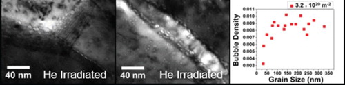
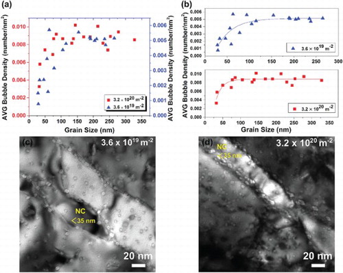
The performance of the refined grains under irradiation in terms of bubble formation is illustrated in the plots in Figure . Bubble density as a function of grain size in the ultrafine and nanocrystalline regimes is plotted for the two ion fluences used. In the plots, the bubbles judged to be on the grain boundaries were not considered. To the best of our knowledge, the effect of grain boundary bubbles on swelling is still not reported. Moreover, several factors (such as defect accommodation in the grain boundary free volume, bubble densities on different grain boundaries and possible void-grain boundary pinning during the volumetric change) need to be understood to quantify the effect of grain boundary bubbles on swelling. However, bubbles on all regions of the grains except the denuded zones (bubble-free regions) were considered. Results from the post-irradiation analysis of the two different ion fluences showed a very similar trend (Figure (a)) demonstrating no effect of ion fluence on the response of the nanocrystalline grains in this range. The bubble density vs grain size trend also demonstrates how sink strength (proportional to grain boundary area per unit of grain volume) [Citation15] affects the performance of grains as regards to bubble formation in the grain matrices. The bubble density increased in a logarithmic fashion with grain size up to 75–100 nm where it increased at a slower rate and eventually reached a saturation value. The saturation value, however, was different for the two ion fluences (0.005 and 0.009 bubble nm−2) for 3.6 × 10¹⁹ and 3.2 × 10²⁰ ions m−2, respectively). Grains with of a size of less than 35 nm demonstrated the lowest bubble densities of up to approximately 10 and 3 times lower than the saturation values for the ion doses of 3.6 × 10¹⁹ and 3.2 × 10²⁰ ions m−2, respectively. The bubble density results can be affected by the surface sink effects. However, surface effects are expected to play a more significant role in large grains due to the longer diffusion path of the defects to the grain boundaries. In our results, we observe larger bubble densities in the matrices of the large grains than those in the small grains which confirms that surface sink effects do not dominate in this experiment and the enhanced performance of the small grains. The scatter in the data (i.e. similarly sized grains with different bubble densities) has been observed before in He ion-irradiated iron and were explained by El-Atwani et al. [Citation14] in terms of grain boundary sink efficiency and its dependent parameters. Under the irradiation conditions in this study, both interstitial and vacancy defects are created and can migrate [Citation16]. Moreover, vacancy clusters and small He-vacancy complexes [Citation17] can also migrate to the boundaries [Citation18]. The sink efficiency of a grain boundary, however, was shown by others to depend on the full grain boundary character (including the misorientation angle and the grain boundary plane) [Citation19]. Therefore, grains with different grain boundaries can have different bubble densities due to the different sink efficiencies of their boundaries. Figure (c,d) shows bright-field underfocus TEM images typical of the two ion-irradiated fluences studied. Nanocrystalline grains clearly demonstrated lower bubble densities than adjacent ultrafine grains.
Figure 1. Plots of (a) average bubble density (number/nm2) vs grain size for the two different ion fluences showing a very similar trend; and (b) bubble density (number/nm2) vs grain size for the two different ion fluences with exponential decay fitting. (Fitting curves are and
for the 3.6 × 10¹⁹ and 3.2 × 10²⁰ ions m−2, respectively. Bright-field underfocus TEM images showing: nanocrystalline (NC) grains of size less than 35 nm adjacent to larger grains for (c) 3.6 × 10¹⁹ and (d) 3.2 × 10²⁰ ions m−2.
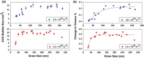
Bubble density is not sufficient on its own to characterize the bubble populations in the irradiated grains as bubble size must also be taken into account. In this study, the microstructural changes were characterized in terms of these bubbles and the change in grain volume they are taken to represent. The change in microstructure, in this study, is characterized by the change in volume due to bubble formation observed in the Fresnel TEM images. The relative volume change is found by [Citation20]
where Δv is the change in volume of the grain, v is the volume of the grain, Nv is the bubble density per unit volume (bubble areal density divided by the sample thickness) and rc is the average radius of the bubbles in the grain. Figure (a) shows the average bubble size vs grain size for both ion fluences. Small grains of less than 35 nm demonstrate the smallest average bubble sizes. The scatter in the average bubble size data can be explained using the sink efficiency arguments discussed above. The change in grain volumes was calculated using the bubble densities shown in Figure and rc was calculated from the average bubble sizes. The relative changes in volume are plotted in Figure (b). An exponential decay of Δv/v as a function of grain size is evident with the grains of less than 35 nm having the smallest relative changes in volume. For the lower ion fluence, the smallest relative change in volume was approximately nine times less than the saturation value of approximately 0.022 bubble nm−2; for the higher ion fluence, the smallest relative change in volume was approximately 24 times less than the saturation value of approximately 0.06 bubble nm−2.
Figure 2. Plots showing (a) average bubble area (nm2) as a function of grain size for the two fluences; and (b) relative change in volume (Δv/v) for the two samples as a function of grain size with exponential decay fitting. (Fitting curves are and
for the 3.6 × 10¹⁹ and 3.2 × 10²⁰ ions m−2, respectively. Error bars in the average bubble size graph represent the standard error of the mean.
In the grain size regime of less than 35 nm, it is evident that a nanocrystalline grain in the higher dose sample can have a comparable bubble density, size and change in volume to a similar grain size in the lower dose sample despite being irradiated to a 10 times higher ion dose. This can be related to the sink efficiency of the boundaries and the low diffusion length for defects (including He-vacancy complexes) in those grains. Below a grain size threshold which was found to be around 35 nm under the experimental conditions in this study, the grain boundaries appear to absorb a significant proportion of the mobile defects from the grain sufficient to have a substantial impact on bubble formation within the grain. Therefore, it is concluded that these observations demonstrate efficient defect absorption by the grain boundaries and that this has significant implications for the evolution of bubbles in the nanocrystalline grains and especially in grains smaller than 35 nm. However, the deviation of the grain size threshold as a function of temperature is an important factor to consider and is yet to be studied. At the irradiation conditions in this work, vacancies, interstitials and small He-vacancy clusters are mobile. Therefore, grain boundaries can play a dominant role in defect absorption and annihilation and a grain size threshold can be identified. A similar grain size threshold has also been identified in BCC Fe material [Citation24] at conditions where defects are mobile. Moreover, while the higher fluence was around one order of magnitude greater than the lower fluence studied, the bubble density-to-relative-volume-change-saturation ratios were approximately 1.8 and 2.7, respectively. A few possible explanations can help to explain this observation. The irradiations were performed with 2 keV helium ions which is higher than the displacement energy threshold of around 500 eV in W [Citation21]. Therefore, vacancy supply to bubbles is always possible and thus over-pressurized bubbles do not form [Citation22]. The He-to-vacancy ratio in the bubbles of the irradiated samples can then be different (larger for the higher fluence). Moreover, in the higher fluence case, it is expected that higher interstitial loop and dislocation densities will be able to more efficiently trap He atoms [Citation23]. Nucleation of small bubbles on dislocations under similar irradiation conditions has been reported in the literature [Citation9] confirming the He trapping behavior of dislocations. However, it is expected that the dominant factor is the efficient absorption of defects by grain boundaries as supported by the high number of large bubbles observed on the grain boundaries. Grain boundary absorption of vacancies, vacancy clusters and He-vacancy complexes can result in reduced bubble densities as it is the agglomeration of these smaller defects which leads to the nucleation of the bubbles. This is reflected by the larger densities and bubble sizes on most of the grain boundaries of the higher dose sample as observed in many TEM micrographs. An example is shown in Figure (a,b). It should be noted that bubble densities and average sizes on the grain boundaries are not uniform but this is to be expected as different grain boundaries are known to have different sink efficiencies [Citation19] as discussed above. The formation of a non-uniform distribution of large bubbles on the grain boundaries observed in this work has also been seen on other materials irradiated with He [Citation24].
Figure 3. Bright-field underfocus TEM micrographs showing (a) and (b) samples irradiated to 3.6 × 10¹⁹ and 3.2 × 10²⁰ ions m−2, respectively, demonstrating the difference in bubble density and size at the grain boundaries (GB); and (c) a sample irradiated to 3.2 × 10²⁰ ions m−2 showing several grain boundaries decorated with different densities, shapes and sizes of bubbles. Please note the different scale in (a) and (b) compared to (c).
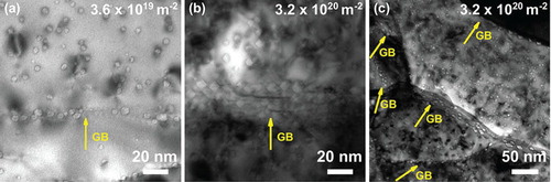
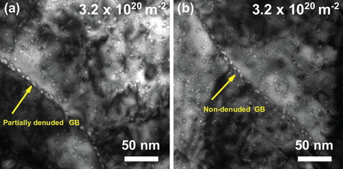
As can be seen from Figures , and , many bubbles on the grain boundaries were facetted. The faceting of cavities has been demonstrated to occur when a cavity becomes sufficiently large such that it can minimize its surface energy by diverging from a spherical shape [Citation25]. Therefore, these facetted bubbles are further evidence of significant vacancy trapping by the grain boundaries and it is reasonable to assume similar efficiency for coincident trapping of helium. The difference in sink efficiencies of different grain boundaries can also be experimentally confirmed by the observation of denuded zones (a bubble-free region in the vicinity of a boundary) as the width of the denuded zone is directly proportional to the grain boundary sink efficiency [Citation26]. In the current study, the regions around grain boundaries demonstrated inconsistent behavior with some being denuded and some only partially denuded. Figure shows examples of denuded and partially denuded zones along grain boundaries pointing to the differing sink efficiencies of the bordering grain boundaries.
Figure 4. Bright-field underfocus TEM micrographs showing (a) the partially denuded and (b) the non-denuded grain boundaries at a fluence of 3.2 × 10²⁰ ions m−2.
The performance of nanocrystalline and ultrafine W at low fluences can assist in understanding the changes in morphology such as fuzz formation observed at larger scales. This is evidenced by the finding here that similar bubble densities, average bubble sizes and change in volume trends exist at very different fluences differing by more than one order of magnitude. It is clear that nanocrystalline grains below a size threshold are more tolerant to intra-grain bubble formation compared to ultrafine grains. The threshold values identified in the bubble density and the volume change plots shown in Figure correspond to grains in the ultrafine regime. A comparison with coarse-grained W is unfortunately not currently possible as no data exist yet on bubble density as a function of grain size in the fine regime (>500 nm). However, as the grain size in coarse-grained W is above the threshold grain size identified here, it is reasonable to assume that it would behave similarly to the ultrafine-grained W. Assuming that the hypothesis that fuzz formation is correlated with high bubble densities in the matrix as proposed by Kajita et al. [Citation8] is correct and neglecting other possible effects (such as defect and bubble-induced stresses [Citation27,Citation28]), it may be conjectured that a W sample of 35 nm grains may be able to resist fuzz formation to an ion fluence at least one order of magnitude greater than a sample of ultrafine or fine W based on the results reported here. Indeed, recently a sample of nanocrystalline and ultrafine W was demonstrated to have an order of magnitude greater threshold for fuzz formation when compared to coarse-grained W [Citation6].
While it is promising that bubble density and change-in-volume trends can be controlled by the engineering of grain size, the high density of large bubbles on the grain boundaries is of concern. Since the mechanical properties of nanocrystalline materials are dominated by the grain boundaries [Citation29], the decoration of these by cavities may degrade performance and a tradeoff grain size or grain size distribution may have to be reached or other methods of limiting bubble nucleation and growth should be developed such as the addition of impurities or formation of tungsten alloys. Bubbles can nucleate through the growth of He-vacancy complexes [Citation30]. Impurities are previously discussed to have several effects in helium-irradiated materials such as trapping interstitial helium (decreasing nucleation sites), enhancing recombination by trapping point defects and impurity segregation to grain boundaries which alters their sink efficiency [Citation31]. Impurities can also inhibit bubble migration and clustering [Citation32]. The results in the work can act as a reference for forthcoming studies on irradiation resistance of nanocrystalline tungsten alloys.
In summary, bubble density, average bubble size and change-in-volume as a function of grain size in He-irradiated W have been identified and fitted to an exponential decay trend. A grain size threshold of approximately 35 nm has been shown to exist below which efficient defect absorption by the grain boundaries (evidenced by large and facetted bubble formation on the grain boundaries) has significant implications for the evolution of bubbles in these nanocrystalline grains. The nature of the trends observed were not affected by ion fluence within the one order of magnitude range studied. The results and trends reported here will be invaluable in correlating the performance of polycrystalline W material at the macro and micro scales to their structure and radiation response at the nanoscale. The results can also serve as a reference to other studies including the effects of impurities on irradiation resistance of tungsten or tungsten alloys.
Acknowledgements
The authors thank Prof. Mert Efe for providing the nanocrystalline and ultrafine tungsten samples.
Disclosure statement
No potential conflict of interest exists between the authors.
ORCID
O. El-Atwani http://orcid.org/0000-0002-1862-7018
J. A. Hinks http://orcid.org/0000-0002-7069-1789
G. Greaves http://orcid.org/0000-0001-9656-5185
S. A. Maloy http://orcid.org/0000-0001-8037-1319
Additional information
Funding
References
- Ackland G. Controlling radiation damage. Science. 2010;327:1587–1588. doi: 10.1126/science.1188088
- Demkowicz M, Hoagland R, Hirth J. Interface structure and radiation damage resistance in Cu-Nb multilayer nanocomposites. Phys Rev Lett. 2008;100:136102-1–136102-4. doi: 10.1103/PhysRevLett.100.136102
- Singh BN, Foreman A. Calculated grain size-dependent vacancy supersaturation and its effect on void formation. Philos Mag. 1974;29:847–858. doi: 10.1080/14786437408222075
- Bai X-M, Voter AF, Hoagland RG, et al. Efficient annealing of radiation damage near grain boundaries via interstitial emission. Science. 2010;327:1631–1634. doi: 10.1126/science.1183723
- Lipschultz B, Bonnin X, Counsell G, et al. Plasma–surface interaction, scrape-off layer and divertor physics: implications for ITER. Nucl Fus. 2007;47:1189–1205. doi: 10.1088/0029-5515/47/9/016
- El-Atwani O, Gonderman S, Efe M, et al. Ultrafine tungsten as a plasma-facing component in fusion devices: effect of high flux, high fluence low energy helium irradiation. Nucl Fus. 2014;54:083013-1–083013-9. doi: 10.1088/0029-5515/54/8/083013
- Kajita S, Sakaguchi W, Ohno N, et al. Formation process of tungsten nanostructure by the exposure to helium plasma under fusion relevant plasma conditions. Nucl Fus. 2009;49:095005-1–095005-6.
- Kajita S, Yoshida N, Yoshihara R, et al. TEM observation of the growth process of helium nanobubbles on tungsten: nanostructure formation mechanism. J Nucl Mater. 2011;418:152–158. doi: 10.1016/j.jnucmat.2011.06.026
- El-Atwani O, Hinks J, Greaves G, et al. In-situ TEM observation of the response of ultrafine- and nanocrystalline-grained tungsten to extreme irradiation environments. Sci Rep. 2014;4:4716-1–4716-7. doi: 10.1038/srep04716
- Hinks JA, Van Den Berg JA, Donnelly SE. MIAMI: microscope and ion accelerator for materials investigations. J Vac Sci Technol A. 2011;29:021003-1–021003-6. doi: 10.1116/1.3543707
- Efe M, El-Atwani O, Guo Y, et al. Microstructure refinement of tungsten by surface deformation for irradiation damage resistance. Scr Mater. 2014;70:31–34. doi: 10.1016/j.scriptamat.2013.08.013
- Suslova A, El-Atwani O, Sagapuram D, et al. Recrystallization and grain growth induced by ELMs-like transient heat loads in deformed tungsten samples. Sci Rep. 2014;4:6845-1–6845-10. doi: 10.1038/srep06845
- Ziegler JF, Ziegler MD, Biersack JP. SRIM—the stopping and range of ions in matter (2010). Nucl Instrum Methods Phys Res B. 2010;268:1818–1823. doi: 10.1016/j.nimb.2010.02.091
- El-Atwani O, Nathaniel J, Leff A, et al. The role of grain size in He bubble formation: implications for swelling resistance. J Nucl Mater. 2017;484:236–244. doi: 10.1016/j.jnucmat.2016.12.003
- Singh BN, Eldrup M, Zinkle S, et al. On grain-size-dependent void swelling in pure copper irradiated with fission neutrons. Philos Mag A. 2002;82:1137–1158. doi: 10.1080/01418610208240021
- Balluffi RW. Vacancy defect mobilities and binding energies obtained from annealing studies. J Nucl Mater. 1978;69-70:240–263. doi: 10.1016/0022-3115(78)90247-7
- El Keriem MA, Van Der Werf D, Pleiter F. Helium-vacancy interaction in tungsten. Phys Rev B. 1993;47:14771–14777. doi: 10.1103/PhysRevB.47.14771
- Sharafat S, Takahashi A, Hu Q, et al. A description of bubble growth and gas release of helium implanted tungsten. J Nucl Mater. 2009;386-388:900–903. doi: 10.1016/j.jnucmat.2008.12.318
- Han W, Demkowicz M, Fu E, et al. Effect of grain boundary character on sink efficiency. Acta Mater. 2012;60:6341–6351. doi: 10.1016/j.actamat.2012.08.009
- Mansur L. Theory and experimental background on dimensional changes in irradiated alloys. J Nucl Mater. 1994;216:97–123. doi: 10.1016/0022-3115(94)90009-4
- Minyou Y. Effects of low energy and high flux helium/ hydrogen plasma irradiation on tungsten as plasma facing material. Plasma Sci Technol. 2005;7:2828–2834. doi: 10.1088/1009-0630/7/3/010
- Evans JH, Van Veen A, Caspers LM. The application of TEM to the study of helium cluster nucleation and growth in molybdenum at 300 K. Radiat Eff. 1983;78:105–120. doi: 10.1080/00337578308207364
- Singh BN, Leffers T, Green W, et al. Nucleation of helium bubbles on dislocations, dislocation networks and dislocations in grain boundaries during 600 MeV proton irradiation of aluminium. J Nucl Mater. 1984;125:287–297. doi: 10.1016/0022-3115(84)90556-7
- Lane P, Goodhew P. Helium bubble nucleation at grain boundaries. Philos Mag A. 1983;48:965–986. doi: 10.1080/01418618308244330
- Niwase K, Ezawa T, Fujita F, et al. Morphology of micro-cavities in nickel during helium bombardment and post-irradiation annealing. Radiat Eff. 1988;106:65–76. doi: 10.1080/00337578808013729
- Beyerlein I, Demkowicz M, Misra A, et al. Defect-interface interactions. Prog Mater Sci. 2015;74:125–210. doi: 10.1016/j.pmatsci.2015.02.001
- Som T, Bhargava S, Malhotra M, et al. Mev He+ ion induced delamination of diamond films. Appl Phys Lett. 1998;72:3014–3016. doi: 10.1063/1.121525
- El-Azab A, Liang Y. Nanoscale copper oxide ring structure on an SrTiO3 substrate. Philos Mag. 2003;83:3847–3869. doi: 10.1080/14786430310001605425
- Meyers MA, Mishra A, Benson DJ. Mechanical properties of nanocrystalline materials. Prog Mater Sci. 2006;51:427–556. doi: 10.1016/j.pmatsci.2005.08.003
- Caspers L, Ypma M, Van Veen A, et al. The atomistics of helium bubble nucleation in B.C.C. metals. Physica Status Solidi A. 1981;63:K183–K1K8. doi: 10.1002/pssa.2210630260
- Farrell K. Experimental effects of helium on cavity formation during irradiation—a review. Radiat Eff. 1980;53:175–194. doi: 10.1080/00337578008207114
- Amarendra G, Viswanathan B, Rajaraman R, et al. Effect of titanium impurities on helium bubble growth in nickel. Philos Mag Lett. 1992;65:77–84. doi: 10.1080/09500839208207518