
ABSTRACT
Traditional one-step annealing of ultrathin amorphous Y–Fe–O films on Si has been reported to yield ‘incomplete crystallization’. Here, it is shown that films produced by standard anneals (e.g.: 800°C, 3 min) actually contain yttrium iron garnet (YIG) crystallites in a nanocrystalline non-garnet matrix. During in situ TEM laser annealing, a low-temperature pre-anneal enabled subsequent YIG crystallization at velocities of 280 nm/s that prevented the formation of the nanocrystalline matrix. From these results, a two-step rapid thermal anneal was identified (400°C, 3 min; 800°C, 3 min) that successfully produces phase-pure garnet films on SiO2 on Si.
GRAPHICAL ABSTRACT
IMPACT STATEMENT
A novel two-step anneal discovered through in situ TEM laser annealing produces phase-pure, fully crystallized ultrathin YIG films grown on SiO2 on Si.
Introduction
Recently, the insulating nature and low-magnon dampening coefficients of yttrium iron garnet (YIG) have moved this material to the forefront of research in spintronics. For example, low damping coefficients lead to long magnon lifetimes that are critical for spin logic and spin current generators [Citation1–12]. Current research uses either bulk YIG (polycrystalline, 3–10 μm grains) [Citation13] or epitaxial YIG (on gadolinium gallium garnet) [Citation14–17]. These forms of YIG are expensive, non-abundant, and not ideal for integration with other system components, such as semiconductor electronics and lasers. In addition, proximity-based spin-pumping effects diminish inversely with the thickness of the YIG proximity layer so ultrathin YIG is desired but difficult to integrate with Si [Citation18]. Fortunately, the photonics community has been improving the growth of ultrathin YIG onto semiconductor-compatible substrates for on-chip optical isolators [Citation15,Citation19–23].
The most promising method for integration of YIG thin films onto non-garnet substrates has been to simply anneal amorphous films made by sputter or pulsed laser deposition [Citation14–15,Citation20,Citation24–29]. High temperatures are required to achieve the garnet phase, and a number of other phases can form with large strains due to thermal expansion mismatch [Citation24,Citation30]. Secondary phases inhibit the formation of garnet and severely hinder device performance. Despite these challenges, polycrystalline YIG has been grown on non-garnet substrates with varying degrees of success [Citation24,Citation26–27,Citation29–32]. Thinner films have proven to be exceptionally challenging [Citation24]. X-ray diffraction (XRD) is typically used to demonstrate the presence of the garnet phase and to rule out the presence of other phases. Yet, when subsequent devices underperform, incomplete crystallization is usually identified as the cause [Citation20,Citation33]. This indicates that XRD alone is not sufficient to study the growth mechanisms, microstructure, or true phase purity of the films.
In this paper, we use conventional, in situ, and time-resolved transmission electron microscopy (TEM) to study the amorphous-to-crystalline phase transition for YIG films grown on SiO2 on Si. First, the microstructures and nanostructures produced by common annealing conditions were investigated using conventional TEM. The diffraction patterns of the films indicated phase-pure YIG despite the obvious presence of a nanocrystalline matrix in the bright-field images. Second, in situ laser annealing was used to study the nucleation and growth of YIG crystals. These experiments sparked the idea for a novel ex situ two-step anneal. Specifically, low temperatures were shown to produce YIG crystallites that grew rapidly under subsequent standard annealing temperatures to produce large crystals of YIG. Finally, phase-pure YIG thin films were successfully grown on SiO2 on Si by technologically viable RF reactive sputter deposition followed by our newly discovered two-step rapid thermal anneal (RTA).
Methods
YIG thin films were deposited at room temperature onto SiO2 TEM grids (TEMWINDOWS, 40 nm) using RF reactive sputter deposition. A Y:Fe (3:5) metallic target was sputtered with forward powers of 240 W and Ar:O2 gas flow ratios of 20sccm:2sccm. Deposition rates of 2.5 nm/min yielded films from 10 to 130 nm thick as measured by X-ray reflectivity using the Si wafer onto which the TEM discs had been placed during deposition.
Initial films were annealed in N2 at atmospheric pressure by standard RTA (800°C, 3 min). As-deposited and annealed films were analyzed with an FEI Tecnai Femto TEM operated in thermionic mode at 200 kV. This microscope also enabled in situ laser annealing with a Light Conversion Pharos Yb:KGW laser (343 nm, 20–90 mW). The laser was operated at a repetition rate of 25 kHz during annealing. The full-width at half-maximum (FWHM) of the laser spot was 138 µm.
To test the in situ laser-prompted discovery of two-step annealing for full YIG crystallization, subsequent films were annealed in N2 at atmospheric pressure by RTA for varying times and temperatures, including 800°C, 400°C, and 400°C followed by 800°C. All anneals were conducted for 3 min at each temperature.
Magnetic characterization of the YIG films was performed using an alternating gradient magnetometer (AGM) (MicroMag 2900, Princeton Measurement Corporation) where the field was swept ±10 kOe and measured at 100 Oe increments with a sampling frequency of 5 data points per second.
Results and discussion
Standard rapid thermal annealing
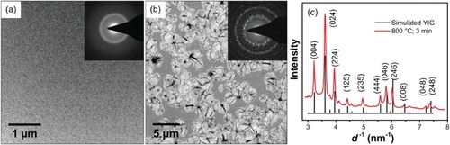
To benchmark typical microstructures and nanostructures, YIG films were deposited on TEM grids with SiO2 windows and imaged before and after standard annealing (RTA at 800°C for 3 min), shown in Figure (a,b, respectively). Figure (a) verifies that films were amorphous as-deposited. There were no structural features in the bright-field images, and the diffraction patterns were single diffuse rings due to a regularity in interatomic spacing typical in glassy structures [Citation34]. After annealing, Figure (b), the microstructure was similar to that typically seen in integrated YIG films by dark-field optical microscopy and scanning electron microscopy/electron backscatter diffraction [Citation24]. Micrometer-sized crystallites (1–2 µm) were observed in a seemingly amorphous matrix. These crystallites contained the desired garnet phase, but they only accounted for 80% of the sample area. However, because the YIG regions were highly crystalline, they were strongly diffracting and accounted for almost all of the intensity in the diffraction pattern, Figure (c). The angular intensity of the diffraction pattern was uniform, suggesting that the crystallites had no preferred in-plane texturing. The characteristic dark streaks throughout the crystallites arise from bend contours, a common diffraction-contrast feature in single-crystal films.
Figure 1. Bright-field TEM images and accompanying diffraction patterns of (a) as-deposited film and (b) RTA-annealed film (800°C, 3 min). Note: dark streaks in crystallites are a common diffraction-contrast feature in single crystals. (c) Radial integration of diffraction intensity for annealed film compared to simulated YIG data.
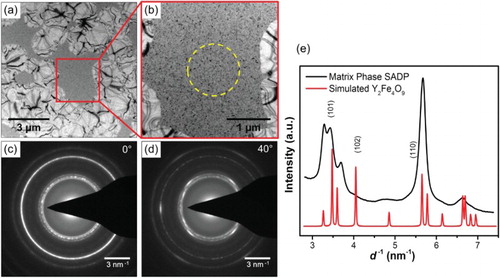
Further analysis of the matrix phase indicated that it was nanocrystalline (5–20 nm grains) rather than amorphous. Figure (a,b) shows bright-field images of this region with speckled contrast, which is indicative of multiple grains. Selected-area diffraction patterns (SADPs) of the matrix confirmed the presence of a crystalline phase. SADPs obtained at normal incidence consisted of sharp, continuous rings, signifying no in-plane texturing was present, Figure (c). However, tilting the specimen revealed a strong out-of-plane texturing in this nanocrystalline phase, as shown in Figure (d). Though the small grain size led to peak broadening, radial integration of the SADP, Figure (e), indicated that the matrix posed of out-of-plane textured Y2Fe4O9 nanocrystals. Due to the texturing, the relative peak intensities differ from those arising from a non-textured film, as can be seen by comparison to a simulated Y2Fe4O9 pattern. Importantly, the Y2Fe4O9 phase does not have desired ferromagnetic or magneto-optical properties, which explains the reduced performance in YIG films reported in the literature after standard RTA annealing [Citation16–17,Citation21–25,Citation33].
Figure 2. (a,b) Bright-field TEM images of the inter-YIG matrix phase present in films produced by standard anneals. The yellow circle in (b) shows the area from which SADPs were obtained. SADPs obtained at (c) 0°, showing no in-plane texturing and (d) 40°, suggesting out-of-plane texturing. (e) Radially integrated diffraction pattern compared to simulated Y2Fe4O9 with the three most prominent peaks indexed.
In situ TEM laser-induced crystallization
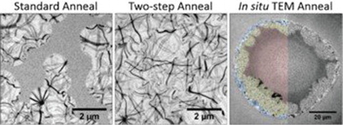
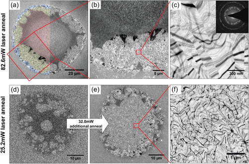
In order to study the amorphous-to-crystalline phase transition for YIG, in situ TEM laser-annealing studies were conducted on films deposited onto SiO2 on Si. These were similar to the as-deposited films shown in Figure (a). A relatively high average laser power (82.6 mW; 1 s; Gaussian shape) was used for in situ crystallization of the amorphous film. Further irradiation with this power produced no additional changes in the structure. Three regions with different crystallization behavior were identified, the formation of which is attributed to differences in temperature caused by the Gaussian energy profile of the laser similar to other in situ laser annealing studies, Figure (a) [Citation35–36]. The central dark region (red) was a nanocrystalline phase and was highly textured in-plane radially from the center of the spot due to the direction of thermal transport (see Supplemental Information). The second region (yellow) is shown more closely in Figure (b,c). The large grains in this region show bend contours due to the highly ordered crystalline structure, similar to the YIG crystallites in the RTA-annealed sample above. This region was pure YIG, as verified with SADP (inset of Figure (c)). The third region (blue), along the outer regions of the laser spot, was comprised of YIG crystallites that appeared to have seeded the growth in the second region. Using the known FWHM of the laser intensity, and assuming the second region reached the crystallization temperature of YIG (800°C), the third region was estimated to have reached 400°C (see Supplemental Information).
Figure 3. Bright-field images of YIG films crystallized with different laser powers. (a–c) Crystallization of YIG resulting from 82.6 mW average power, shown with relatively (a) low (b) medium and (c) high magnification. YIG nanocrystals near the edge of the spot appeared to seed larger crystals inside a ring. The inset in (c) shows an SADP of the highly crystalline YIG area. (d) Bright-field image of YIG film crystallized with 25.2 mW average power followed by (e) an additional 32.0 mW average power. The initial laser anneal at 25.2 mW appeared to create crystallites that seeded subsequent growth. (f) Magnified image of the film following the second additional anneal at 32 mW. See video of crystal growth in SI.
This growth behavior was unexpected, and it suggested that a low-temperature anneal could produce nuclei and/or seed crystallites, thereby enabling the rapid formation of YIG during subsequent high-temperature anneals. This low thermal budget concept for obtaining fully crystallized films is very appealing for eventual use in high-quality spintronics and photonics devices.
To study this idea further, a lower average power of 25.2 mW was used to form crystallites in as-deposited films, Figure (d). Further laser irradiation at this power did not produce any additional structural changes. However, increasing the average laser power to 32.0 mW caused these crystallites to grow with a crystallization front velocity of 280 nm/s, determined using time-resolved TEM, see Supplemental Information. Although the laser profile again yielded different behavior for the outer region of the beam, the entire center of the laser-annealed area was phase-pure YIG after this two-step anneal, Figure (e).
Novel two-step rapid thermal annealing
This study was brought full circle by applying the newly discovered means of nucleation and growth to a two-step RTA, which can be up-scaled for use with spintronics and photonics devices. YIG films (25 nm and 130 nm thick) were annealed by either standard RTA (800°C, 3 min), low-temperature RTA (400°C, 3 min), or two-step RTA (400°C, 3 min; 800°C, 3 min). The first RTA process has been the most common anneal for YIG [Citation17,Citation20,Citation24,Citation26–27,Citation29–30,Citation37] since its discovery [Citation30].
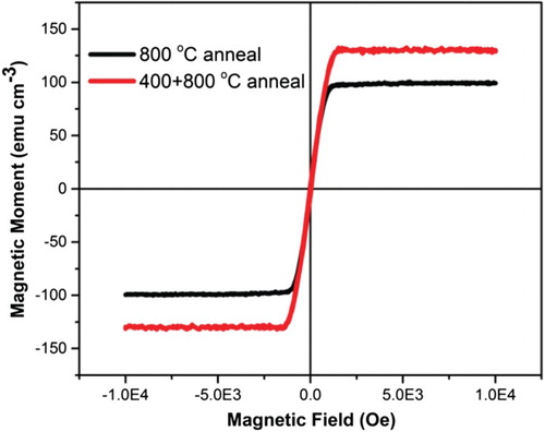
Magnetic hysteresis measurements (Figure ) were used to determine the extent of crystallization for YIG films that were annealed using both the standard RTA and the two-step RTA. The films produced by standard RTA had saturation magnetizations of 99.6 emu/cc, which is 27% lower than expected for pure YIG. Significantly, the YIG films annealed by the new two-step RTA had saturation magnetizations of 130.6 emu/cc, which is within experimental error (e.g.: film volume measurements) of reported values for YIG of 136.7 emu/cc [Citation38]. These results are in fair agreement with the difference in the garnet versus nanocrystalline areas found in the bright-field images shown in Figure .
Figure 4. Out-of-plane hysteresis loops of 130 nm thick YIG films annealed using standard RTA (800°C, 3 min) and the new two-step RTA (400°C, 3 min; 800°C, 3 min).
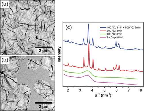
Additional TEM characterization supported the AGM result that the novel two-step RTA produced completely crystallized (phase-pure) YIG films, Figure (a), rather than the typical crystallites in a nanocrystalline matrix, which are produced by standard RTA, Figure (b). The diffraction patterns in Figure (c) underscore the challenge associated with determining the phase purity of YIG films from diffraction alone. Both patterns, corresponding to images on the left, have similar peak intensities and highly consistent peak locations. These patterns strongly suggest that standard, large-area Bragg–Brentano diffraction patterns (XRD) are not sufficient for reporting YIG crystallization of integrated devices because amorphous and ‘x-ray amorphous’ (nanocrystalline) phases will not appear in these patterns.
Figure 5. Bright-field TEM images of 25 nm YIG films (a) annealed at 400C° for 3 min and subsequently annealed at 800C° for 3 min and (b) annealed at only 800C° 3 min. (c) Radial integration of diffraction patterns for films annealed at various conditions. The diffraction patterns appear similar, but unlike standard anneals, the two-step anneal successfully produced phase-pure YIG.
In summary, the serendipitous discovery of a two-temperature anneal to aid the crystallization of YIG from thin films of amorphous Y–Fe–O led to the integration of phase-pure YIG films onto SiO2 on Si substrates. YIG films using standard single-temperature anneals are known to have poor performance in photonics even when standard diffraction patterns exhibit only garnet peaks. This has been attributed to incomplete crystallization [Citation20,Citation33]. Here, TEM analysis has shown that this matrix is actually a nanocrystalline, non-garnet phase accounting for over 20% of the sample. Due to the small grain size, this nanophase does not appear in the large-area diffraction pattern of YIG films, making it difficult to detect by standard characterization methods. In studying the crystallization of films using in situ laser annealing, seeding of garnet crystals was observed from crystallites produced at relatively low temperatures. Propagation of the crystallization front (280 nm/s) of garnet allowed this phase to consume the amorphous regions before the nanocrystalline phase could form. A commercially feasible two-step RTA technique (400°C, 3 min; 800°C, 3 min) was then proposed and successfully used for complete crystallization of phase-pure YIG films on SiO2 on Si. In addition to YIG, this innovation may be applicable to the Si-integration of other technologically important oxides, such as yttrium aluminum oxide (YAG) [Citation39], and it will most certainly play an important role in future device research and applications in nonreciprocal photonics, spintronics, and topological insulators.
Supplemantary_Material
Download MS Word (2.5 MB)Acknowledgements
Part of this work was performed at the Institute for Rock Magnetism (IRM) at the University of Minnesota.
Disclosure statement
No potential conflict of interest was reported by the authors.
Additional information
Funding
Related Research Data
References
- Vogel M, Chumak AV, Waller EH, et al. Optically reconfigurable magnetic materials. Nat Phys. 2015;11:487–491. doi: 10.1038/nphys3325
- Sun D, van Schooten KJ, Malissa H, et al. Inverse spin hall effect from pulsed spin current in organic semiconductors with tunable spin-orbit coupling. Nat Mater. 2016;15:863–869. doi: 10.1038/nmat4618
- Kirihara A, Uchida K-I, Kajiwara Y, et al. Spin-current-driven thermoelectric coating. Nat Mater. 2012;11:686–689. doi: 10.1038/nmat3360
- Jaworski C, Yang J, Mack S, et al. Observation of the spin-Seebeck effect in a ferromagnetic semiconductor. Nat Mater. 2010;9:898–903. doi: 10.1038/nmat2860
- An T, Vasyuchka V, Uchida K, et al. Unidirectional spin-wave heat conveyer. Nat Mater. 2013;12:549–553. doi: 10.1038/nmat3628
- Burrowes C, Heinrich B, Kardasz B, et al. Enhanced spin pumping at yttrium iron garnet/Au interfaces. Appl Phys Lett. 2012;100:092403. doi: 10.1063/1.3690918
- Heinrich B, Burrowes C, Montoya E, et al. Spin pumping at the magnetic insulator (YIG)/normal metal (Au) interfaces. Phys Rev Lett. 2011;107:066604. doi: 10.1103/PhysRevLett.107.066604
- Kajiwara Y, Harii K, Takahashi S, et al. Transmission of electrical signals by spin-wave interconversion in a magnetic insulator. Nature. 2010;464:262–266. doi: 10.1038/nature08876
- Kurebayashi H, Dzyapko O, Demidov VE, et al. Controlled enhancement of spin-current emission by three-magnon splitting. Nat Mater. 2011;10:660–664. doi: 10.1038/nmat3053
- Serga A, Chumak A, Hillebrands B. YIG magnonics. J Phys D: Appl Phys. 2010;43:264002. doi: 10.1088/0022-3727/43/26/264002
- Uchida K, Xiao J, Adachi H, et al. Spin Seebeck insulator. Nat Mater. 2010;9:894–897. doi: 10.1038/nmat2856
- Gruszecki P, Serebryannikov A, Śmigaj W, et al. Microwave excitation of spin wave beams in thin ferromagnetic films. Sci Rep. 2015.
- Lin W, Chen K, Zhang S, et al. Enhancement of thermally injected spin current through an antiferromagnetic insulator. Phys Rev Lett. 2016;116:186601. doi: 10.1103/PhysRevLett.116.186601
- Ishikawa A, Amemiya T, Shoji Y, et al. Optical and magnetic microstructures in YIG ferrite fabricated by femtosecond laser. J Laser Micro Nanoen. 2015;10:48–52. doi: 10.2961/jlmn.2015.01.0010
- Levy M, Osgood R, Hegde H, et al. Integrated optical isolators with sputter-deposited thin-film magnets. IEEE Photon Technol Lett. 1996;8:903–905. doi: 10.1109/68.502265
- Ristić M, Nowik I, Popović S, et al. Influence of synthesis procedure on the YIG formation. Mater Lett. 2003;57:2584–2590. doi: 10.1016/S0167-577X(02)01315-0
- Suzuki T. Magnetic and magneto-optic properties of rapid thermally crystallized garnet films. J Appl Phys. 1991;69:4756–4760. doi: 10.1063/1.348271
- Hahn C, de Loubens G, Klein O, et al. Comparative measurements of inverse spin hall effects and magnetoresistance in YIG/Pt and YIG/Ta. Phys Rev B: Condens Matter. 2013;87:174417. doi: 10.1103/PhysRevB.87.174417
- Onbasli MC, Beran L, Zahradník M, et al. Optical and magneto-optical behavior of cerium yttrium iron garnet thin films at wavelengths of 200–1770 nm. Sci Rep. 2016;6. doi: 10.1038/srep23640
- Bi L, Hu J, Jiang P, et al. On-chip optical isolation in monolithically integrated non-reciprocal optical resonators. Nature Photon. 2011;5:758–762. doi: 10.1038/nphoton.2011.270
- Ghosh S, Keyvavinia S, Van Roy W, et al. Ce: YIG/Silicon-on-Insulator waveguide optical isolator realized by adhesive bonding. Opt Express. 2012;20:1839–1848. doi: 10.1364/OE.20.001839
- Kahl S, Grishin AM. Enhanced Faraday rotation in all-garnet magneto-optical photonic crystal. Appl Phys Lett. 2004;84:1438–1440. doi: 10.1063/1.1651324
- Stadler BJ, Mizumoto T. Integrated magneto-optical materials and isolators: a review. IEEE Photon J. 2014;6:1–15. doi: 10.1109/JPHOT.2013.2293618
- Block AD, Dulal P, Stadler BJ, et al. Growth parameters of fully crystallized YIG, Bi: YIG, and Ce: YIG films with high faraday rotations. IEEE Photon J. 2014;6:1–8. doi: 10.1109/JPHOT.2013.2293610
- Fratello V, O’Bryan H, Brandle C. Search for high thermal expansion substrates for magneto-optic thick film garnets. J Cryst Growth. 1996;166:774–778. doi: 10.1016/0022-0248(95)00486-6
- Goto T, Onbaşlı MC, Ross C. Magneto-optical properties of cerium substituted yttrium iron garnet films with reduced thermal budget for monolithic photonic integrated circuits. Opt Express. 2012;20:28507–28517. doi: 10.1364/OE.20.028507
- Kumar N, Prasad S, Misra D, et al. The influence of substrate temperature and annealing on the properties of pulsed laser-deposited YIG films on fused quartz substrate. J Magn Magn Mater. 2008;320:2233–2236. doi: 10.1016/j.jmmm.2008.04.112
- Stadler BJ, Gopinath A. Magneto-optical garnet films made by reactive sputtering. IEEE Trans Magn. 2000;36:3957–3961. doi: 10.1109/20.914347
- Sun XY, Du Q, Goto T, et al. Single-step deposition of cerium-substituted yttrium iron garnet for monolithic on-chip optical isolation. ACS Photonics. 2015;2:856–863. doi: 10.1021/acsphotonics.5b00026
- Sung SY, Xiaoyuan Q, Stadler BJ. Integrating yttrium iron garnet onto nongarnet substrates with faster deposition rates and high reliability. Appl Phys Lett. 2005;87. Article number 121111. doi: 10.1063/1.2046733
- Uno T, Noge S. Growth of magneto-optic Ce: YIG thin films on amorphous silica substrates. J Eur Ceram Soc. 2001;21:1957–1960. doi: 10.1016/S0955-2219(01)00150-9
- Zhang Y, Xie J, Deng L, et al. Growth of phase pure yttrium iron garnet thin films on silicon: the effect of substrate and postdeposition annealing temperatures. IEEE Trans Magn. 2015;51:1–4.
- Holmes B, Hutchings D. Demonstration of quasi-phase-matched nonreciprocal polarization rotation in III-V semiconductor waveguides incorporating magneto-optic upper claddings. Appl Phys Lett. 2006;88:061116. doi: 10.1063/1.2172648
- Chukalkin YG, Shtirz V, Goshchitskii B. The structure and magnetism of amorphous Y3Fe5O12. Phys Status Solidi A. 1989;112:161–174. doi: 10.1002/pssa.2211120118
- Li T, Aji LB, Heo T, et al. Effect of medium range order on pulsed laser crystallization of amorphous germanium thin films. Appl Phys Lett. 2016;108:221906. doi: 10.1063/1.4953153
- Yoo B-K, Kwon O-H, Liu H, et al. Observing in space and time the ephemeral nucleation of liquid-to-crystal phase transitions. Nat Commun. 2015;6. Article no. 8639. doi: 10.1038/ncomms9639
- Bi L, Hu J, Kimerling L, et al. Fabrication and characterization of As2S3/Y3Fe5O12 and Y3Fe5O12/SOI strip-loaded waveguides for integrated optical isolator applications. Proceedings of the SPIE; 2010.
- Baek J, Ha S, Lim W, et al. Magnetostatic wave study of YIG films grown by the LPE method. Phys Status Solidi A. 2004;201:1806–1809. doi: 10.1002/pssa.200304554
- Stadler BJ, Oliveria M, Bouthillette LO. Alumina thin films as optical waveguides. J Am Ceram Soc. 1995;78:3336–3344. doi: 10.1111/j.1151-2916.1995.tb07974.x