
ABSTRACT
Herein, we spincast aqueous colloidal Ti2CTx (MXene) solutions into conductive, transparent films with figures of merit (FOM), that are as good as Ti3C2Tx or un-doped chemically vapor-deposited graphene. When normalized by the number of transition metal atoms, the FOM is the highest ever reported for a MXene film. At about 2.7 × 105 cm–1 the absorbance coefficient of Ti2CTx is quite comparable to that of Ti3C2Tx. Quantitative relationships between film properties—conductance and transparency—and colloidal solution concentration and spin speeds are developed providing a road map for future work.
GRAPHICAL ABSTRACT
IMPACT STATEMENT
In a first, we spincast aqueous colloidal Ti2CTx (MXene) solutions into conductive, transparent films with figures of merit—5—that are as good as Ti3C2Tx or un-doped CVD graphene.
KEYWORDS:
1. Introduction
Since the discovery of single-layered graphene and its remarkable properties, there has been a groundswell of interest in two-dimensional, 2D, materials [Citation1–11]. The desirable optical and electronic behavior resulting from reduced dimensionality is even further enriched by the opportunity for co-assembly of different 2D material-types to form novel heterojunctions [Citation12]. The classes of 2D materials known to date include graphene, transition metal dichalcogenides, metal oxides and double-metal hydroxides and MXenes, among others [Citation11]. Discovered in 2011 [Citation13,Citation14], MXenes are the youngest, and are so named because they are derived by selectively etching the A-element from Mn+1AXn (MAX) phases. The latter are layered transition metal carbides and nitrides where M is an early transition metal, A is an A-group element (mostly from groups 13 and 14) and X is C and/or N [Citation15]. The MAX structure comprises n + 1 near closed-packed layers of M (n = 1, 2 or 3) interleaved with hexagonal nets of the A-group elements. The X atoms occupy the octahedral sites between the M atoms. To create MXenes, a MAX phase powder is typically placed in HF-containing solutions that selectively etch the A layers and replace them by –O, –OH and –F terminations, forming multilayers. The proper designation of these 2D materials is thus Mn+1XnTx, where T stands for one of the aforementioned surface terminations [Citation16]. Multilayer MXene can be readily transformed into colloidal solutions using appropriate solvents, or by simply etching in a Li-ion containing solution [Citation17]. Currently, the number of different MXene chemistries is around 20—with more being discovered on a regular basis. However, to date, by far the most studied remains the first MXene discovered: Ti3C2Tx [Citation13]. This material has shown outstanding performance as an electrode material for supercapacitors and Li battery electrodes [Citation17–20], electromagnetic shielding [Citation21–23], among a slew of other applications [Citation24,Citation25].
In this work, Ti2CTx is explored as a transparent conductor. The latter can be broadly classified into two types: uniform and non-uniform [Citation26]. Ag-nanowires [Citation27] are a good example of non-uniform type. Examples of the former include, un-doped [Citation28] and doped graphene [Citation29,Citation30], MXenes [Citation8,Citation9,Citation31,Citation32] and the industry standard indium tin oxide, ITO. While the combination of transparency and conductivity of ITO is in general difficult to surpass, the high cost and limited supply of indium have energized efforts, especially in the 2D community, to find alternatives.
Films made of MXene colloidal solutions are typically quite conductive and hydrophilic [Citation14]. If the films are thin enough, they are also transparent [Citation8,Citation9,Citation31,Citation32]. For quantitative comparison of transparent conductors, we use a common figure of merit (FOM), defined as the ratio of the DC conductivity, σDC, to a quantity termed the ‘optical conductivity’, σOP, derived from the optical transmittance [Citation33].
To date all work in this area has focused on Ti3C2Tx [Citation8,Citation9,Citation31,Citation32]. Herein, we start to probe the importance of MXene chemistry on the optoelectronic properties of spincast films from aqueous colloidal solutions. Spincasting was the chosen method of producing our films because to date it has shown the largest FOM. Herein, we spincast Ti2CTx films and measured their transmittance and conductivity as a function of spin rotation and the solid content in the initial colloidal solutions. The relationships between film properties and processing conditions generated herein provide a map for future applications of this promising new 2D material.
2. Experimental details
To produce Ti2CTx colloidal solutions, we first etched Ti2AlC powders. The latter were produced by mixing Ti, Al and C elemental powders in a 2:1.1:1 molar ratio. The mixed powders were pre-compacted in a steel die using a load corresponding to a stress of 30 MPa. The compact was heated, in a tube furnace under flowing Ar, to 1400°C at a heating rate of 10°C/min and held at that temperature for 1 h before furnace cooling. The resulting lightly sintered compact was then milled into powders with a drill bit and passed through a‐180 mesh sieve. These powders were placed in a mixture containing 4 g of lithium fluoride, LiF (Alfa Aesar, 98%) and 40 ml of 11.7 M hydrochloric acid, HCl, solution for 24 h at 35°C.
The resulting suspension of multilayered Ti2CTx flakes was repeatedly washed with deionized water and centrifuged at a speed of 5000 rpm (3 min for each cycle). The resulting supernatant was then decanted and the process repeated until the supernatant reached a pH of ≈6. The resulting powder was mixed with about 20 ml of distilled water and sonicated for 1 h at room temperature under bubbling argon, Ar, gas and centrifuged for 30 min at a speed of 3500 rpm. Finally, the supernatant colloidal solution containing delaminated, mostly single 2D Ti2CTx flakes was stored in sealed bottles under, Ar, for further experiments.
For all the work carried out herein, the as-produced the starting concentration was 25 mg/ml. The solid content was determined by first vacuum filtering a given colloidal solution volume. The films were then stored for 2–3 days in a Drierite™ containing desiccator, after which they were weighed.
Films were spincast from the aforementioned colloidal solution and/or dilutions thereof with deionized water, DI. DI was added to the starting composition with a concentration of 25 mg/ml solution, to produce solutions with concentrations of 12.5, 8.33, 5, 2.5, 1.25, 0.5 and 0.25 mg/ml.
Typical films were spincast onto 2.5×2.5 cm2 glass substrates with spin speeds of 500, 800, 1000, 1500, 2000, 2500, 3000, 3500 or 4000 rpm for 30 s, followed by 2000 rpm for 5 s in all cases. Prior to spin coating, all substrates were cleaned with water and ethanol. The resultant films were stored in a dry N2 glove box (<1 ppm oxygen or moisture) overnight before characterization.
For comparison purposes, some films were made by dropping a few drops of the 25 mg/ml solution onto a glass slide and allowed to dry. These films were stored in air.
The spincast films were characterized by X-ray diffraction (Rigaku Smartlab) using Cu Kα1 radiation at a scan rate of 0.03°/step. The samples’ microstructures were imaged in a scanning electron microscope, SEM, (Zeiss Supra 50VP, Germany). The 2D Ti2CTx flakes were also imaged in a transmission electron microscope, TEM, (JEOL JEM-2100, Japan). To prepare the TEM samples, the colloidal solution was diluted with DI and a syringe was used to drop a drop on TEM grids. Prior to doing so, a piece of paper was placed under the grids to absorb any excess water and speed the drying process.
The films’ thicknesses were measured by a profilometer (NewView™ 8000, Zygo, CT). In a few cases, the SEM was also used to measure the thicknesses. When the two thickness measurements were compared least-squares analysis of the resulting straight line yielded a slope of 1.1 and an R2 value of 0.9. In other words, the profilometer results were in general agreement with the SEM ones.
The optical properties were determined using UV-vis-NIR spectrometry (Perkin-Elmer Lambda-950 UV/visible/NIR). To carry out the transmittance, τ, measurements the films were first deposited on glass substrates in ambient atmosphere. They were then stored in an N2 glove box for 24 h, taken out of the glove box, and their τ measured. In our previous work on Ti3C2Tx we showed that while exposure to the atmosphere affected the conductivities of the films, the effect on τ was minimal [Citation32].
The films were then placed back in the glove box. All electrical resistance measurements were carried out on the same films inside the glove box using a 4-point probe with a probe spacing of 2.3 mm (Keithley 2634B Sourcemeter) [Citation32]. Sheet resistance was measured 5 times at different locations across the film and averaged. It is worth noting here that τ was always measured before the electrical resistivities since the electrodes of the latter sometimes damaged the films.
3. Results and discussion
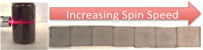
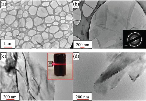
Pictures of a high (25 mg/ml) concentration colloidal solutions of Ti2CTx in water are shown in the inset of (c). The color is a deep purple when concentrated and indigo when diluted. When a laser is shined on the solution typical Tyndall scattering is observed (inset in (c)).
Figure 1. TEM images of Ti2CTx, (a) at low magnification showing a number of flakes; (b) at higher magnification. Inset shows SAD patterns of (11-20) with the electron beam parallel to <001>, (c, d) showing folding of flakes unto themselves and others. Inset in c shows the Tyndall effect in a colloidal solution.
These solutions and/or dilutions thereof with DI water were spincast into films. Two variables were explored: solid loading in the colloidal solution or concentration, c, and spincasting speed, ω. Starting with a solid content of 25 mg/ml, increased spincasting speeds—from 500 to 4000 rpm—resulted in more transparent films. Reducing the solid content—from 25 to 0.25 mg/ml—also resulted in more transparent films.
Typical TEM micrographs of Ti2CTx flakes are shown in . At low magnification, ((a)), the 2D flakes appear to have been delaminated with lateral dimensions of the order of 1 µm. (b) shows a higher magnification micrograph and a selected diffraction, SAD, pattern along (inset in Figure (b)) showing the polycrystalline nature of a collection of flakes. From the SAD patterns, it is clear that the flakes were initially individual flakes that had restacked in different orientations. The SAD also shows the hexagonal symmetry of the parent MAX phase, from which the a-lattice parameter is estimated to be about 0.3 nm. This value is in good agreement with the value of 0.306±0.001 nm reported for the parent MAX phase—Ti2AlC [Citation34].
In (a,b), the individual flakes appear to be quite flat. That does not imply they always are. Figure (c,d) shows TEM images of flakes that have folded on themselves. These TEM micrographs are noteworthy because the flakes appear to be of high quality, showing no signs of oxidation and/or other etching defects such as pores.
Typical XRD patterns (see Fig. S1 in supplementary materials) of spincast Ti2CTx films just after spincasting and after storage for a 100 d in a dry N2 glove box were typical MXene diffractograms in that the (000 l) peaks are downshifted in 2θ, while broadening considerably compared to those of Ti2AlC [Citation14]. The lack of any peaks belonging to the latter shows them to be largely free of un-etched starting material. As importantly no other oxide peaks can be seen. This is true even after storing in a dry N2 glove box for 100 d. The c-lattice parameters, c-LP, of these films—2.43 to 2.54 nm are considerably larger than the values obtained when the films are etched in 10% HF, where they are closer to 1.5 nm [Citation35]. This large difference can be attributed to the presence of multiple water layers between the flakes [Citation36]. Interestingly, this intercalated water is present even after storage in the dry N2 glove box for at least 100 d.
In order to explore the stability of the Ti2CTx films in air, the colloidal solution was dropcast and XRD patterns were measured immediately after deposition and again after storing for 100 d in air. When the XRD patterns (See Fig. S1 in supplementary material) were compared, they appeared to be identical suggesting that either the films are stable in air or if an oxide forms, it is amorphous. Interestingly, the c-LP in this case is about 0.5 nm larger than the spincast films. The increase suggests the presence of an extra water layer between the flakes as compared to the spincast films. Why this is the case is unclear at this time, but may be related to the fact that the dropcast films were in contact with water for a longer time as they were drying, and/or the fact that they were stored in air.
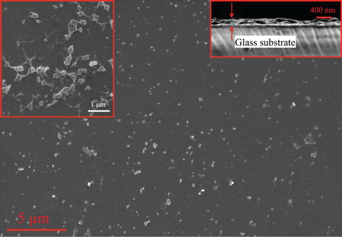
An SEM micrograph of a top view of a typical Ti2CTx film spincast on a glass slide is shown in . The top left inset shows the same at a higher magnification. The top right inset shows a typical cross-section of a ≈ 200 nm thick film. Not surprisingly, these films are quite reminiscent of our Ti3C2Tx spincast films in that for the most part they are quite smooth with what appears to be a small number of multilayer flakes sporadically sprinkled on the surface [Citation32]. At the magnification in , however, the film appears to be quite smooth.
Figure 2. Typical SEM image of top view of a Ti2CTx film spincast on a glass slide. Top left inset shows the same at a higher magnification. Top right inset shows a typical cross-section of a ≈ 200 nm thick film, determined from the distance between the two arrows.
(a,b) plots the film thicknesses, h, as a function of process variables. (a) plots the film thickness, h, on the reciprocal of the spinning speed, ω. A widely used formula in the literature on spincasting relating ω to h, is h = A ω−0.5, where A is a material—and solvent-specific constant. A least-squares fit to a plot of h versus ω−0.5 of our data gives h (nm) = 1280 ω−0.5, when the fit is forced to pass through the origin. As expected, higher spinning speeds, ω, resulted in thinner films ((a)). The effects of colloidal solution concentration, c, on thickness at spin speeds of 800 and 3500 rpm are shown in (b). If the least-squares fits of the results are forced through the origin, then at 3500 rpm, h (nm) ≈ 2.95c; at 800 rpm, h (nm) ≈ 6.1c where c is in mg/ml.
Figure 3. (a) Dependencies of film thicknesses, h, on, (a) 1/√ω for an initial concentration of 25 mg/ml. (b) Dependencies of film thicknesses, h, on concentration of colloidal solution, c, at spin speeds of 800 and 3500 rpm. (c) Optical transmittance, τ, over the visible spectrum of spincast Ti2CTx films as a function of c (top cluster) all spun at 3500 rpm and ω (lower cluster) all starting with a c = 25 mg/ml.
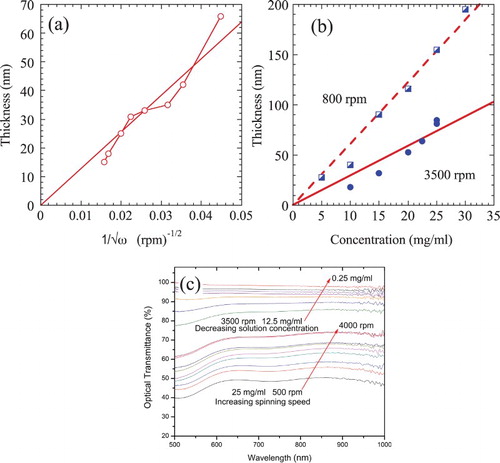
The dependencies of τ, at 550 nm, of the spincast films on ω and c are shown in (c). Not surprisingly, the faster rotation speeds and lower solid loadings result in thinner films that in turn are more transparent. Varying the spinning speed in the 500–4000 rpm range varies τ in the 43–65% range. The Ti2CTx films, spun at 3500 rpm can be increased from 62% to 99.9%, by varying c over the 25–0. 25 mg/ml range, respectively.
The dependencies of the sheet resistances, Rs in Ω/□ of the spincast films on h, ω and c are shown in (a, b), respectively. Here, again not surprisingly, thicker films exhibit lower sheet resistance (i.e. greater sheet conductance) than their thinner counterparts. Least-squares fits of the data points shown in the inset in (a) yields the following relationship: Rs ≈ 60.9 + 0.026 ω, with an R2 value >0.93. The relationship between Rs and film thickness, h, is shown in (a). Least-squares fits of the data points yield: 1/Rs (Ω/□)−1 = −0.01 + (6 ± 2)×10−4 h (nm), with an R2 value of >0.83. The results thus show a scatter. To gain more insight into the scatter, we used τ of the various films to calculate their thickness. When Rs was then plotted as a function of the τ-derived thicknesses calculated from Equation (1), the R2 values shot up from 0.83 to >0.97 (see Figure S2 in the Supplementary Information). From this we conclude that the scatter observed is related to our uncertainty in measuring the film thickness’ and or their non-uniformity. Fortuitously, the slopes of the corrected lines are ≈ 6.1 ± 0.4 × 10⁻⁴. In other words, using this correction does not change the slope, but simply narrows down the error bars considerably. Note this is not a circular argument since Rs and τ are independent measurements.
Figure 4. (a) Dependence of reciprocal of the sheet resistance, 1/Rs, of spincast Ti2CTx films on film thickness. Inset shows dependence on spin speed, ω, for a starting composition of 25 mg/ml and, (b) Dependence of Rs concentration, c, at a rotation speed of 3500 rpm. Note log–log nature of plot.
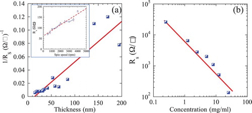
On the other hand, the relationship between the Rs and c (b) is given by: log Rs (Ω/□) ≈ 3.9–1.1 log c (mg/ml). In this case, the R2 value is >0.96.
The dependence of‐ln τ550 on film thickness, h, is shown in (a). A least-squares fit of these results, forced through the origin, yields the following relationship:
(1)
where α550—the absorption coefficient at 550 nm—is 2.65 × 105 cm−1. If the line is not forced through the origin, neglecting the intercept, α550 is 2.93×105 cm−1. Also plotted in (a) are our previous results on Ti3C2Tx [Citation32]. In that case, α550 is 2.5×105 cm−1. It is thus clear that within the experimental scatter, α550, for Ti3C2Tx and Ti2CTx, are comparable.
Figure 5. (a) Dependence of–ln τ550 on film thickness, h. Also plotted as a solid blue line are our previous results on Ti3C2Tx, [Citation32]. (b) Plot of left-hand side of Equation (2) vs. Zo/2Rs. Least-squares fits results in a slope of 0.2 with an R2 > 0.99.
![Figure 5. (a) Dependence of–ln τ550 on film thickness, h. Also plotted as a solid blue line are our previous results on Ti3C2Tx, [Citation32]. (b) Plot of left-hand side of Equation (2) vs. Zo/2Rs. Least-squares fits results in a slope of 0.2 with an R2 > 0.99.](/cms/asset/14ccf308-867a-4f46-94e6-a0626e46db79/tmrl_a_1296043_f0005_c.jpg)
In order to construct a dimensionless FOM to evaluate transparent conductors, it is common to use the fact that τ and Rs are linked by [Citation38]:
(2)
where σdc and σop are the DC and optical conductivities, respectively; Zo is the impedance of free space (377 Ω) [Citation38–40]. For a system that obeys this relation, a plot of the left-hand side vs. Zo/2Rs will result in a straight line, the slope of which is the dimensionless ratio σop/σdc. As observed ((b)), our data do fit this relationship, and the inverse of the slope thus determined provides our chosen FOM for transparent conductive films. In our case, the FOM is 5.
In this FOM is compared with other transparent conductive films. As noted previously [Citation32], our FOM is as good as un-doped, chemically vapor-deposited graphene films [Citation28] The relatively high FOM of these films is mostly because, at ≈ 1028 m−3, the density of charge carriers is high [Citation32,Citation44], leading to a high DC conductivity. Our films are not as good as doped CVD graphene [Citation29], ITO [Citation33] or Ag-nanowires [Citation27]. However, given that this is the first generation of such films, there is certainly room for improvement. As importantly the non-toxic, low cost and simplicity of producing our films are other advantages that cannot be easily dismissed.
Table 1. Comparison of the optoelectronic properties of solution processed MXenes fabricated here. Also listed for comparison are previous values for Ti3C2Tx films and other conductive transparent films.
Column 4 in compares the DC conductivities of the various films. The sheet conductivity of our 100 nm Ti2CTx films is 5250 S/cm which is slightly lower than that equally thick Ti3C2Tx films (6450 S/cm) [Citation32]. It is higher than that of other Ti3C2Tx films reported in previous MXene work [Citation8,Citation21], or reduced-GO [Citation41].
4. Summary and conclusions
Herein, aqueous colloidal solutions of the MXene, Ti2CTx, were spin-coated into transparent conductive films for the first time. Both the optical transmittances and DC conductivities were measured as a function of rotation speeds and concentration of Ti2CTx flakes in the initial colloidal solutions. At approximately 5, the FOM of our films is comparable to spincast Ti3C2Tx films.
With absorption coefficients α550 ≈ 2.7×105 cm−1, the absorptivities of the Ti2CTx and Ti3C2Tx films are comparable. However, this does not imply they are technologically equivalent. Per formula unit, the Ti2CTx films have one less atom of the relatively expensive element, Ti. Given the ease by which our films can be deposited from aqueous solutions, together with the fact that they are comprised of non-toxic relatively inexpensive abundant elements are advantages that bode well for their use in myriad applications where transparent and conductive films are required. Furthermore, it is reasonable to assume that, like in our previous work [Citation32], these films should retain their properties as they are flexed is another advantage.
Supplementary_Materials
Download MS Word (1 MB)Acknowledgements
XRD, SEM, and TEM investigations were performed at the Core Facilities at Drexel University. The authors thank S. Kota for taking the SEM micrographs.
Disclosure statement
No potential conflict of interest was reported by the authors.
Additional information
Funding
Related Research Data
References
- Bernardi M, Palummo M, Grossman JC. Extraordinary sunlight absorption and one nanometer thick photovoltaics using two-dimensional monolayer materials. Nano Lett. 2013;13:3664–3670. doi: 10.1021/nl401544y
- Bonaccorso F, Colombo L, Yu GH, et al. Graphene, related two-dimensional crystals, and hybrid systems for energy conversion and storage. Science. 2015;34:1–9.
- Eda G, Maier SA. Two-dimensional crystals: managing light for optoelectronics. ACS Nano. 2013;7:5660–5665. doi: 10.1021/nn403159y
- Gupta A, Sakthivel T, Seal S. Recent development in 2D materials beyond graphene. Prog Mater Sci. 2015;73:44–126. doi: 10.1016/j.pmatsci.2015.02.002
- Xia FN, Wang H, Xiao D, et al. Two-dimensional material nanophotonics. Nat Photonics. 2014;8:899–907. doi: 10.1038/nphoton.2014.271
- Yu WJ, Liu Y, Zhou HL, et al. Highly efficient gate-tunable photocurrent generation in vertical heterostructures of layered materials. Nat Nanotechnol. 2013;8:952–958. doi: 10.1038/nnano.2013.219
- Zhang CL, Yin HH, Han M, et al. Two-dimensional tin selenide nanostructures for flexible all-solid-state supercapacitors. ACS Nano. 2014;8:3761–3770. doi: 10.1021/nn5004315
- Mariano M, Mashtalir O, Antonio FQ, et al. Solution-processed titanium carbide MXene films examined as highly transparent conductors. Nanoscale. 2016;8:16371–16378-1-7. doi: 10.1039/C6NR03682A
- Hantanasirisakul K, Zhao MQ, Urbankowski P, et al. Fabrication of Ti3C2Tx MXene transparent thin films with tunable optoelectronic properties. Adv Electron Mater. 2016;2:1600050 1–7. doi: 10.1002/aelm.201600050
- Bhimanapati GR, Lin Z, Meunier V, et al. Recent advances in two-dimensional materials beyond graphene. ACS Nano. 2015;9:11509–11539. doi: 10.1021/acsnano.5b05556
- Zhang H. Ultrathin two-dimensional nanomaterials. ACS Nano. 2015;9:9451–9469. doi: 10.1021/acsnano.5b05040
- Novoselov KS, Mishchenko A, Carvalho A, et al. 2D materials and van der Waals heterostructures. Science. 2016;353:aac9439:1–11.
- Naguib M, Kurtoglu M, Presser V, et al. Two dimensional nanocrystals produced by exfoliation of Ti3AlC2. Advan Mater. 2011;23:4248–4253. doi: 10.1002/adma.201102306
- Naguib M, Mashtalir O, Carle J, et al. Two-dimensional transition metal carbides. ACS Nano. 2012;6:1322–1331. doi: 10.1021/nn204153h
- Barsoum MW. MAX phases: properties of machinable carbides and nitrides. Weinheim: Wiley VCH GmbH & Co.; 2013.
- Halim J, Cook KM, Naguib M, et al. X-ray photoelectron spectroscopy of two-dimensional transition metal carbides (MXenes). Appl Surf Sci. 2016;362:406–417. doi: 10.1016/j.apsusc.2015.11.089
- Ghidiu M, Lukatskaya MR, Zhao MQ, et al. Conductive two-dimensional titanium carbide ‘clay’ with high volumetric capacitance. Nature. 2014;516:78–81.
- Luo JM, Tao XY, Zhang J, et al. Sn4+ ion decorated highly conductive Ti3C2 MXene: promising lithium-ion anodes with enhanced volumetric capacity and cyclic performance. Acs Nano. 2016;10:2491–2499. doi: 10.1021/acsnano.5b07333
- Mashtalir O, Naguib M, Mochalin VN, et al. Intercalation and delamination of layered carbides and carbonitrides. Nat Commun. 2013;4:1716:1–7.
- Lukatskaya MR, Mashtalir O, Ren CE, et al. Cation intercalation and high volumetric capacitance of two-dimensional titanium carbide. Science. 2013;341:1502–1505. doi: 10.1126/science.1241488
- Shahzad F, Alhabeb M, Hatter CB, et al. Electromagnetic interference shielding with 2D transition metal carbides (MXenes). Science. 2016;353:1137–1140. doi: 10.1126/science.aag2421
- Han MK, Yin XW, Wu H, et al. Ti3C2 MXenes with modified surface for high-performance electromagnetic absorption and shielding in the X-band. ACS Appl Mater Interfaces. 2016;8:21011–21019. doi: 10.1021/acsami.6b06455
- Qing Y, Zhou W, Luo F, et al. Titanium carbide (MXene) nanosheets as promising microwave absorbers. Ceram Int. 2016;42:16412–16416. doi: 10.1016/j.ceramint.2016.07.150
- Ng VMH, Huang H, Zhou K, et al. Recent progress in layered transition metal carbides and/or nitrides (MXenes) and their composites: synthesis and applications. J Mater Chem A. 2017;5:3039–3068. doi: 10.1039/C6TA09817G
- Eklund P, Rosen J, Persson P. Layered ternary Mn+1AXn phases and their 2D derivative MXene: an overview from a thin-film perspective. J Phys D: Appl Phys. 2017;50:113001 1–14.
- Gao J, Kempa K, Giersig M, et al. Physics of transparent conductors. Adv Phys. 2016;65:553–617. doi: 10.1080/00018732.2016.1226804
- Hu L, Kim HS, Lee J-Y, et al. Scalable coating and properties of transparent, flexible, silver nanowire electrodes. ACS Nano. 2010;4:2955–2963. doi: 10.1021/nn1005232
- Wang X, Zhi L, Tsao N, et al. Transparent carbon films as electrodes in organic solar cells. Angew Chem. 2008;120:3032–3034. doi: 10.1002/ange.200704909
- Bae S, Kim H, Lee Y, et al. Roll-to-roll production of 30-inch graphene films for transparent electrodes. Nat Nanotech. 2010;5:574–578. doi: 10.1038/nnano.2010.132
- Bao W, Wan J, Han X, et al. Approaching the limits of transparency and conductivity in graphitic materials through lithium intercalation. Nat Commun. 2014;5:4224. 1–9.
- Halim J, Lukatskaya M, Cook KM, et al. Transparent conductive two-dimensional titanium carbide thin films. Chem Mater. 2014;26:2374–2381. doi: 10.1021/cm500641a
- Dillon AD, Ghidiu MJ, Krick AL, et al. Highly conductive optical quality solution-processed films of 2D titanium carbide. Adv Funct Mater. 2016;26:4162–4168. doi: 10.1002/adfm.201600357
- De S, Coleman JN. Are there fundamental limitations on the sheet resistance and transmittance of thin graphene films? ACS Nano. 2010;4:2713–2720. doi: 10.1021/nn100343f
- Radovic M, Ganguly A, Barsoum MW. Elastic properties and phonon conductivities of Ti3Al(C0.5,N0.5)2 and Ti2Al(C0.5,N0.5) solid solutions. J Mater Res. 2008;23:1517–1521. doi: 10.1557/JMR.2008.0200
- Naguib M, Come J, Dyatkin B, et al. MXene: a promising transition metal carbide anode for lithium-ion batteries. Electrochem Commun. 2012;16:61–64. doi: 10.1016/j.elecom.2012.01.002
- Ghidiu M, Halim J, Kota S, et al. Ion-exchange and cation solvation reactions in Ti3C2 MXene. Chem Mater. 2016;28:3507–3514. doi: 10.1021/acs.chemmater.6b01275
- De S, King PJ, Lyons PE, et al. Size effects and the problem with percolation in nanostructured transparent conductors. ACS Nano. 2010;4:7064–7072. doi: 10.1021/nn1025803
- Hu L, Hecht DS, Grüner G. Percolation in transparent and conducting carbon nanotube networks. Nano Lett. 2004;4:2513–2517. doi: 10.1021/nl048435y
- Dan B, Irvin GC, Pasquali M. Continuous and scalable fabrication of transparent conducting carbon nanotube films. ACS Nano. 2009;3:835–843. doi: 10.1021/nn8008307
- Becerril HA, Mao J, Liu Z, et al. Evaluation of solution-processed reduced graphene oxide films as transparent conductors. ACS Nano. 2008;2:463–470. doi: 10.1021/nn700375n
- Acerce M, Voiry D, Chhowalla M. Metallic 1T phase MoS2 nanosheets as supercapacitor electrode materials. Nat Nanotechnol. 2015;10:313–318. doi: 10.1038/nnano.2015.40
- Peng Q, Li S, Han B, et al. Colossal figure of merit in transparent-conducting metallic ribbon networks. Adv Funct Technol. 2016;1:1600095 1–4.
- Miranda A, Halim J, Barsoum MW, et al. Electronic properties of freestanding Ti3C2Tx MXene monolayers. App Phys Lett. 2016;108:033102 1–4.