
ABSTRACT
Heteroepitaxial films of GaO
were grown on c-plane sapphire (0001). The stable phase β-Ga
O
was grown using the metalorganic chemical vapor deposition technique, regardless of precursor flow rates, at temperatures between 500
C and 850
C. Metastable α- and ϵ-phases were grown when using the halide vapor phase epitaxy (HVPE) technique, at growth temperatures between 650
C and 850
C, both separately and in combination. XTEM revealed the better lattice-matched α-phase growing semi-coherently on the substrate, followed by ϵ-Ga
O
. The epitaxial relationship was determined to be [
] ϵ-Ga
O
[
] α-Ga
O
[
] α-Al
O
. SIMS revealed that epilayers forming the ϵ-phase contain higher concentrations of Cl introduced during HVPE growth.
GRAPHICAL ABSTRACT
IMPACT STATEMENT
This study demonstrates one of the first epitaxial growths of multiple polymorphs of GaO
on sapphire (0001) substrates, including its β-, α-, and ϵ-phases. Epitaxial relationship is confirmed through HRTEM.
KEYWORDS:
1. Introduction
The wide band gap material β-GaO
has attracted rapidly growing interest in the last decade due to its excellent potential for power [Citation1] and ultraviolet optoelectronic devices [Citation2] and its recent availability as single-crystal substrates [Citation3]. Roy et al. first synthesized and reported five polymorphs of Ga
O
, and designated them α-, β-, γ-, δ-, and ϵ-Ga
O
[Citation4]. δ-Ga
O
has since then been shown to be a nanocrystalline form of ϵ-Ga
O
[Citation5]. Of the four distinct polymorphs, most research has focused on the monoclinic β-phase, which is the only thermodynamically stable phase from room temperature to its melting point at ∼1800
C; all other polymorphs are metastable and have been reported to transform into the β-phase within the temperature range of 750–950
C [Citation6]. Single-crystal substrates of β-Ga
O
are grown by a variety of melt-based methods, including floating-zone (FZ) [Citation7–10], edge-defined film-fed growth (EFG) [Citation11], and Czochralski (CZ) [Citation12,Citation13] methods. Epitaxial films of β-Ga
O
have been grown using various vapor phase techniques, including metalorganic chemical vapor deposition (MOCVD) [Citation14], molecular beam epitaxy (MBE) [Citation1,Citation15–19], pulsed-laser deposition (PLD) [Citation20], halide vapor phase epitaxy (HVPE) [Citation21], and MIST epitaxy [Citation22].
However, increasing interest in the other GaO
phases has arisen in recent years, particularly the metastable rhombohedral α- and hexagonal ϵ-Ga
O
phases, both of which have been observed to grow epitaxially on oriented substrates. The α- and ϵ-phases are of particular interest because of their higher symmetry and simpler epitaxial relationships with c-plane sapphire. Moreover, given their similar structures to other wide bandgap materials such as ZnO and AlN, it should be possible to produce functional heterostructures or tunable bandgaps through alloying. A summary of the crystal parameters of α-, β-, and ϵ-Ga
O
are provided in Table ; for more detailed descriptions of the crystal structures, the reader is referred to [Citation5,Citation23]. On c-plane sapphire, typical orientations of the α-, β-, and ϵ-phases are (0001),
, and (0001), respectively. These orientations correspond to lattice mismatches of 4.7%, 6.12%, and 5.6% to c-plane sapphire, respectively. α-Ga
O
is the best lattice-matched polymorph and has the same corundum structure of sapphire.
Table 1. Crystal parameters for α-Ga O, β-GaO, and ϵ-GaO [Citation5,Citation23,Citation24].
Reports of successful epitaxial growths of the meta-stable α- and ϵ-GaO
phases have recently emerged. Table summarizes the growth methods, growth conditions, and resulting phase(s) described in these reports. With the exception of plasma-assisted MBE [Citation16] growth of β-Ga
O
containing α-Ga
O
inclusions, which was conducted in the range of 500–1000
C, all reported films containing only α- and ϵ-Ga
O
were grown at temperatures of ≤800
C. By comparison, typical growth temperatures of β-Ga
O
epitaxial layers by MOCVD are ∼1100
C, although early MOCVD growth of β-Ga
O
was reported at a growth temperature of 500–600
C [Citation14]. The resulting epitaxial polymorph appears to be determined by a number of conditions, including growth temperature, growth rate, substrate, and source gases; i.e. the stable β-polymorph is favored at higher growth temperatures but can also form at lower growth temperatures, particularly on β-Ga
O
substrates or at slow growth rates.
Table 2. Summary of epitaxial growths of α- and ϵ-GaO reported in the literature.
In the present study, the growth of α-, β- and ϵ-GaO
epitaxial films on c-plane sapphire (001) substrates were investigated using different growth conditions, including choice of precursors, flow rates and growth temperatures. Two different growth methods were used: metalorganic chemical vapor deposition (MOCVD) and HVPE. HVPE produced a significantly higher growth rate than MOCVD and is therefore advantageous for growth of the very thick films needed in high voltage power devices. Results from X-ray diffraction (XRD), scanning electron microscopy (SEM), high-resolution transmission electron microscopy (TEM) and secondary ion mass spectrometry (SIMS) are presented in the following sections and discussed in terms of the relationships between the growth conditions and the properties of the films.
2. Method
All samples discussed in this paper were grown in an in-house vertical vapor phase epitaxy reactor at Structured Materials Industries, Inc. (SMI). The reactor consists of a 16-inch diameter stainless steel chamber and a single rotating disc reactor with a 13-inch platter. Gas flows from a showerhead at the top of the chamber. All substrates used in this work were single-side chemo-mechanically polished, 2-inch diameter, c-plane (001) unintentionally doped (UID) sapphire (AlO
) wafers obtained commercially.
For the MOCVD growth runs, the chamber pressure was held at 45 Torr and the temperature was varied from 500C to 850
C. We established a baseline temperature at 650
C. These conditions were found by SMI in previous studies to maximize growth rate [Citation33]. Trimethylgallium (TMGa) and O
were used as precursors, with Ar used as the carrier gas. Typical growth rates were ∼10 nm/min.
For the HVPE growth runs, two different precursor processes were used. First, 15% HCl in Ar flowing at rates between 138 and 300 sccm over Ga metal was used to form GaCl at 600C. The substrate temperature was varied between 650
C and 800
C and chamber pressure was kept at 550 Torr. In the second process, Ar carrier gas flowed at 200 sccm into the bubbler held at 700 Torr and 80
C to yield a nominal GaCl
flow of ∼3.3 sccm. The substrate temperature and chamber pressure were kept at 600
C and 550 Torr, respectively. O
was used as the oxygen source in both process routes.
SEM images were acquired using an FEI Quanta 600 FEG scanning electron microscope at 15 keV. Secondary electron images were collected using an Everhardt Thornley secondary electron detector. XRD scans were conducted using a Panalytical X'pert Pro MPD X-ray diffractometer with a Cu X-ray source. Transmission electron microscopy (TEM) was conducted with an FEI Titan G2 80–300 operating at 300 kV. Images were taken with a
slow-scan CCD camera. SIMS was performed by EAG Analytical on a Physical Electronics ADEPT 1010, Cs was used as the primary beam at 5 keV and the negative ions were collected. Results were calibrated with reference to a standard made by ion implantation of Cl into a single-crystal Ga
O
substrate. Anneals of the implanted samples were performed at 700–1000
C for 1 h in a quartz tube in a resistively heated furnace under an Ar ambient.
3. Results
In concurrence with standard reports of GaO
epitaxy, all films grown in this research by MOCVD were observed to be β-Ga
O
. Figure (a) shows the XRD spectrum of a representative β-Ga
O
film grown at 650
C, with peaks for the set of
planes of β-Ga
O
at
, 38.420
, 59.184
and 82.375
, corresponding to the (
01), (
02), (
03) and (
04) reflections. The peak at
is attributed to the (0006) reflection of the sapphire substrate and is common for all the spectra in this figure. Schewski et al. reported the presence of a pseudomorphic layer of α-phase at the Ga
O
/sapphire interface [Citation25]. A shoulder is indeed observed at
, which is the location of the α-Ga
O
(0006) peak. However, this shoulder is observed even on a bare sapphire substrate, and our cross-sectional TEM of a β-Ga
O
/sapphire sample did not reveal the presence of an interfacial layer in the local regions observed, as shown in Figure (a). The epitaxial relationship was determined to be (
01) β-Ga
O
(0001) α-Al
O
, which agrees with previous reports [Citation16].
Figure 1. XRD of (a) β, (b) α, and (c) ϵ-phases. Growth conditions are shown in Table .
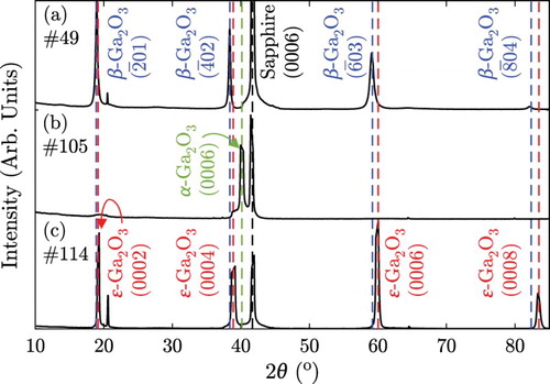
Table 3. Growth conditions for β, α, and ϵ-GaO films corresponding to the XRD patterns shown in Figure (a)–(c), respectively.
In contrast, the films grown by HVPE were found to consist of α- and/or ϵ-GaO
. Figure (b,c) shows the XRD spectra of two samples (#105 and #114) also grown at 650
C containing α- and ϵ-Ga
O
as the respective dominant phases. For sample #105 (Figure (b)), the XRD peak at 40.15
corresponds to the (0006) reflection of α-Ga
O
, while the bump at 19.16
and shoulder at 38.88
suggest that this sample may also contain minor amounts of ϵ-Ga
O
. For sample #114, peaks for the ϵ-Ga
O
set of planes were observed at 19.16
, 38.88
, 60.06
, and 83.50
, corresponding to the (0002), (0004), (0006), and (0008) reflections, respectively. The XRD results shown in Figure are similar to results we reported previously for samples grown under slightly different growth conditions [Citation34].
In order to understand the growth conditions giving rise to the metastable phases during HVPE, a series of HVPE growth runs with different carrier gas flow rates was investigated. GaCl was used as the Ga precursor and was kept at a constant flow rate of 200 sccm, and at temperature and pressure of 80
C and 700 Torr, respectively. Chamber pressure and growth temperature were 550 Torr and 650
C, respectively. All growth runs were for 1 h.
SEM images of these HVPE films (growth runs #86–#89) are presented in Figure (a)–(d), respectively. Distinctive hexagonal islands were observed on the surfaces of films #86 and #87, as shown in Figure (a,b), respectively. This observation is consistent with a reported island growth mechanism for ϵ-GaO
[Citation30]. Comparison of the SEM images in Figure (b,c) shows that the islands grew to a maximum size of ∼200 nm prior to the onset of coalescence. The surface coverage increases from left to right in general correspondence with a decrease in the O
flow rate and increase in the Ar flow rate. For sample #89 (Figure (d)), the film achieved complete coverage; according to a spectral reflectometry measurement, the thickness of the film was ∼300 nm. Accurate thickness measurements of the other films were not obtained due to their non-uniform coverage.
Figure 2. SEM images showing a series of heteroepitaxial GaO
films having respective sample #s 86–89 and grown by HVPE on c-plane sapphire. The Ar and O
flow rates are indicated. The inset of (b) shows a magnified image of the hexagonal islands achieved under these particular conditions; they were also present in the film shown in (a). (e) XRD of samples shown in (a)–(d), respectively.
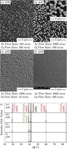
XRD θ-2θ scans shown in Figure (e) indicate that HVPE film #'s 86–89 consist of varying amounts of α- and ϵ-phases. The relative ϵ-to-α-phase peak intensity ratio increased with increasing Ar flow rate, or with increasing film coverage (from left to right, in Figure (a–d)).
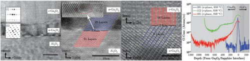
An increase in the amount of ϵ-GaO
relative to α-Ga
O
with increasing thickness can be understood by observing the film/substrate interface in cross-section. A cross-section HRTEM image of sample #89 along the [
] zone axis of sapphire is shown in Figure (b). An ∼10nm thick interfacial layer on the sapphire substrate was identified as α-Ga
O
. The remainder of the film above the α-Ga
O
layer was identified as ϵ-Ga
O
. Based on the data shown in Figures and , it is possible that the film growth follows a Stranski-Krastanov-like growth mode, beginning with a semi-coherent layer of α-Ga
O
on the sapphire substrate, followed by island growth of ϵ-Ga
O
. Further studies are needed to verify the growth mode.
Figure 3. (a) Cross-section TEM of β-GaO
epitaxial layer grown by MOCVD on sapphire (0001) at 650
C. The epitaxial relationship is [
01] β-Ga
O
[0001] α-Al
O
. (b) Cross-section HRTEM of Ga
O
on c-plane sapphire along the Al
O
[
] zone axis (sample #89). An ∼10nm thick interfacial layer of α-Ga
O
grew directly on the substrate, followed by a thicker layer of ϵ-Ga
O
. Insets shows selected area diffraction corresponding to (i) ϵ-Ga
O
[
] and (ii) α-Ga
O
[
]. The epitaxial relationship was found to be [
] ϵ-Ga
O
[
] α-Ga
O
[
] α-Al
O
. (c) Cross-section HRTEM of α-Ga
O
on c-plane sapphire along the α-Al
O
[
] zone axis. Inset is magnified image of misfit dislocation. (d) Cross-section HRTEM of ϵ-Ga
O
on α-Ga
O
along the α-Ga
O
[
] zone axis.
![Figure 3. (a) Cross-section TEM of β-GaO epitaxial layer grown by MOCVD on sapphire (0001) at 650C. The epitaxial relationship is [01] β-GaO [0001] α-AlO. (b) Cross-section HRTEM of GaO on c-plane sapphire along the AlO [] zone axis (sample #89). An ∼10nm thick interfacial layer of α-GaO grew directly on the substrate, followed by a thicker layer of ϵ-GaO. Insets shows selected area diffraction corresponding to (i) ϵ-GaO [] and (ii) α-GaO []. The epitaxial relationship was found to be [] ϵ-GaO [] α-GaO [] α-AlO. (c) Cross-section HRTEM of α-GaO on c-plane sapphire along the α-AlO [] zone axis. Inset is magnified image of misfit dislocation. (d) Cross-section HRTEM of ϵ-GaO on α-GaO along the α-GaO [] zone axis.](/cms/asset/7665d23f-ea11-488c-8adc-fcdf23bc53ee/tmrl_a_1443978_f0003_c.jpg)
The selected area diffraction pattern of the interfacial layer matches well with the [] zone axis of α-Ga
O
. Furthermore, a closer examination of the sapphire/α-Ga
O
interface in Figure (c) reveals a lattice offset that corresponds to the lattice mismatch between α-Ga
O
and c-plane sapphire. This shows that the α-epilayer grew semi-coherently on the sapphire substrate. Since the (
) lattice spacings of α-Ga
O
and sapphire projected along the [
] are 4.3 and 4.1 Å, respectively, in a relaxed film every 20 layers of α-Ga
O
should correspond to 21 layers of sapphire. A misfit dislocation is generated every 8.6 nm.
As shown in Figure (b), after ∼10nm the α-phase transitioned to the ϵ-phase. Twinning is observed in the ϵ-phase due to the hexagonal sixfold symmetry of ϵ-GaO
and its island nucleation growth mode. The selected area diffraction pattern for one grain of the top layer matches closely with the [
] zone axis of ϵ-Ga
O
. This shows that ϵ-Ga
O
[
] is oriented parallel to α-Ga
O
[
] as shown in Figure (d), which corresponds to a rotation of 30
C respective to each other. The other grains are 60
C rotations in the xy-plane. Since the lattice spacing in the [
] directions of ϵ-Ga
O
is 1.45 Å, 18 layers of ϵ-Ga
O
is about 2.6 nm; this agrees with our TEM observations.
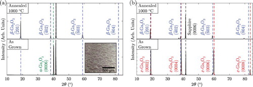
Since α- and ϵ-GaO
are metastable phases, we annealed them to determine at what temperature they would transform to β-Ga
O
. The results of XRD characterization are shown in Figure . Figure (a) shows that α-Ga
O
transformed into β-Ga
O
after annealing at 700
C in air for 1 h. Crystalline facets were observed and were visible to the naked eye (Figure (inset)). ϵ-Ga
O
was also annealed in air for 1 h between 700
C and 1000
C in 100
C increments. The transformation from ϵ-Ga
O
to β-Ga
O
was detected only after annealing at 1000
C, as shown in Figure (b). There were no visible changes in the surface microstructure as a function of annealing temperature for the ϵ-to-β-Ga
O
samples. In comparison, a previous study [Citation35] reported complete transformation from ϵ-to-β-Ga
O
after a 3-hr anneal at 900
C, whereas analysis by differential scanning calorimetry indicated the transformation actually begins somewhere between 700
C and 800
C.
Figure 4. (a) XRD of α-GaO
grown on c-plane sapphire before and after annealing at 700
C for 1 h. Insert shows an optical image of the surface microstructure of the β-Ga
O
that transformed from the α-Ga
O
after annealing at 700
C for 1 h. (b) XRD of ϵ-Ga
O
grown on c-plane sapphire before and after annealing at 1000
C for 1 h.
4. Discussion
Films grown via MOCVD on (001) sapphire substrates in the temperature range of 500–850C consistently yielded the stable β-Ga
O
phase. In contrast, deposition using HVPE within approximately the same temperature range of 650–850
C consistently resulted in the growth of metastable α- and ϵ-Ga
O
phases. The fact that both the α- and ϵ-Ga
O
are better lattice matched with the substrate surface crystallography alone does not explain why these phases were not observed when grown using the MOCVD technique. One reason for the non-equilibrium growth during HVPE that is common for all these samples is the significantly faster growth rate, that did not allow the adatoms time to rearrange to form the thermodynamically stable β-phase. I.e. the diffusing adatoms initially bonded to the oxygen and aluminum sites of the (0001) surface, mimicked the surface crystallography (α-Ga
O
also possesses the corundum structure) and were unable to undergo rearrangement to the β-Ga
O
phase before the next layer of adatoms had deposited on the surface. Each layer of α-Ga
O
was constrained or buried by the rapidly depositing subsequent layers. Moreover, the period after the cessation of growth was too brief and the cooling rate too fast to allow the transformation to the β-Ga
O
that was achieved during longer term annealing at 700
C, the center of the deposition range.
A second reason for the sequential occurrence of both the α- and ϵ-GaO
phases in the HVPE grown samples is believed to be associated with the presence of Cl, as revealed in SIMS investigations of three additional samples grown under the conditions noted in Table and resulting from incorporation from GaCl/GaCl
used during growth. The Cl detection limit on the tool is
atoms/cc. The depth profiles acquired from these studies are shown in Figure (a)–(c). A comparison plot of the Cl concentrations in the three films in Figure (d) and the associated data presented in Table reveal the average Cl concentration in samples #112 and #165 to be 1–2 orders of magnitude higher than in sample #105. All profiles show a very high Cl concentration at the Ga
O
/Al
O
interface that ranges from
atoms/cc (#165) to
atoms/cc (#105 and #112). The presence of Cl at the outset of growth would result in the formation of very stable Al–Cl bonds at the Al
O
(0001) surface having a bond dissociation energy,
kJ/mole, and changes in both the surface energy of the sapphire and the interfacial energy between the two oxides. The overriding factor (rapid growth rate, similarity in crystal structure and favorable lattice matching, high concentrations of Cl) that controls the formation of the α-Ga
O
cannot be determined unequivocally; however, it surmounts all other phenomena that would initiate the formation of either the β or the ϵ phases.
Figure 5. Cl− concentration in atoms/cc and Ga, Al and O concentration in arbitrary units, measured by SIMS for samples (a) #105, (b) #112, and (c) #165, respectively. (d) Cl− concentration in three samples measured by SIMS. Sample #105 shows α-phase and was grown at 650C, sample #112 shows ϵ-phase and was grown at 650
C. Sample #165 shows ϵ-phase and was grown at 850
C.
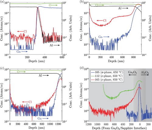
Table 4. Growth conditions for three growth runs of heteroepitaxial GaO on c-plane sapphire using HVPE.
However, the presence of Cl apparently affects the onset of formation and continued growth of the ϵ phase atop the α phase. The SIMS profile and the phase result in Table for sample #105 shows that the Cl is solely concentrated at the GaO
/Al
O
interface and that α-Ga
O
is the only deposited phase, respectively. By contrast, the analogous profiles and phase results for samples #112 and #165 reveal the presence of Cl either throughout the entire film (#112) or primarily contained in approximately half the film (#165) and the formation of the ϵ-Ga
O
phase, respectively. The reason for the latter set of results may be associated with incorporation of the Cl to relieve stress in the growing film. Consider that Cl− has an ionic radius of 167 pm, compared to 126 pm for O2−. If Cl substitutes for O in the crystal lattice, it would introduce compressive stresses in the lattice. Note that the ϵ-phase has a larger lattice spacing than the α-phase and should therefore accommodate Cl impurities more easily. Further investigations are necessary to confirm or provide other explanations for these results.
5. Summary
Growth of the stable phase β-GaO
was achieved on (0001) sapphire substrates using MOCVD within the temperature range of 650–850
C. The metastable phases α- and ϵ-Ga
O
were observed when grown at the same temperature range using HVPE. The growth of these latter phases is likely due to a combination of high growth rates and low growth temperature. Although Cl was detected in the HVPE grown films – and was highest in the ϵ-Ga
O
layers – the possible role of Cl in the growth mechanism requires further investigation.
Acknowledgements
The authors would like to acknowledge Mr Noel T. Nuhrer from the Materials Characterization Facility at the Carnegie Mellon University for his extensive help with transmission electron microscopy, and Raveena Gangireddy for help with sample preparation.
Disclosure statement
No potential conflict of interest was reported by the authors.
ORCID
Additional information
Funding
References
- Higashiwaki M, Sasaki K, Kuramata A, et al. Development of gallium oxide power devices. Phys Status Solidi A. 2014;211(1):21–26. doi: 10.1002/pssa.201330197
- Oshima T, Okuno T, Arai N, et al. Vertical solar-blind deep-ultraviolet Schottky photodetectors based on β-GaO substrates. Appl Phys Express. 2008;1(1):011202. doi: 10.1143/APEX.1.011202
- Tamura Corporation. Single-crystal gallium oxide substrates; 2017 [cited 2017 Aug 28]. Available from: http://www.tamura-ss.co.jp/en/products/gao/index.html.
- Roy R, Hill VG, Osborn EF. Polymorphism of GaO and the system GaO-HO. J. Am. Chem. Soc.. 1952;74(3):719–722. doi: 10.1021/ja01123a039
- Playford HY, Hannon AC, Barney ER, et al. Structures of uncharacterised polymorphs of gallium oxide from total neutron diffraction. Chem Eur J. 2013;19(8):2803–2813. doi: 10.1002/chem.201203359
- Lee SD, Ito Y, Kaneko K, et al. Enhanced thermal stability of alpha gallium oxide films supported by aluminum doping. Jpn J Appl Phys. 2015;54(3):030301.
- Ueda N, Hosono H, Waseda R, et al. Synthesis and control of conductivity of ultraviolet transmitting β-GaO single crystals. Appl Phys Lett. 1997;70:3561–3563. doi: 10.1063/1.119233
- Víllora EG, Shimamura K, Yoshikawa Y, et al. Large-size β-GaO single crystals and wafers. J Cryst Growth. 2004;270(3):420–426. doi: 10.1016/j.jcrysgro.2004.06.027
- Suzuki N, Ohira S, Tanaka M, et al. Fabrication and characterization of transparent conductive Sn-doped β-GaO single crystal. Phys Status Solidi C. 2007;4(7):2310–2313. doi: 10.1002/pssc.200674884
- Víllora EG, Shimamura K, Yoshikawa Y, et al. Electrical conductivity and carrier concentration control in β-GaO by Si doping. Appl Phys Lett. 2008;92:202120.
- Aida H, Nishiguchi K, Takeda H, et al. Growth of β-GaO single crystals by the edge-defined, film fed growth method. Jpn J Appl Phys. 2008;47(11R):8506. doi: 10.1143/JJAP.47.8506
- Tomm Y, Ko J, Yoshikawa A, et al. Floating zone growth of β-GaO: a new window material for optoelectronic device applications. Sol Energy Mater Sol Cells. 2001;66(1):369–374. doi: 10.1016/S0927-0248(00)00196-3
- Galazka Z, Uecker R, Irmscher K, et al. Czochralski growth and characterization of β-GaO single crystals. Cryst Res Technol. 2010;45(12):1229–1236. doi: 10.1002/crat.201000341
- Kim HW, Kim NH. Growth of gallium oxide thin films on silicon by the metal organic chemical vapor deposition method. Mater Sci Eng B. 2004;110(1):34–37. doi: 10.1016/j.mseb.2004.01.012
- Víllora EG, Shimamura K, Kitamura K, et al. Epitaxial relationship between wurtzite GaN and β-GaO. Appl Phys Lett. 2007;90(23):234102. doi: 10.1063/1.2745645
- Oshima T, Okuno T, Fujita S. GaO thin film growth on c-plane sapphire substrates by molecular beam epitaxy for deep-ultraviolet photodetectors. Jpn J Appl Phys. 2007;46(11):7217–7220. doi: 10.1143/JJAP.46.7217
- Higashiwaki M, Sasaki K, Kuramata A, et al. Gallium oxide (GaO) metal-semiconductor field-effect transistors on single-crystal β-GaO (010) substrates. Appl Phys Lett. 2012;100(1):013504. doi: 10.1063/1.3674287
- Higashiwaki M, Sasaki K, Kamimura T, et al. Depletion-mode GaO metal-oxide-semiconductor field-effect transistors on β-GaO (010) substrates and temperature dependence of their device characteristics. Appl Phys Lett. 2013;103(12):123511. doi: 10.1063/1.4821858
- Sasaki K, Higashiwaki M, Kuramata A, et al. MBE grown β-GaO and its power device applications. J Cryst Growth. 2013;378:591–595. doi: 10.1016/j.jcrysgro.2013.02.015
- Orita M, Hiramatsu H, Ohta H, et al. Preparation of highly conductive, deep ultraviolet transparent β-GaO thin film at low deposition temperatures. Thin Solid Films. 2002;411(1):134–139. doi: 10.1016/S0040-6090(02)00202-X
- Murakami H, Nomura K, Goto K, et al. Homoepitaxial growth of β-GaO layers by halide vapor phase epitaxy. Appl Phys Express. 2014;8(1):015503.
- Oshima Y, Víllora EG, Shimamura K. Quasi-heteroepitaxial growth of β-GaO on off-angled sapphire (0001) substrates by halide vapor phase epitaxy. J Cryst Growth. 2015;410:53–58. doi: 10.1016/j.jcrysgro.2014.10.038
- Stepanov S, Nicolaev V, Bougrov V, et al. Gallium oxide: properties and applications – a review. Rev Adv Mater Sci. 2016;44:63–86.
- Åhman J, Svensson G, Albertsson J. A reinvestigation of β-gallium oxide. Acta Crystallogr C. 1996;52(6):1336–1338. doi: 10.1107/S0108270195016404
- Schewski R, Wagner G, Baldini M, et al. Epitaxial stabilization of pseudomorphic α-GaO on sapphire (0001). Appl Phys Express. 2014;8(1):011101.
- Akazawa H. Formation of various phases of gallium oxide films depending on substrate planes and deposition gases. Vacuum. 2016;123:8–16. doi: 10.1016/j.vacuum.2015.10.009
- Shinohara D, Fujita S. Heteroepitaxy of corundum-structured α-GaO thin films on α-AlO substrates by ultrasonic mist chemical vapor deposition. Jpn J Appl Phys. 2008;47(9R):7311. doi: 10.1143/JJAP.47.7311
- Oshima Y, Víllora EG, Shimamura K. Halide vapor phase epitaxy of twin-free α-GaO on sapphire (0001) substrates. Appl Phys Express. 2015;8(5):055501. doi: 10.7567/APEX.8.055501
- Mezzadri F, Calestani G, Boschi F, et al. Crystal structure and ferroelectric properties of ϵ-GaO films grown on (0001)-sapphire. Inorg Chem. 2016;55(22):12079–12084. doi: 10.1021/acs.inorgchem.6b02244
- Boschi F, Bosi M, Berzina T, et al. Hetero-epitaxy of ϵ-GaO layers by MOCVD and ALD. J Cryst Growth. 2016;443:25–30. doi: 10.1016/j.jcrysgro.2016.03.013
- Oshima Y, Víllora EG, Matsushita Y, et al. Epitaxial growth of phase-pure ϵ-GaO by halide vapor phase epitaxy. J Appl Phys. 2015;118(8):085301. doi: 10.1063/1.4929417
- Nishinaka H, Tahara D, Yoshimoto M. Heteroepitaxial growth of ϵ-GaO thin films on cubic (111) MgO and (111) yttria-stablized zirconia substrates by mist chemical vapor deposition. Jpn J Appl Phys. 2016;55(12):1202BC. doi: 10.7567/JJAP.55.1202BC
- Sbrockey NM, Salagaj T, Coleman E, et al. Large-area MOCVD growth of GaO in a rotating disc reactor. J Electron Mater. 2015;44(5):1357–1360. doi: 10.1007/s11664-014-3566-7
- Yao Y, Lyle LAM, Rokholt JA, et al. Growth and characterization of α-, β-, and ϵ-GaO epitaxial layers on sapphire. ECS Trans. 2017;80(7):191–196. doi: 10.1149/08007.0191ecst
- Fornari R, Pavesi M, Montedoro V, et al. Thermal stability of ϵ-GaO polymorph. Acta Mater. 2017;140:411–416. doi: 10.1016/j.actamat.2017.08.062