
ABSTRACT
This paper summarizes our research related to Q-carbon and Q-BN and direct conversion of carbon into diamond and h-BN into c-BN. Synthesis and processing of these materials are accomplished by nanosecond laser melting and subsequent quenching of amorphous carbon and nanocrystalline h-BN. Depending upon the degree of undercooling, molten carbon (or h-BN) can be converted into Q-carbon (or Q-BN) or diamond (or c-BN). The primary focus here is on the outstanding properties of these materials, including hardness greater than diamond, ferromagnetism, p- and n-type doping, NV nanodiamonds, high-temperature superconductivity in B-doped Q-carbon, enhanced field emission, superhard composite coatings, and future applications.
IMPACT STATEMENT
This research represents a fundamental breakthrough in the direct conversion of carbon into diamond at ambient temperatures and pressures in the air and their extraordinary properties.
GRAPHICAL ABSTRACT
Introduction
Diamond and c-BN have a unique place in human history as they are the first and the second hardest materials along with other extraordinary properties known to humankind [Citation1,Citation2]. Diamond and c-BN complement each other in many respects with their unique properties, as summarized in Table . Since diamond and c-BN are metastable with respect to their stable counterparts, graphite and h-BN, respectively, their synthesis and processing have presented big challenges. The conversion from graphite to diamond occurs at high temperature and pressure (5000 K and 12 GPa), and h-BN into c-BN at 3500 K/9.5 GPa [Citation3,Citation4]. The chemical vapor deposition (CVD) for diamond growth requires high temperature and corrosive gases, in addition to nucleation sites for diamond. For c-BN, the CVD techniques are not well established and the formation of phase-pure c-BN using energetic ion bombardment techniques has shown only a limited success. In our discovery, amorphous carbon and h-BN are melted by nanosecond pulsed lasers in a highly undercooled state [Citation5,Citation6]. The subsequent quenching can lead to direct conversion of carbon into diamond or Q-carbon (at a higher undercooling), and h-BN into phase-pure c-BN or Q-BN at ambient temperatures and pressures. The changes in phase diagrams associated with both processes have been discussed in detail in our publications [Citation5,Citation6]. This process can be used to dope with n- and p-type dopants with concentrations far exceeding the solubility limits through solute trapping, and create novel structures with significantly improved properties.
Table 1. Key properties of diamond and c-BN.
Experimental
The Q-carbon is formed by converting amorphous carbon thin films by nanosecond pulsed laser melting and subsequent quenching. Amorphous carbon films were deposited onto c-sapphire using pulsed laser deposition (PLD) with a total thickness ranging from 100 to 500 nm in the temperature range of 300–570 K and 1.0 × 10⁻⁷ Torr operating pressure (base pressure). For the PLD process, KrF excimer laser (laser wavelength = 248 nm, pulse duration = 25 ns) was used. The laser energy density used during the deposition process ranges from 3.0 to 3.5 J cm−2.
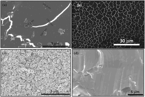
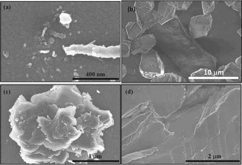
Subsequently, amorphous carbon thin films were irradiated with nanosecond ArF excimer laser (laser wavelength = 193 nm, pulse duration = 20 ns) using laser energy density 0.6–1.0 J cm−2. The pulse laser annealing technique melts the carbon film in a highly super undercooled state, which is followed by quenching to complete the whole process within 200–250 ns. This leads to the conversion of amorphous carbon films into Q-carbon or diamond. The formation of Q-carbon requires higher undercooling than diamond, which can be manipulated by controlling laser, substrate, and film variables. Thermal conductivities of the film and the substrate play a critical role in determining the degree of undercooling and the quenching rate. We have used the previously developed SLIM software to simulate and control the details of laser–solid interactions [Citation7]. Figure shows Gibbs free energy versus temperature for graphite (Gg), liquid carbon (Gliq), and diamond (Gd). The diamond is formed at Td where Gliq and Gd intersect with undercooling of (Tgl − Td), and Q-carbon is formed at a lower undercooling (Tgl − T*). The diamond was found to nucleate from Q-carbon, particularly at triple points. To form Q-BN, nanocrystalline (average grain size 20 nm) were deposited by KrF laser (laser wavelength = 248 nm, pulse duration = 25 ns, and energy density = 3.0–3.5 J cm−2) and annealed subsequently by ArF laser (laser wavelength = 193 nm, pulse duration = 20 ns, and energy density = 0.6–1.0 J cm−2). Figure shows the formation of Q-carbon composite (a), large-area Q-carbon (b), microdiamonds (c), and large-area single-crystal films (d).
Figure 1. Gibbs free energy vs. temperature for graphite (Gg), liquid carbon (Gliq), and diamond (Gd).
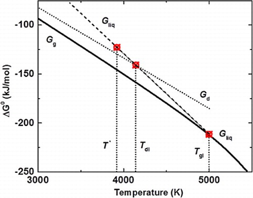
Figure 2. (a) Formation of Q-carbon and growth of diamond from Q-carbon, (b) large-area Q-carbon, (c) microcrystals of diamond, and (d) large-area single-crystal diamond film on (0001) sapphire.
The characterization of Q-diamond, Q-carbon, and Q-BN was carried out using Raman spectroscopy, X-ray photoelectron spectroscopy (XPS), Secondary-ion mass spectrometry (SIMS), electron energy-loss spectroscopy (EELS), field emission scanning electron microscopy (FESEM), and superconducting quantum interference device (SQUID) magnetometry. Alfa300 R superior confocal Raman spectroscope with a lateral resolution less than 200 nm was employed to characterize the Raman-active vibrational modes. Crystalline Si was used to calibrate the Raman spectra, which has its characteristic Raman peak at 520.6 cm−1. High-resolution SEM with sub-nanometer resolution was carried out using FEI Verios 460L SEM to characterize the as-deposited and the laser-irradiated films. High-resolution SEM measurements were carried out using the field emission mode in FEI Verios 460L SEM. FEI Quanta 3D FEG with dual beam technology employing both electron and ion beam guns was used for preparing cross-sectional TEM samples. A low energy ion beam (5 kV, 10 pA) was used to clean up the focused ion beam (FIB) surface damage. Aberration-corrected STEM-FEI Titan 80-300 was used in conjunction with EELS (with a resolution of 0.15 eV) to acquire high angle annular dark field (HAADF) images and EELS spectra of Q-diamond, Q-carbon, and Q-BN thin films. The electron probe current used in the experiment was 38 ± 2 pA. The EELS data were acquired with a collection angle of 28 mrads. We have used a Modulated Nanoindentation (MoNI) technique to measure the stiffness and effective Young’s modulus. Nanoindentation combined with finite element modeling has been used to measure hardness of Q-carbon, and results compared with similar measurements on diamond, sapphire, and SiC at the same time. In the atomic force microscopy (AFM)-based MoNI [Citation8] technique, force is measured as a function of indentation depth and slope is used to extract stiffness of Q-carbon films [Citation9].
Results and discussion
Atomic structure of Q-carbon and relation to diamond
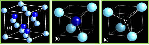
Figure (a) shows the unit cell of the diamond cubic lattice (DCL). It is interesting to note that DCL unit cell consists of two subunit cells D1 (Figure (b)) and D2 (Figure (c)). The D1 is basically a diamond tetrahedron enclosed in (a/2,a/2,a/2), one eighth of the unit cell. The D2 is similar to D1, but the central atom is missing. The number density of atoms in D1 is 12/a3, compared to 4/a3 in D2, and 8/a3 in a standard DCL. Thus, four D1 and four D2 subunit cells alternate to form the unit cell of DCL. In a crystalline lattice, outer atoms of D1 unit cell are shared by eight subunit cells, but only four covalent bonds. However, in a random packing of these tetrahedra, the outer atoms are shared by four atoms, and thus the effective number of atoms increases from 1.5 to 2.0. Molten carbon is metallic and where atoms are closely packed and upon quenching, randomly packed tetrahedra are observed. The formation of these tetrahedral amorphous structures is evidenced by the radial distribution function having intensity peaks at 0.154 and 0.252 nm in the selected-area electron diffraction pattern of Q-carbon. It has been shown that tetrahedra can be randomly packed to a packing efficiency of 80%, which leads to an effective increase in number density of atoms [(16/a3 × 0.8)/(8/a3)] in Q-carbon by 60% over that of diamond. Since two or three of these tetrahedra can be joined through 90° rotation, it is possible to create distinct phases of Q3, Q2, and Q1 by packing randomly units of three, two, and one tetrahedra, respectively. The number density of atoms in these units remains the same (16a−3), but the packing fraction may change the overall number density of atoms and properties related to it. For B-doped Q-carbon, corresponding three distinct phases (QB3, QB2, and QB1) of high-temperature superconductivity have been identified, as discussed later in this review. The atomic structure modeling of Q-carbon is used to explain novel properties, including enhanced hardness and high-temperature superconductivity [Citation10].
Figure 3. (a) Atomic structure of DCL, (b) subunit cell (D1), and (c) subunit cell (D2).
Enhanced hardness of Q-carbon, harder than diamond
The materials upon external loading undergo elastic (reversible) and plastic (irreversible) deformation through generation of dislocations. The stiffness of a material is related to resistance to volume compression (bulk modulus, B) and/or resistance to linear compression (Young’s modulus, E). The bulk modulus B is related to Young’s modulus through Poisson’s ratio (υ), B = E/(3(1 − 2υ)). Poisson’s ratio is the measure of transverse contraction to longitudinal extension. The hardness (H), on the other hand, is related to plastic deformation and shear modulus (µ) as H = 0.151 µ, which is related to Young‘s modulus as µ = E/(2(1 + υ)). This shows that Poisson’s ratio plays a critical role in maintaining the high shear modulus and hardness of materials. The shear modulus increases with the decrease of Poisson’s ratio, whereas the bulk modulus increases with the increase of Poisson’s ratio. Thus, an optimum value of hardness is achieved when Poisson’s ratio is 0.125, where bulk modulus is close to the shear modulus. The Poisson’s ratio of diamond (0.115) is close to this value, which makes diamond an ideal superhard material. Highly directional covalent bonding in diamond-related materials is able to resist both elastic and plastic deformation, leading to higher stiffness as well as higher hardness. To design materials harder than diamond, we have adopted a new strategy, where we increase the number density of atoms, and preserve sp3 and sp2 bonded strong covalent bonds. By randomly packing the tetrahedra with a packing efficiency of over 80%, we achieve over 60% higher number density of atoms, resulting in over 70% higher hardness than diamond.
Using a semiempirical approach, the bulk modulus B is modeled as a function of bond length for elements near the center of the periodic table for group IV, III–V, and II–VI tetrahedrally bonded homogeneous materials [Citation11]. According to this approach, B (in GPa) can be expressed as B = (Nc/4) (1972 − 220I)/d3.5, where Nc is the coordination number and d (in Å) is bond length. The ionicity parameter I accounts for charge transfer across the bond and its value is estimated as 0, 1, and 2 for group IV, III–V, and II–VI solids, respectively. Thus, I is equal to 1 in covalently bonded c-BN. We have modified this formula to relate bulk modulus with the number density of atoms. The bulk modulus can be expressed as B = (Nc/4) (3265 − 364I)Nd1.17, where Nd is number density of atoms (in Å−3), and B = (Nc/4) (98 − 10I)ρ1.17, where ρ is the mass density in g cm−3. The highest hardness of diamond is associated with its highest number density of atoms 1.76 × 10²³ atoms cm−3, which are covalently bonded. Using this value of Nd for diamond, bulk modulus (B) is calculated as 440 GPa and Young’s modulus as 1015 GPa. The corresponding values for Q-carbon are estimated as 761 GPa for bulk modulus, 1759 GPa for Young’s modulus, and 789 GPa for shear modulus. Table provides a summary of experimental and theoretical values of Young’s modulus (E), bulk modulus (B), Poisson’s ratio (υ), and shear modulus (µ), which is directly related to hardness.
Table 2. Experimental and theoretical values of Young’s modulus (E), bulk modulus (B), Poisson’s ratio (υ), and shear modulus (µ) directly related to hardness.
Figure shows force versus indentation depth curves for Q-carbon and a comparison with CVD (111) diamond films and bulk (0001) sapphire substrate. The nanostiffness measurements were made using MoNI technique combined with finite element modeling. The technique allowed the experimental measurement of the local perpendicular-to-the-plane elastic modulus of thin films at 0.01 nm depth resolution. The indentation depth d is related contact Young’s modulus (E*) by
(1)
where F is the normal force and R is the tip radius.
Figure 4. (a) Topography of Q-carbon filaments formed on a diamond-like carbon (DLC) film. (b) Topography of a filament cross-section; markers indicate positions across the filament where indentation measurements are conducted. (c) Indentation curves measured on the Q-carbon filament. Blue and red lines are measurements performed on the Q-carbon filament and the surrounding DLC film, respectively. Numbers refer to positions identified in (b) [Citation9].
![Figure 4. (a) Topography of Q-carbon filaments formed on a diamond-like carbon (DLC) film. (b) Topography of a filament cross-section; markers indicate positions across the filament where indentation measurements are conducted. (c) Indentation curves measured on the Q-carbon filament. Blue and red lines are measurements performed on the Q-carbon filament and the surrounding DLC film, respectively. Numbers refer to positions identified in (b) [Citation9].](/cms/asset/88c8cb98-7204-45d6-8f79-011aed537351/tmrl_a_1458753_f0004_c.jpg)
The measured Young’s modulus (E*) is related to Poisson‘s ratio (υ) and Young modulus of the tip (Et) and substrate (Es) by
(2)
Using these measurements (Figure ), we obtained effective stiffness (Young’s modulus) of Q-carbon as 1702 ± 138 GPa, compared to 1015 ± 107 GPa for diamond and 350 ± 30 GPa for sapphire. Using this value of E, for diamond υ is estimated to be 0.115 [Citation9]. Using this value of υ, the shear moduli of diamond and Q-carbon are estimated to be 455 and 789 GPa, respectively. This will lead to over 70% higher hardness for Q-carbon than diamond. Figure also shows an AFM image of surface topology of Q-carbon embedded in diamond-like carbon after laser annealing. The high-resolution image shows a considerable shrinkage as result of melting. The indentation curves were measured on Q-carbon (3, 4, and 5) and compared with diamond-like carbon (curves 1, 2, 6, and 7).
Figure 5. The experimentally measured Young’s modulus of Q-carbon as 1702 ± 138 GPa, compared to 1015 ± 107 GPa for diamond and 350 ± 30 GPa for sapphire [Citation9].
![Figure 5. The experimentally measured Young’s modulus of Q-carbon as 1702 ± 138 GPa, compared to 1015 ± 107 GPa for diamond and 350 ± 30 GPa for sapphire [Citation9].](/cms/asset/07374574-cf3f-4749-821d-05f270ee84c2/tmrl_a_1458753_f0005_c.jpg)
Ferromagnetism and extraordinary Hall Effect in Q-carbon
Undoped Q-carbon shows ferromagnetism with coercivity ∼150 Oe at 300 K, which increases to ∼200 Oe at 10 K. It is interesting to note that saturation magnetization in M versus H curve (Figure ) decreases only slightly less than 10% with temperature between 10 and 300 K. From the M versus H and M versus T measurements, Curie temperature was estimated over 570 K. Undoped Q-carbon exhibits n-type conductivity and extraordinary Hall Effect. The origin of intrinsic ferromagnetism in Q-carbon is due to the electronic mixing of sp2 and sp3 orbitals during its formation. Some of the unpaired electrons remain in the Q-carbon structure, which render it to be ferromagnetic in nature. Further work is needed to understand the three-dimensional coupling mechanism of these spins to create ferromagnetism. The temperature-dependent magnetic anisotropy constant calculations in Q-carbon indicate a nonlinear dependence with an exponent value of 2.03 which is attributed to the presence of a mixture of sp2-sp3 hybridized states. The temperature-dependent saturation magnetization curve of Q-carbon follows the modified Bloch’s law with the Bloch exponent equal to 2.04, pre-factor of 3.02 × 10⁻⁶ K−2.04 and a Curie temperature of 570 K [Citation12]. The negative values of the ordinary Hall coefficient in the temperature range 10–300 K indicate that the electron band is more conducting than the hole band in Q-carbon. An exponent value of 1.95 ± 0.05 that has been extracted from the Hall Effect measurements in Q-carbon suggests that the electron scattering in the Hall resistivity in Q-carbon follows a nonclassical ‘side-jump mechanism’. This electronic scattering mechanism exists in Q-carbon due to the presence of nonconducting centers which distort the wave function and create a local current density.
Figure 6. M vs. H plots of Q-carbon at different temperatures (10, 50, 100, 200, and 300 K) showing ferromagnetic characteristics. The upper inset shows magnetic force microscope (MFM) image of Q-carbon at 300 K. The lower right inset shows the diamagnetic signal from as-deposited DLC and the lower left inset shows finite coercivity (∼100 Oe) at 100 K.
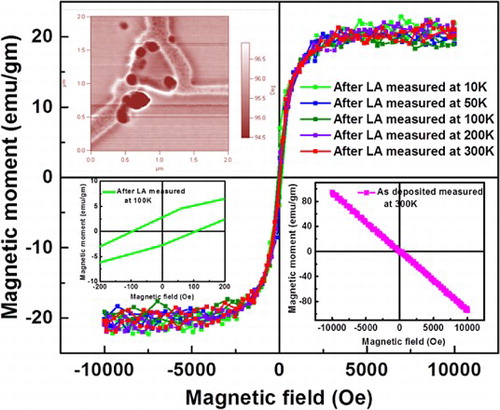
There is also an increase in the intensity and full width at half maximum (FWHM) of the π* peak in Q-carbon in the EEL spectrum as compared to the as-deposited DLC or diamond. This indicates an increase in the electronic density of the dangling bonds (present near the Fermi level) leading to exciting magnetic and electrical properties in Q-carbon [Citation12].
Doping with n- and p-type dopants
Diamond can be doped with p-type dopants, but doping with n-type dopants has presented a big challenge. In our new technique, dopants are mixed in the liquid state and quenched rapidly. Rapid quenching allows incorporation of dopant concentrations far in excess of thermodynamic solubility limits through the phenomenon of solute trapping. Higher dopant concentrations shift dopant energy levels closer to band edges and thus enhance ionization efficiencies. This is a critical aspect of doping with higher concentrations, as deep donors and acceptors at low concentrations provide much smaller concentrations of free careers.
For n-type doping, N-doped amorphous carbon films were deposited from the carbon target by PLD, while bombarding the growing carbon film with low energy (0.5 keV) of N2+ ions. The N-doped amorphous carbon films are melted to create a variety of structures in the form of nanodots, microdots, nanoneedles, microneedles, and large-area single-crystal films. The epitaxial structures of diamond are grown on practical substrates such as sapphire and silicon via domain matching epitaxy, where integral multiples lattice planes match across the film/substrate interface. For p-type doping, alternate layers of amorphous B and C are deposited with thicknesses adjusted according to dopant concentrations as desired. Figure (a) shows a diamond p–n junction, where n-doped diamond was grown by laser annealing (melting) of N-doped amorphous carbon. The next layer on the top of N-doped diamond is B-doped amorphous carbon layer, which is deposited selectively and laser annealed to create p–n junctions, as shown in the inset of Figure (a). The I-V plot from with low turn-on voltage of 3 V and a minimum of reverse bias current shows superior diode characteristics. The temperature-dependent I-V plots also show the characteristic diode behavior. With the increase in temperature, there is an increase in the forward bias current. This occurs due to increased concentration of charge carriers with an increase in temperature. The ideality factor of the p–n junction can be calculated using the diode equation Equation(3)(3) :
(3)
where, n, kB, T, VA, and I0 denote ideality factor, Boltzmann constant, temperature (of the p–n junction), applied voltage, and reverse saturation current, respectively. I0 and n are calculated to be ∼1.0E-9 A and 2.077, respectively. The value of ideality factor is close to 2 which indicates that the fabricated diode is close to an ideal one. We have also fabricated N-V (nitrogen-vacancy) doped nanodiamonds [Citation13] with size ranging from 4 to 8 nm. Figure (a) shows photoluminescence (PL) versus energy spectra of as-deposited N-doped amorphous carbon film, and this film after annealing with 0.6 J cm−2 ArF laser pulse. The PL spectrum shows sharp zero phonon line (ZPL) peaks to NV− (at 637 nm or 1.95 eV) and NV0 (at 537 nm/2.16 eV). The inset also shows transitions from these centers when the sample is irradiated with 532 nm PL source exciting both NV− and NV0 centers.
Figure 7. (a) I-V characteristics showing diamond p–n junction with the inset showing a schematic of the diode device (electrodes, B-doped diamond, and N-doped diamond); and (b) I-V characteristics at different temperatures (100, 300, and 350 K) with the inset showing the ideality factor = 2.077.
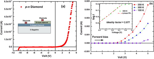
Figure 8. (a) PL of NV diamond at 300 K, and (b) time-resolved PL spectroscopy of NV diamond. The insets in (a) show SEM image and PL emission (at 532 nm excitation) of NV diamonds.
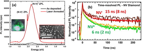
Figure (b) shows time-resolved PL measurements using 415-nm 200-fs excitation of NV nanodiamond samples. A significant increase in decay time over 200% compared to NV centers processed by current techniques is observed, demonstrating the high quality of NV centers processed by our techniques. We have shown that the transitions between NV− and NV0 centers can be driven electronically, photonically, and thermally in a controlled way for a variety of applications from atomic sensors and biomarkers to quantum computing and communication.
High-temperature superconductivity in B-doped Q-carbon
Superconductivity in carbon-based strongly bonded materials has generated a tremendous interest because they provide an ideal platform for high-temperature superconductivity [Citation14]. For strongly coupled materials, superconducting transition temperature, , where λ is the electron–phonon coupling constant related to ratio of spring constants, ω is averaged phonon frequency, M is averaged atomic mass, and η is the McMillan–Hopfield parameter with units of spring constant and is related to strength of electronic response of electrons near the Fermi surface to atomic perturbations. Thus, using this as a guideline, the search for higher Tc needs to focus on sp3 and sp2 strongly bonded carbon-based materials, which are doped with appropriate dopants to provide free carriers.
Distinct phases of B-doped Q-carbon are formed when B-doped and undoped diamond tetrahedra are packed randomly. By changing the ratio of doped to undoped tetrahedra, distinct phases of B-doped Q-carbon with concentration varying from 5.0% to 50.0% can be synthesized [Citation10]. We have synthesized three distinct phases of amorphous B-doped Q-carbon, which exhibit record high-temperature superconductivity following Bardeen–Cooper–Schrieffer (BCS) mechanism, as shown in the HAADF image (Figure ). First phase has B concentration ∼17% with superconducting transition temperature (Tc) = 37 K (QB1) [Citation15,Citation16], second phase has B concentration ∼25% with Tc = 56 K (QB2) [Citation17], and third phase has B concentration ∼50% with Tc expected over 100 K (QB3), as shown in HAADF image in Figure . From geometrical modeling, we derive that the QB1 consists of randomly packed tetrahedra, where one out of every three tetrahedra contains a B atom in the center which is sp3 bonded to four carbon atoms. The QB2 consists of randomly packed tetrahedra, where one out of every two tetrahedra contains a B atom in the center which is sp3 bonded to four carbon atoms. The QB3 consists of randomly packed tetrahedra, where every tetrahedron contains a B atom in the center which is sp3 bonded to four carbon atoms. We present detailed high-resolution TEM results on structural characterization, and EELS and Raman spectroscopy on dopant spatial distribution and bonding characteristics of B and C atoms. These results on structure, B concentration and sp3/sp2 bonding are correlated with high-temperature superconducting properties. It is found that high-temperature superconductivity in B-doped Q-carbon is derived primarily from high-number density of states near the Fermi level, while keeping the electron–phonon coupling reasonably high. The formation of distinct superconducting phases (QB1, QB2, and QB3) in B-doped amorphous Q-carbon and corresponding Q1, Q2, and Q3 phases in undoped Q-carbon [Citation10] provide the first evidence for polyamorphism in amorphous tetrahedrally bonded Q-carbon, formed after quenching from a super undercooled state. This is analogous to polymorphism in crystalline solids. The number density of atoms in these phases will depend upon the packing efficiency of one, two, and three units of D1 tetrahedra. The polyamorphism has been shown to occur under high pressure in tetrahedrally bonded amorphous silicon [Citation18,Citation19] and supercooled aqueous solutions [Citation20].
Figure 9. (a) EELS of amorphous B, intermediate superconducting layer (QB3), second superconducting phase (QB2), (b) HAADF image of B-doped Q-carbon, (c) B concentration profile, and (d) C concentration profile [Citation17].
![Figure 9. (a) EELS of amorphous B, intermediate superconducting layer (QB3), second superconducting phase (QB2), (b) HAADF image of B-doped Q-carbon, (c) B concentration profile, and (d) C concentration profile [Citation17].](/cms/asset/b2b636e9-006d-48e7-9ac6-b22d050c9257/tmrl_a_1458753_f0009_c.jpg)
Enhanced field emission
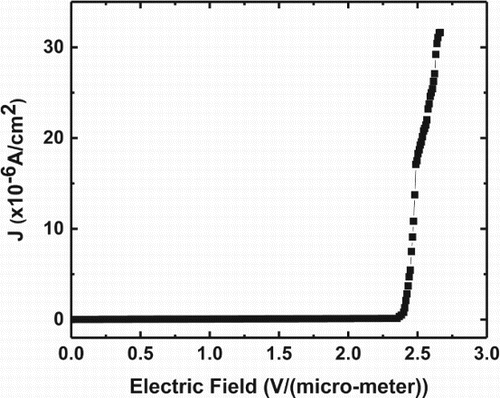
Diamond because of its negative electron affinity exhibits enhanced field emission and has been considered for a variety of field emission devices. The field emission from nanodots and nanoneedles is considerably enhanced. Our technique is ideal for the formation of nanodots and nanoneedles (as shown in Figure (a)) and Raman spectra of nanoneedles [Citation21] (as shown in Figure (b)). These structures can be grown epitaxially so that all of them have exactly the same orientation [Citation22]. The crystalline orientation plays a critical role in field emission efficiency. However, the field emission in Q-carbon is further enhanced due its higher negative electron affinity compared to diamond. The field emission measurements from Q-carbon are shown in Figure with a turn-on voltage of 300 V. This field emission follows the Fowler–Nordheim model. The emission current can be multiplied by four orders of magnitude, thereby generating over 10,000 electrons for every electron in the current. The turn-on field (ETO) required to draw an emission current density of 1 µA/cm2 is found to be 2.65 V/µm. The Q-carbon films show a good stability during the field emission measurements. The microstructure and morphology of the field emitting Q-carbon film was analyzed by a range of techniques such as field emission scanning electron microscope, Raman spectroscopy, and AFM. Optimum values of sp3 and sp2 bonding in carbon structures are needed for efficient field emission from carbon-based field emitters. The Q-carbon structure consists of around 85% sp3 and rest sp2 bonded carbon atoms to achieve highly efficient field emission properties. The outstanding field emission property from Q-carbon is attributed to the unique sp2/sp3 mixture in the emitter, conductive grain boundaries inside a Q-carbon cluster, local field enhancement due to the geometry of the grains, and the presence of sp2-rich semimetallic alpha carbon matrix in the film. The film demonstrates hysteresis-free very high emission stability, meaning very low fluctuation at high current density over hours during the operation with no generation of defects during the successive emission measurements. Our findings thus hold great promise for the development of Q-carbon films in application domains such as field emitters and heterostructures for novel micro- and nano-electronic devices.
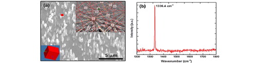
Figure 10. (a) SEM image of nanodots and nanoneedles, and (b) Raman spectra of nanoneedles showing the sharp diamond peak at 1336.4 cm−1. The inset in (a) shows the characteristic Kikuchi pattern (using electron backscatter diffraction (EBSD)) of diamond.
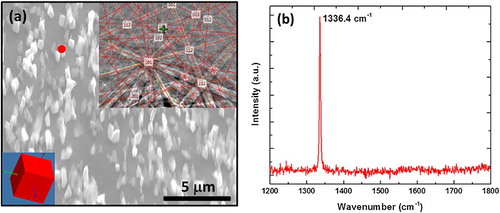
Figure 11. Field emission of Q-carbon thin film (J-E characteristics). The turn-on field (ETO) required to draw an emission current density of 30 µA/cm2 is found to be 2.65 V/µm. This field emission follows the Fowler–Nordheim model.
Direct conversion of h-BN into Q-BN or c-BN
Our studies on laser annealing of nanocrystalline pure h-BN show that molten BN can be quenched into Q-BN or c-BN depending upon the undercooling [Citation23]. There are a lot of similarities between amorphous carbon conversion and nanocrystalline h-BN conversion. However, there are some differences such as amorphous carbon has a mixture of sp3 and sp2 compared to pure h-BN phase. Our numerical simulations clearly show that thermal conductivities of the film and the substrate play a critical role in the undercooling, and conversion into Q-BN or c-BN.
It should be pointed that our process produces phase-pure c-BN. Figure shows the formation of c-BN and Q-BN (a), large microcrystals of phase-pure c-BN (b), microcrystals of c-BN (c), and large-area epitaxial single-crystal films (d). The twinning content of c-BN microcrystallites can be controlled by quenching rates. The spacing and number density of twins have been shown to enhance hardness. Our recent studies on Q-BN also indicate it to be harder than diamond.
Figure 12. (a) Formation of c-BN from Q-BN, (b) large microcrystals of phase-pure c-BN, (c) microcrystals of c-BN, and (d) large-area epitaxial single-crystal films.
Summary
We have shown that amorphous carbon can be converted into Q-carbon and diamond, h-BN into Q-BN and c-BN at ambient temperature and pressure in the form of nanodots and microdots, nanoneedles and microneedles, and large-area single-crystal films. We have created three distinct phases of undoped Q-carbon (Q1, Q2, and Q3), and corresponding B-doped high-temperature superconducting (QB1, QB2, and QB3) phases with record BCS transition temperatures. These structures can be doped with both n- and p-type dopants with concentrations far exceeding the equilibrium solubility limits though solute trapping phenomena. Undoped Q-carbon exhibits robust ferromagnetism with extraordinary Hall Effect, highest Young’s modulus and hardness (70% higher than diamond), and enhanced field emission. A MoNI technique has been used to measure effective stiffness (Young’s modulus) of amorphous Q-carbon as 1702 ± 138 GPa, compared to 1015 ± 107 GPa for (111) diamond and 350 ± 30 GPa for (0001) sapphire. Since the number density of atoms in the diamond tetrahedra is 60% higher than the overall density of atoms in the DCL, we estimate Q-carbon hardness, using a semiempirical approach, to be over 70% higher than that of diamond, in agreement with experimental results. Upon doping with boron, Q-carbon turns from n-type into p-type and exhibits high-temperature superconductivity with Tc over 55 K and higher. The Tc is increasing with increasing boron concentration, and B-doped Q-carbon with 50 at% boron has been synthesized with Tc predicted to be higher than 100 K. Thus, B-doped Q-carbon provides an ideal platform for high-temperature superconductivity in view of light masses, strong bonding, and higher packing efficiency than diamond. The formation of distinct high-temperature superconducting phases provides a direct evidence for polyamorphism in amorphous Q-carbon, which are formed under a super undercooled state [Citation10].
Acknowledgements
We are grateful to Fan Family Foundation Distinguished Chair Endowment for Professor J. Narayan. Ritesh Sachan acknowledges the National Academy of Sciences (NAS), USA for awarding the NRC research fellowship. We are also very pleased to acknowledge the technical help and useful discussions with Professors Marvin Cohen, Elisa Riedo, John Prater, and Roger Narayan.
Disclosure statement
No potential conflict of interest was reported by the authors.
Additional information
Funding
References
- Narayan J, Godbole VP, White CW. Laser method for synthesis and processing of continuous diamond films on nondiamond substrates. Science. 1991;252:416–418. [cited 2015 Jul 27]. Available from: http://www.sciencemag.org/content/252/5004/416.abstract. doi: 10.1126/science.252.5004.416
- Mirkarimi PB, McCarty KF, Medlin DL. Review of advances in cubic boron nitride film synthesis. Mater Sci Eng R Reports. 1997;21:47–100. [cited 2016 Jun 19]. Available from: http://linkinghub.elsevier.com/retrieve/pii/S0927796X97000090. doi: 10.1016/S0927-796X(97)00009-0
- Bundy FP, Bassett WA, Weathers MS, et al. The pressure-temperature phase and transformation diagram for carbon; updated through 1994. Carbon. 1996;34:141–153. [cited 2015 Jul 27]. Available from: http://www.sciencedirect.com/science/article/pii/0008622396001704. doi: 10.1016/0008-6223(96)00170-4
- Samantaray CB, Singh RN. Review of synthesis and properties of cubic boron nitride (c-BN) thin films. Int Mater Rev. 2005;50:313–344. [cited 2016 Jun 19]. Available from: http://www.tandfonline.com/doi/full/10.1179/174328005X67160.
- Narayan J, Bhaumik A. Novel phase of carbon, ferromagnetism, and conversion into diamond. J Appl Phys. 2015;118:215303. [cited 2015 Dec 2]. Available from: http://scitation.aip.org/content/aip/journal/jap/118/21/10.1063/1.4936595.
- Narayan J, Bhaumik A. Research update: direct conversion of h-BN into pure c-BN at ambient temperatures and pressures in air. APL Mater. 2016;4:020701. [cited 2016 Feb 23]. Available from: http://scitation.aip.org/content/aip/journal/aplmater/4/2/10.1063/1.4941095].
- Singh RK, Narayan J. A novel method for simulating laser-solid interactions in semiconductors and layered structures. Mater Sci Eng B. 1989;3:217–230. [cited 2015 Apr 18]. Available from: http://www.sciencedirect.com/science/article/pii/0921510789900147. doi: 10.1016/0921-5107(89)90014-7
- Gao Y, Kim S, Zhou S, et al. Elastic coupling between layers in two-dimensional materials. Nat Mater. 2015;14:714–720. [cited 2017 Nov 24]. Available from: http://www.nature.com/doifinder/10.1038/nmat4322.
- Narayan J, Gupta S, Bhaumik A, Sachan R, Cellini F, Riedo, E. Q-carbon harder than diamond. MRS Comm. 2018. doi: 10.1557/mrc.2018.35.
- Narayan J, Bhaumik A, Sachan R. High temperature superconductivity in distinct phases of amorphous B-doped Q-carbon. J Appl Phys. 2018;123(14). (accepted)
- Liu AY, Cohen ML. Prediction of new low compressibility solids. Science. 1989;245:841–842. [cited 2017 Nov 24]. Available from: http://www.ncbi.nlm.nih.gov/pubmed/17773359. doi: 10.1126/science.245.4920.841
- Bhaumik A, Nori S, Sachan R, et al. Room-temperature ferromagnetism and extraordinary Hall Effect in nanostructured Q-carbon: implications for potential spintronic devices. ACS Appl Nano Mater. 2018;1:807–819. [cited 2018 Mar 17]. Available from: http://pubs.acs.org/doi/10.1021/acsanm.7b00253.
- Narayan J, Bhaumik A. Novel synthesis and properties of pure and NV-doped nanodiamonds and other nanostructures. Mater Res Lett. 2016;5:1–9. [cited 2016 Dec 22]. Available from: https://www.tandfonline.com/doi/full/10.1080/21663831.2016.1249805.
- Moussa JE, Cohen ML. Constraints on Tc for superconductivity in heavily boron-doped diamond. Phys Rev B. 2008;77:2. [cited 2017 Jan 23]. Available from: http://link.aps.org/doi/10.1103/PhysRevB.77.064518.
- Bhaumik A, Sachan R, Narayan J. High-Temperature superconductivity in boron-doped Q-carbon. ACS Nano. 2017;11:5351–5357. [cited 2017 Jul 13]. Available from: http://pubs.acs.org/doi/abs/10.1021/acsnano.7b01294.
- Bhaumik A, Sachan R, Narayan J. A novel high-temperature carbon-based superconductor: B-doped Q-carbon. J Appl Phys. 2017;122:045301. [cited 2017 Aug 11]. Available from: http://aip.scitation.org/doi/10.1063/1.4994787.
- Bhaumik A, Sachan R, Gupta S, et al. Discovery of high-temperature superconductivity (T c = 55 K) in B-doped Q-carbon. ACS Nano. 2017. doi:10.1021/acsnano.7b06888. [cited 2017 Nov 19]. Available from: http://pubs.acs.org/doi/10.1021/acsnano.7b06888.
- Morishita T. High density amorphous form and polyamorphic transformations of silicon. Phys Rev Lett. 2004; 93:1055. [cited 2018 Mar 17]. Available from: https://link.aps.org/doi/10.1103/PhysRevLett.93.055503.
- McMillan PF, Wilson M, Daisenberger D, et al. A density-driven phase transition between semiconducting and metallic polyamorphs of silicon. Nat Mater. 2005;4:680–684. [cited 2018 Mar 17]. Available from: http://www.nature.com/articles/nmat1458. doi: 10.1038/nmat1458
- Woutersen S, Ensing B, Hilbers M, et al. A liquid-liquid transition in supercooled aqueous solution related to the HDA-LDA transition. Science. 2018;359:1127–1131. [cited 2018 Mar 17]. Available from: http://www.sciencemag.org/lookup/doi/10.1126/science.aao7049.
- Prawer S, Nemanich RJ. Raman spectroscopy of diamond and doped diamond. Philos Trans R Soc London A Math Phys Eng Sci. 2004;362:2537–2565. [cited 2017 Apr 4]. Available from: http://rsta.royalsocietypublishing.org/content/362/1824/2537.long. doi: 10.1098/rsta.2004.1451
- Narayan J, Bhaumik A. Q-carbon discovery and formation of single-crystal diamond nano- and microneedles and thin films. Mater Res Lett. 2016;4:118–126. [cited 2017 Apr 6]. Available from: http://www.tandfonline.com/doi/full/10.1080/21663831.2015.1126865.
- Narayan J, Bhaumik A, Xu W. Direct conversion of h-BN into c-BN and formation of epitaxial c-BN/diamond heterostructures. J Appl Phys. 2016;119:185302. [cited 2017 Jul 13]. Available from: http://aip.scitation.org/doi/10.1063/1.4948688.