
ABSTRACT
Inorganic cesium lead halide perovskite nanowires (NWs) were synthesised by an in-plane self-assembly method. With the assistance of saturated solvent vapour, perovskite microparticles self-assembled into NWs. By stoichiometric adjustment of the halogen anion components in the NWs, their photoluminescence could be tuned to span the entire visible range. A detailed investigation of the lasing properties of the in-situ perovskite NWs and microplates revealed a lasing range of 420–560 nm, with typical thresholds of 18.8 μJ cm−2 for CsPbBr3 NWs and 8.87 μJ cm−2 for CsPbBrxCl3-x microplates. The NWs exhibited robust stability under extended laser pumping in ambient atmosphere.
GRAPHICAL ABSTRACT
IMPACT STATEMENT
An in-plane self-assembly method was developed for high-quality CsPbX3 nanowires preparation, and the NWs possessed robust lasing performance in the range of 420–560 nm.
KEYWORDS:
1. Introduction
As direct bandgap semiconductors that exhibit high quantum yields, optical gains, and ease of band engineering, methylamine/formamidine/cesium lead halide perovskites (MA/FA/CsPbX3, where X = halogen) [Citation1–8] are considered promising candidates as light sources in applications such as light emitting diodes (LEDs) [Citation1,Citation4], nanolasers [Citation1,Citation5,Citation6], and bioimaging [Citation9]. Semiconductor nanowire (NW) lasers, owing to their compact size, highly coherent output, and efficient optical confinement, are essential building blocks for optoelectronic devices and integrated photonic systems [Citation10,Citation11]. Each NW can serve not only as a gain medium but also a Fabry-Pérot (F-P) cavity for stimulated emission [Citation10,Citation11]. Perovskite NWs are one of the most promising materials for realising low-threshold, high quality factor nanolasers with broadband tuneability (400–780 nm) via halogen anion tuning [Citation4–6]. Recently, lasing from cesium lead bromide perovskite NWs pumped by a continuous-wave laser has been realised [Citation12].
To date, inorganic/organic lead halide perovskite NW fabrication methods can be roughly categorised as vapour-transfer [Citation13–16] or solution-processing [Citation17–23] methods, or a combination of both [Citation24]. By the vapour-transfer method, highly purified perovskite NWs can be obtained; however, this method suffers the disadvantage of high energy consumption. For the solution-processing method, NWs of lead salts such as lead acetate [Citation17–19] or lead iodide [Citation20,Citation21] are frequently used as templates to react with MAX/(FAX-MAX)/CsX solutions, from which the corresponding MAPbX3/(FA-MA)PbX3/CsPbX3 NWs can be obtained. Although the solution-processing method is relatively simple, the fabricated perovskite NWs are easily gathered in clusters comprising nanowires, nanoparticles, and nanoplates [Citation13–24]. Furthermore, for device fabrication, the NWs must undergo post-synthesis transfer to the desired substrate by micromanipulation, and during this process, the selected NWs can be easily damaged or broken.
In this work, we propose an in-plane self-assembly method to synthesise cesium lead halide perovskite NWs. Randomly dispersed perovskite microcrystals on the substrate can assemble into NWs under a saturated solvent-vapour atmosphere. By stoichiometric anion tuning, perovskite nanocrystals with single or dual halogen components can be realised, consequently the corresponding NWs can be obtained, which is different with some works, like ion-exchange [Citation17,Citation22,Citation24]. Different from other methods, the required dose of perovskite precursor is low to dozens of nanograms, which can reduce the pollution of toxic lead to environment; the obtained NWs are individually dispersed on the substrate and no NW clusters can be found, which means that no further transfer or micromanipulation is required. The NWs possess excellent crystallinity and broadband tuneability, and they can be easily lased under a suitable pulse laser.
2. Methods
2.1. Self-assembly of CsPbX3 NWs
Firstly, Cesium lead halide perovskite NCs were synthesised according to previous reports [Citation25,Citation26]. The cleaned NC sediment was dissolved in methanol at a concentration of 1.88 mM.
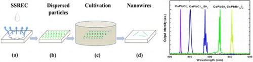
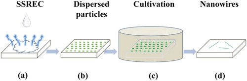
As depicted in Figure , the NW self-assembly process can be divided into two steps: substrate-supported rapid evapouration crystallization (SSREC) [Citation27] and cultivation [Citation28] in a saturated vapour environment. A typical CsPbBr3 NW preparation process was as follows: (1) The hydrophilic slide-glass substrate was heated by hot plate to 130°C. Then, the perovskite-methanol solution (50 μL) was dripped on the heated substrate using a micropipettor, shown in Figure (a). As the methanol rapidly evapourated, CsPbBr3 microcrystals crystallised randomly on the substrate, illustrated in Figure (b). (2) The sample was sealed in a Petri dish of 9 cm diameter containing methanol (150 μL) in Figure (c). The typical cultivating time was 7 days at 25°C. During cultivation, the micron-size perovskite particles underwent in-plane self-assembly, finally producing very well-structured NWs (Figure (d)). The concentration of solvent, evapouration temperature, cultivation time, and cultivation temperature affect the morphology of the NWs. For the other CsPbX3 samples, the NWs were obtained via the similar procedures with corresponding stoichiometric anions perovskite nanocrystals.
Figure 1. Schematic diagram of in-plane self-assembly method for perovskite NWs.
2.2. CsPbX3 NWs characterisations
The X-ray diffraction (XRD) patterns of the perovskite CsPbBr3 NWs were measured using a Bruker D8 ADVANCE diffractometer with a Cu Kα source. Scanning electron microscopy (SEM) images were obtained using a Phenom ProX desktop SEM. The transmission electron microscopy (TEM) and selected area electron diffraction (SAED) images were conducted with an FEI Tecnai G2F20 instrument operating at a voltage of 200 kV. The lasing performance was based on the objective stage of the optical microscope (Zeiss Axio Scope.A1). The 400 nm pumped source was second harmonic of the output of a Coherent RegA amplifier (800 nm, 35–50 fs, 1 kHz) seeded by a Coherent Mira oscillator. Emission from the NW was collected by an objective, 50×, NA = 0.75 (Zeiss, Epiplan). Optical images were obtained with a Retiga R6 CCD camera (QImaging Corporation), while spectra were acquired with a PG2000-Pro fibre spectrometer (IdeaOptics) with a spectral resolution of 1.5 nm. All lasing measurements were conducted at room temperature (24°C).
3. Results and discussions
3.1. Structure of CsPbX3 NWs
The synthesised CsPbX3 nanocrystals (NCs) ranged in diameter from 4 to 30 nm, as shown by the TEM images in Figure (a). After the SSREC process, randomly distributed perovskite micro-particles were obtained (Figure (b)). The particle sizes were sub-micron to micron in order, which is beneficial for the self-assembly process. The as-grown NWs were 2–100 μm in length and 0.3–1.5 μm in width, where the well-formed two facets can be confirmed from the SEM in Figure (c).
Figure 2. Structural characterisation of CsPbBr3 perovskite NCs and NWs. (a) TEM (scale bar, 50 nm) and (inset; scale bar, 5 nm) high-resolution TEM images of fresh NCs. (b) SEM image of well-dispersed NPs after SSREC (scale bar, 10 μm), with the local SEM of the NPs (inset; scale bar, 1 μm). (c) SEM image of a single NW on the substrate (scale bar, 2 μm). (d) XRD pattern of the as-grown CsPbBr3 NWs (black curve, top panel) in comparison with those of orthorhombic (red curve, middle panel) and cubic standards (blue curve, bottom panel). (e) TEM image of a CsPbBr3 NW (scale bar, 0.5 μm), with (inset) its SAED pattern (scale bar, 5 nm−1). (f) PL spectra of various CsPbX3 NW materials excited by a mercury lamp.
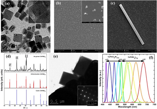
We investigated the NW crystal structure by XRD and SAED. The typical XRD patterns of the CsPbBr3 NWs (top panel, experimental; middle panel, theoretical for orthorhombic phase; bottom panel, theoretical for cubic phase) are shown in Figure (d). The diffraction peaks of the as-grown NWs are sharp and intense, indicating their highly crystalline nature. The obvious splitting of the narrow 004 and 220 peaks of our sample in the top panel of Figure (d) is indicative of the orthorhombic phase, which is obviously distinct from single peak of cubic phase in the bottom panel. The same conclusion can be validated by the TEM results in Figure (e). The SAED pattern indicates the NW’s single crystalline nature and can be indexed as the [220] zone axis of the orthorhombic phase. The growth direction of the NW was also indexed as the [004] direction of the orthorhombic phase. By controlling the ratio of halogen anions, various cesium lead halide perovskite NWs can be obtained by in-plane self-assembly. The PL of various NWs, excited by a mercury lamp, can span the entire visible range (420–690 nm), as shown in Figure (f). One interesting phenomenon is that the PL bands of pure halide NWs (for example CsPbCl3 and CsPbBr3) are narrower than those of mix-halide system. We speculate that wider band of PL in mix-halide system originates from the inhomogeneous replacement of halide components.
3.2. Lasing performance of CsPbX3 NWs
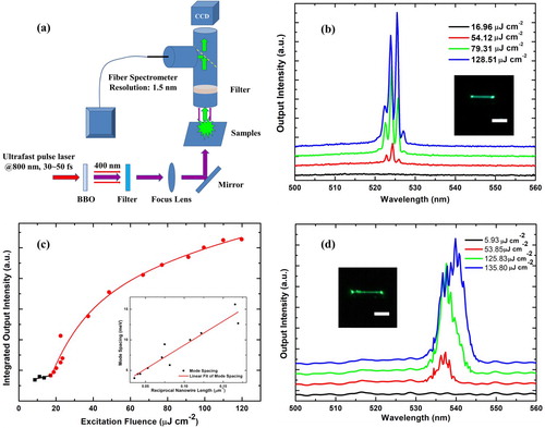
The smooth facets of the NW form a laser resonant cavity. The optical setup for NW lasing is shown in Figure (a). The PL intensity as a function of the excitation fluence for a 14-μm length of CsPbX3 NW is shown in Figure (b). As the excitation energy density increases, several peaks appear within the spontaneous spectral range. It is inferred that stimulated emission becomes predominant, and multi-stimulation modes are excited. The corresponding image was shown in the inset of Figure (b). The laser cavity quality factor (Q) can be defined by Q = λ/Δλ, where λ is the peak centre wavelength and Δλ is the FWHM. The Q factor of the strongest mode can be calculated as 584, using 525.5 nm as the peak centre and approximate 0.90 nm for Δλ. The power-dependence of the integrated output in Figure (c) depicts the transition from a spontaneous emission to the stimulated case. The lasing threshold value of 18.79 μJ cm−2 is obtained. Due to the low resolution of our fibre spectrometer (≈1.5 nm), the threshold value is higher than those previously reported [Citation13,Citation20,Citation24]. The linear dependence of the mode spacing with the inverse of the NW length indicates F-P lasing modes, as shown by the inset of Figure (c). The mode spacing ΔE obeys the rule, ΔE = hc (2n•L)−1, where h is the Planck constant, c is the speed of light, n is the group index of the perovskite NW, and L is the length of the sample. A longer NW (24.9 μm) can excite more lasing modes, where the corresponding wavelength space is approximate 1.0 nm according to the inset of Figure (c); however, due to the poor resolution of the spectrometer (1.5 nm), only an envelope of many lasing modes is observed (Figure (d)).
Figure 3. Lasing performance of perovskite CsPbBr3 NWs. (a) Diagram of lasing measurement set-up for perovskite NWs. (b) Power-dependent emission spectra from CsPbBr3 NW with length of ∼14 μm for various excitations from a femtosecond pulsed laser, with its optical image (inset). (c) The integrated output intensity of the CsPbBr3 NW with pumping fluence (discrete squares and circles), where the linear fit (black) and parabolic (red) curves correspond to spontaneous emission and stimulated cases, respectively; (inset) the mode spacing versus inverse NW length, where discrete circles (black) are experimental values and the solid curve (red) is the linear fit result. (d) Power-dependent emission spectra of a short CsPbBr3 NW, (inset) optical image of the same sample (length, 24.9 μm). Both scale bars for the optical images in (b) and (d) are 10 μm.
In Figure , we demonstrate the lasing results from hybrid perovskite CsPbBrxCl3-x samples. The typical threshold of a 7.3 μm long NW is 76.50 μJ cm−2, as shown in Figure (a). Multiple and equally spaced lasing peaks indicate high-quality F-P resonance in the NW. As the excitation fluence increases, the peak centre is blue-shifted from 488.8–487.5 nm (Figure (b)). The 1.3 nm blueshift could originate from electron–hole plasma, thermally induced bandgap, or refractive index changes, among others [Citation17,Citation20].
Figure 4. Lasing performance of hybrid CsPbX3 perovskite samples. (a) Power-dependent emission spectra of a short (7.3 μm) CsPbBrxCl3-x NW, (inset) optical image of the same sample. (b) Dependence of the peak centre of the most intense mode in (a) on the excitation fluence. (c) Power-dependent emission spectra of an 8.9 × 8.9 μm2 CsPbBryCl3-y nanoplate, (left inset) the integrated output intensity with pumping fluence, and (right inset) optical image of the same sample. (d) Power-dependent emission spectra of a 2.1 × 2.3 μm2 CsPbCl3 nanoplate, (left inset) optical image of the same sample, and (right inset) dependence of the peak centre on the excitation fluence. All scale bars for the optical images in (a), (c), and (d) are 5 μm.
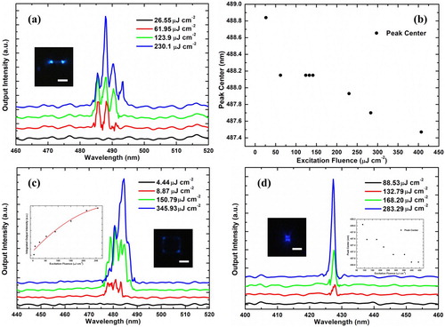
During in-plane self-assembly, not only NWs but also several microplates were obtained. We investigated the lasing properties of the microplates as well. The power-dependent emission spectra of the CsPbBrxCl3-x microplate with a size of 8.9 × 8.9 μm2 are shown in Figure (c); its lasing threshold was found to be 8.87 μJ·cm−2, which is indicated by the left inset. This value is much lower than those of the CsPbBr3 NWs, indicating the excellent crystallinity of the hybrid perovskites. The parallelogram shape of the microplate was confirmed by observation of its four shining edges (Figure (c), right inset); in this configuration, both F-P and gallery-whisper resonance modes can be excited. The multi-mode PL output of the microplate can become single-mode when its size is reduced, as seen, for example, for the 2.1 × 2.3 μm2 CsPbCl3 nanoplate in Figure (d). Here, too, a 1.15 nm blueshift is observed (Figure (d), inset).
Perovskites are sensitive to air, oxygen, water, temperature, and light irradiation [Citation13,Citation17,Citation18,Citation20,Citation21,Citation24,Citation29,Citation30]. Among these, light illumination can induce the severe photo-degradation of typical CsPbBr3 quantum dots [Citation8,Citation27]. Under ambient atmosphere (room temperature, 24 ± 1°C; and relative humidity, 30 ± 2%), we irradiated CsPbBr3, CsPbBrxCl3-x, and CsPbCl3 NWs with the pumping laser with 1.5, 3.0, and 3.3 Pth intensities, respectively, where Pth is the threshold of the NW, shown in Figure (a). All three samples retained over 90% lasing output compared to their initial states after 70 min. Compared with the reported results [Citation13,Citation20,Citation21,Citation24], we can demonstrate a much shorter pulse duration of 35–50 fs, which indicates higher peak power. Thus, our NWs may exhibit better durability.
Figure 5. (a) Stability of various perovskite CsPbX3 NW integrated emission intensities while exposed to ambient atmosphere. (b) Widely tuneable lasing emission wavelength from single-crystal NW of mixed cesium lead halide perovskites at room temperature and ambient atmosphere.
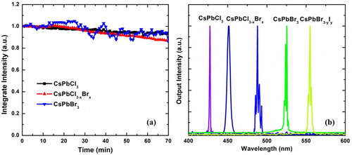
For other hybrid perovskite NWs, CsPbBrxCl3-x and CsPbBryI3-y, synthesised by in-plane self-assembly, similar lasing emission were also observed (Figure (b)). The threshold for an individual sample was tens of μJ cm−2 and the Q factor was a few hundred. NWs of CsPbBryI3-y can be grown by our method; their PL spectra are shown in Figure (f). Unfortunately, an efficient lasing wavelength above 560 nm could not be observed; the fluorescence gradually faded, regardless of the NWs were exposed to whether a mercury lamp or 400 nm laser pulse. To improve the photostability of the CsPbBryI3-y NWs synthesised by in-plane self-assembly, a further process such as annealing [Citation7], washing with methyl acetate [Citation31], a solution-processed secondary growth [Citation32], or incorporation of isovalent small ions [Citation33] is required.
4. Conclusions
In summary, inorganic cesium lead halide perovskite NWs were synthesised by an in-plane self-assembly method and their lasing performance was investigated in this work. The method is highly efficient, and the required material can be low to nanogram order. The NWs exhibit excellent single-crystal qualities and their photoluminescence range spanned 420–720 nm by stoichiometric tuning of the anions. The obtained NWs realised a lasing range of 420–560 nm, with typical threshold values for the CsPbBr3 NWs and CsPbBrxCl3-x nanoplates of 18.8 and 8.87 μJ cm−2, respectively. The NWs exhibited robust stability under high-power pulsed-laser irradiation in ambient atmosphere. Overall, the in-plane self-assembly method offers an efficient alternative approach for the exploration and development of cesium lead halide perovskite NWs for future nanophotonic applications.
Disclosure statement
No potential conflict of interest was reported by the authors.
ORCID
Additional information
Funding
References
- Jung HS, Park N-G. Perovskite solar cells: from materials to devices. Small. 2015;11:10–25. doi: 10.1002/smll.201402767
- Green MA, Ho-Baillie A, Snaith HJ. The emergence of perovskite solar cells. Nat Photon. 2014;8:506–514. doi: 10.1038/nphoton.2014.134
- Christians JA, Schulz P, Tinkham JS, et al. Tailored interfaces of unencapsulated perovskite solar cells for >1000 hour operational stability. Nat Energy. 2018;3:68–74. doi: 10.1038/s41560-017-0067-y
- Sutherland BR, Sargent EH. Perovskite photonic sources. Nat Photon. 2016;10:295–302. doi: 10.1038/nphoton.2016.62
- Zhang Q, Su R, Du W, et al. Advances in small perovskite-based lasers. Small Methods. 2017;1:1700163. doi: 10.1002/smtd.201700163
- Tang B, Dong H, Sun L, et al. Single-mode lasers based on cesium lead halide perovskite submicron spheres. ACS Nano. 2017;11:10681–10688. doi: 10.1021/acsnano.7b04496
- Egger DA, Bera A, Cahen D, et al. What remains unexplained about the properties of halide perovskites? Adv Mater. 2018;30:1800691. doi: 10.1002/adma.201800691
- Niu G, Guo X, Wang L. Review of recent progress in chemical stability of perovskite solar cells. J Mater Chem A. 2015;3:8970–8980. doi: 10.1039/C4TA04994B
- Zhang H, Wang X, Liao Q, et al. Embedding perovskite nanocrystals into a polymer matrix for tunable luminescence probes in cell imaging. Adv Funct Mater. 2017;27:1604382. doi: 10.1002/adfm.201604382
- Eaton SW, Fu A, Wong AB, et al. Semiconductor nanowire lasers. Nat Rev Mater. 2016;1:16028. doi: 10.1038/natrevmats.2016.28
- Ning C-Z, Dou L, Yang P-D. Bandgap engineering in semiconductor alloy nanomaterials with widely tunable bandgaps and compositions. Nat Rev Mater. 2017;2:17070. doi: 10.1038/natrevmats.2017.70
- Evans TJS, Schlaus A, Fu Y, et al. Continuous-wave lasing in cesium lead bromide perovskite nanowires. Adv Optical Mater. 2018;6:1700982. doi: 10.1002/adom.201700982
- Park K, Lee JW, Kim JD, et al. Light−matter interactions in cesium lead halide perovskite nanowire lasers. J Phys Chem Lett. 2016;7:3703–3710. doi: 10.1021/acs.jpclett.6b01821
- Zhou H, Yuan S, Wang X, et al. Vapor growth and tunable lasing of band gap engineered cesium lead halide perovskite micro/nanorods with triangular cross section. ACS Nano. 2017;11:1189–1195. doi: 10.1021/acsnano.6b07374
- Chen J, Fu Y, Samad L, et al. Vapor-phase epitaxial growth of aligned nanowire networks of cesium lead halide perovskites (CsPbX3, X = Cl, Br, I). Nano Lett. 2017;17:460–466. doi: 10.1021/acs.nanolett.6b04450
- Shoaib M, Zhang X, Wang X, et al. Directional growth of ultralong CsPbBr3 perovskite nanowires for high-performance Photodetectors. J Am Chem Soc. 2017;139:15592–15595. doi: 10.1021/jacs.7b08818
- Zhu H, Fu Y, Meng F, et al. Lead halide perovskite nanowire lasers with low lasing thresholds and high quality factors. Nat Mater. 2015;14:636–642. doi: 10.1038/nmat4271
- Fu Y, Zhu H, Schrader AW, et al. Nanowire lasers of formamidinium lead halide perovskites and their stabilized alloys with improved stability. Nano Lett. 2016;16:1000–1008. doi: 10.1021/acs.nanolett.5b04053
- Petrov AA, Pellet N, Seo J-Y, et al. New insight into the formation of hybrid perovskite nanowires via structure directing adducts. Chem Mater. 2017;29:587–594. doi: 10.1021/acs.chemmater.6b03965
- Eaton SW, Lai M-L, Gibson NA, et al. Lasing in robust cesium lead halide perovskite nanowires. Proc Natl Acad Sci USA. 2016;113:1993–1998. doi: 10.1073/pnas.1600789113
- Dou L, Lai M-L, Kley CS, et al. Spatially resolved multicolor CsPbX3 nanowire heterojunctions via anion exchange. Proc Natl Acad Sci USA. 2017;114:7216–7221. doi: 10.1073/pnas.1703860114
- Zhang D-D, Yang Y-M, Bekenstein Y, et al. Synthesis of composition tunable cesium lead halide nanowires through anion-exchange reactions. J Am Chem Soc. 2016;138:7236–7239. doi: 10.1021/jacs.6b03134
- Lai M, Kong Q, Bischak CG, et al. Structural, optical, and electrical properties of phasecontrolled cesium lead iodide nanowires. Nano Res. 2017;10:1107–1114. doi: 10.1007/s12274-016-1415-0
- Fu Y-P, Zhu H-M, Stoumpos CC, et al. Broad wavelength tunable robust lasing from single-crystal nanowires of cesium lead halide perovskites (CsPbX3, X = Cl, Br, I). ACS Nano. 2016;10:7963–7972. doi: 10.1021/acsnano.6b03916
- Protesescu L, Yakumin S, Bodnarchuk MI, et al. Nanocrystals of cesium lead halide perovskites (CsPbX3, X = Cl, Br, and I): novel optoelectronic materials showing bright emission with wide color gamut. Nano Lett. 2015;15:3692–3696. doi: 10.1021/nl5048779
- Nedelcu G, Protesescu L, Ykunin S, et al. Fast anion-exchange in highly luminescent nanocrystals of cesium lead halide perovskites (CsPbX3, X = Cl, Br, I). Nano Lett. 2015;15:5635–5640. doi: 10.1021/acs.nanolett.5b02404
- Tian T, Cai B, Sugihara O. DAST single-nanometer crystal preparation using a substrate-supported rapid evaporation crystallization method. Nanoscale. 2016;8:18882–18886. doi: 10.1039/C6NR07378F
- Li Y, Guan S, Liu Y, et al. Growth of cesium lead halide perovskite nanorods through a one-drop self-assembly and ion-exchange. Opt Express. 2018;26:33856–33864. doi: 10.1364/OE.26.033856
- Wang Y, Li X, Song J, et al. All-inorganic colloidal perovskite quantum dots: a new class of lasing materials with favorable characteristics. Adv Mater. 2015;27:7101–7108. doi: 10.1002/adma.201503573
- Chen J, Liu D, Al-Marri MJ, et al. Photo-stability of CsPbBr3 perovskite quantum dots for optoelectronic application. Sci China Mater. 2016;59:719–727. doi: 10.1007/s40843-016-5123-1
- Swarnkar A, Marshall AR, Sanehira EM, et al. Quantum dot–induced phase stabilization of α-CsPbI3 perovskite for high-efficiency photovoltaics. Science. 2016;354:92–95. doi: 10.1126/science.aag2700
- Luo D, Yang W, Wang Z, et al. Enhanced photovoltage for inverted planar heterojunction perovskite solar cells. Science. 2018;360:1442–1446. doi: 10.1126/science.aap9282
- Saidaminov MI, Kim J, Jain A, et al. Suppression of atomic vacancies via incorporation of isovalent small ions to increase the stability of halide perovskite solar cells in ambient air. Nat Energy. 2018;3:648–654. doi: 10.1038/s41560-018-0192-2