
Abstract
Epitaxial Cr2AlC MAX phase thin films were grown on MgO(111) and Al2O3(0001) by pulsed laser deposition (PLD) at 600°C. X-ray diffraction and morphology studies of Cr2AlC thin films on MgO (111) reveal phase purity, columnar growth, the epitaxial relation Cr2AlC(0001) || MgO(111) and Cr2AlC [11-20] || MgO[10-1] and similar growth behaviour on Al2O3(0001). Resistivity measurements show semiconductor-like behaviour for 10 and 20 nm thick films, and metallic-like behaviour for thicker films, suggesting a percolation thickness slightly above 20 nm. Our results demonstrate the potential of PLD as a novel method for the growth of epitaxial MAX phase thin films.
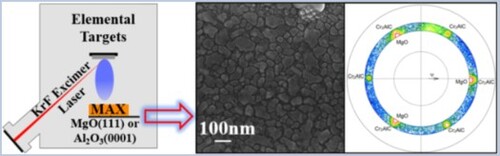
GRAPHICAL ABSTRACT
IMPACT STATEMENT
Pulsed Laser Deposition is applied to grow phase pure and epitaxial Cr2AlC MAX phase thin films on MgO(111) and Al2O3(0001). Control of the sample stoichiometry is achieved by elemental targets.
Introduction
Transition metal carbides and nitrides constitute a large family of compounds with layered hexagonal structures and chemical formula Mn+1AXn (n = 1 … 3), where M is an early transition metal from the 3d, 4d or 5d series, A is a main-group element and X stands for C or N [Citation1]. MAX phases are well-known for their unique combination of metallic and ceramic properties [Citation1,Citation2]. Like metals, they are readily machinable, ductile, electrically and thermally conductive [Citation3]. Like ceramics, MAX phases are thermal-shock resistant and refractory, thus they possess superior mechanical characteristics and chemical stability. In addition, magnetic properties have been theoretically predicted and experimentally demonstrated for Cr- and Mn-based MAX phases, their solid solutions and recently discovered in-plane ordered i-MAX phases [Citation4–7]. MAX phases can show different kinds of magnetism ranging from paramagnetic to ferromagnetic and antiferromagnetic states (including incommensurate spin structures and competing interactions) depending on their elemental composition, synthesis parameters and temperature [Citation4,Citation7,Citation8].
Studies of MAX phases have been performed on single crystals [Citation9,Citation10], bulk materials [Citation11,Citation12], powders [Citation13] and thin films [Citation4,Citation14–16]. However, bulk materials and powders are usually polycrystalline with traces of secondary phases [Citation17,Citation18]. These affect the electric and magnetic properties and often hinder a profound interpretation of data. On the contrary, single crystals and epitaxial single-phase thin films are ideal model systems to explore the intrinsic properties of MAX phases and their anisotropies [Citation6,Citation19].
Several physical deposition techniques have been considered for the growth of epitaxial MAX phase thin films, among which magnetron sputtering and cathodic arc deposition are most common [Citation4,Citation20]. In addition, phase-pure polycrystalline Cr2AlC films have been successfully deposited using high power impulse magnetron sputtering [Citation21]. Besides these techniques, pulsed laser deposition (PLD) is a well-established tool to grow epitaxial films [Citation22–24]. PLD allows the stabilization of metastable phases [Citation22,Citation24] and gives rise to a good mixture of deposited elements. Moreover, the stoichiometry can be precisely adjusted using elemental targets, and it is only limited by the amount of material deposited per laser pulse (about 0.01 monolayer). Several attempts of growing epitaxial MAX phase thin films by PLD failed in the past due to the non-stoichiometric transfer of atoms from target to the film and the crystallization of unwanted side phases [Citation25–31]. To date, there is only one report on the growth of MAX phases by PLD, yielding (103) oriented nanolaminate Ti3AlC2 films deposited on Al2O3(0001) substrates [Citation32].
In this work, we present the first successful preparation of epitaxial single-phase Cr2AlC MAX phase thin films on MgO(111) and Al2O3(0001) substrates by PLD at 600°C with various thicknesses ranging from 10 nm to 50 nm. Structure, morphology and electrical resistivity are investigated as function of film thickness. A columnar growth with the epitaxial relation Cr2AlC(0001) || MgO(111) and Cr2AlC [11-20] || MgO[10-1] is identified. On Al2O3(0001), the c-axis orientation is identical, the in-plane growth direction, however, cannot be unambiguously determined due to overlapping film and substrates peaks in XRD pole figures.
The epitaxial Cr2AlC films have been suggested as a parent compound for the formation of quaternary MAX phases by doping magnetic elements from the 3d series, such as Fe or Mn promoting long-range magnetic order [Citation4].
Materials and methods
The growth of Cr2AlC MAX phase thin films was carried out in ultra-high vacuum (base pressure < 1·10−8 mbar) by PLD [Citation21]. An KrF Excimer Laser (wavelength 248 nm) hits pure elemental targets of chromium (Cr, 99,95%), aluminium (Al, 99,99%) and pyrolytic graphite (C, 99,999%) purchased from Kurt J. Lesker (USA) at an energy density of 13 J·cm−2. The MAX phase thin films were grown by sequential layer by layer deposition corresponding to a ratio of 2:5:1 for Cr, Al, and C, respectively, on MgO(111) and Al2O3(0001) substrates at a substrate temperature of 600°C. The amount of aluminium was set five times higher as compared to the stoichiometric value due to (i) the tendency of Al droplet formation; (ii) the high substrate temperature resulting in thermal desorption of Al [Citation33] and (iii) re-sputtering effects of lighter elements during deposition. A similar approach has been used in the preparation of epitaxial FeAl films on Al2O3 [Citation24]. The deposition rate was monitored using a quartz crystal.
Structural characterization of the thin films was performed by X-ray Diffraction (XRD) in Bragg–Brentano geometry using a Panalytical X’Pert MPD PW3040 and an Empyrean MRD device using Cu-Kα radiation (λ = 1.5406 Å). The in-plane epitaxial relation between substrate and MAX phase was determined by pole figures.
The surface morphology was studied using Scanning Electron Microscopy (SEM) and Atomic Force Microscopy (AFM), employing Zeiss LEO 1530 and Park Systems XE70 microscopes, respectively. Surface roughness measurements by AFM were performed in noncontact mode using an ACTA10M type cantilever with a tip radius of 6 nm. The roughness was determined for individual islands in a scan area of 1 µm × 1 µm using the software WSxM 5.0 Develop 9.1.
Resistivity measurements were performed in four-point geometry using a custom-built sample holder in a PPMS DynaCool system. The spring-tip contacts were pressed onto the film surface and fixed. The distance between contacts was 2 mm.
Results and discussions
10–50 nm Cr2AlC thin films were grown on MgO(111) and Al2O3(0001) substrates at 600°C. All films are metallic-grey with decreasing transparency for increasing thickness—as expected. The film stoichiometry was optimized prior to deposition of the epitaxial films. The film thickness is adjusted by the number of repetitions of the Cr–Al–Cr–C sequence, the deposition rate has been determined for each elemental target individually and the number of laser pulses per target was optimized for one monolayer per element.
Figure (a) shows the X-ray diffractograms of Cr2AlC films grown on MgO(111) substrates at 600°C for various film thicknesses. The films are single phase and highly textured showing sharp peaks originating only from (0001) planes of Cr2AlC, beside substrate peaks. To further examine the film texture, XRD pole figure measurements of the (10-13) Cr2AlC MAX phase diffraction peaks were performed as presented in Figure (b). The pole figure displays three intense peaks of elongated circular shape originating from (110) plane of the MgO substrate. Three of the six Cr2AlC (10-13) MAX phase diffraction peaks are positioned at identical in-plane angles φ, but at different ψ as seen by the shoulders towards larger ψ angles. The MAX phase peaks show the expected 6-fold symmetry of a hexagonal lattice. Thus, XRD confirms epitaxy of Cr2AlC(0001) || MgO(111) and in-plane Cr2AlC[11-20] || MgO[10-1].
Figure 1. (a) XRD θ–2θ scans of Cr2AlC films on MgO(111) for various thicknesses. Substrate peaks are marked by ‘S’. Sticks and Miller indices reflect the angular position and intensity of Cr2AlC powder (ICDD 01089-2275). (b) Pole figure on the (10-13) diffraction peak at 2θ = 42.08° of the 20 nm film.
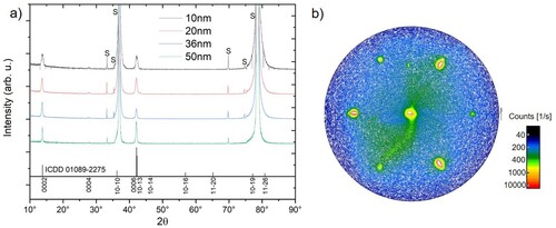
The c-lattice parameter calculated from θ to 2θ scans and a-lattice parameter calculated from pole figure measurements [Citation34] (see Table ) are in agreement with the lattice parameter for bulk Cr2AlC (a = 0.286 nm and c = 1.282 nm) [Citation4]. Remarkably, the lattice parameters are independent of the film thickness. The a-lattice parameter has larger uncertainties due to the larger ψ step size in the pole figures. The coherence length has been calculated from Scherrer’s formula [Citation35], resembling the film thickness for 10 and 20 nm films. The surface morphology is investigated by SEM (Figure ) and AFM. From the latter we determined the root mean square (RMS) roughness of the Cr2AlC islands grown on the MgO(111) substrate (Table ).
Figure 2. Top view SEM images of Cr2AlC thin films on MgO(111) deposited at 600°C for different thicknesses.
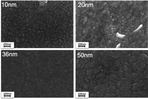
Table 1. Lattice parameters and XRD coherence length of Cr2AlC films grown on MgO(111) and Al2O3(0001) substrates, root-mean-square (RMS) surface roughness of the Cr2AlC grains and resistivity values at T = 300 K. The temperature characteristics of the resistivity is indicated by semiconductor-like ‘SC’ or metallic ‘M’.
The SEM images in Figure reveal the morphology of the grown films. Well-resolved islands of irregular shape are obtained for all thicknesses. The lateral island size grows with increasing film thickness. Islands of the 10 nm thick film are rather small and flat (laterally 185 ± 82 nm) and well separated from each other proving a columnar growth mode. The grains are not percolated suggesting the existence of no or weak bottleneck-like connections between them (Figure (a)). With increasing film thickness the island size gradually increases up to 330 ± 135 nm for the 50 nm film. In comparison, rf-magnetron sputtering delivers films at about 100 nm lateral grain size on MgO(100) substrate [Citation20]. With increasing thickness, the percolation limit is reached for thicknesses in between 20 and 36 nm. We address this below in the discussion of the resistivity. For thicker films, the initial islands percolate and overall result in a Volmer-Weber growth continuation [Citation36]. The RMS roughness (Table ) of the grains is 0.7 ± 0.2 nm for the 10 nm film. For thicker films (20 and 36 nm), the islands become smoother with RMS values of 0.64 and 0.43 nm. Due to the island growth, the RMS roughness over the entire film is about 4 nm and thus considerably larger as compared to the roughness of the individual island surfaces. We conclude that PLD yields high-quality epitaxial films.
As a first step towards applications, we investigated the electrical transport properties. The temperature dependence of the electrical resistivity of the 20 and 36 nm Cr2AlC films on MgO(111) are shown in Figure (a,b). Interestingly, the characteristics of the resistivity is highly thickness dependent, showing a semiconductor-like behaviour for the 20 nm Cr2AlC film in comparison with the expected metallic behaviour for the 36 nm film. Note that the resistivity of the 20 nm film is 104 times larger as compared to the 36 nm film. While for the 10 nm film the absolute resistance exceeds 10 GΩ, the 50 nm film shows similar metallic characteristics as the 36 nm film (Table ). We ascribe this puzzling change from semiconductor-like to metallic characteristics to the film morphology, since the flat islands coalesce between 20 and 36 nm. Each Cr2AlC MAX phase island is assumed to have metallic conductivity in the film plane, however, charge carriers must jump (e.g. by hopping or tunnelling) from island to island before good contacts between islands are achieved for thicker films. Cr2AlC MAX phase films slightly below the percolation may be used in the future as ultra-sensitive and fast humidity sensors, presumably better than their MXene counterparts since the absolute resistance and thus the achievable contrast is higher and adjustable [Citation37].
Figure 3. Temperature dependence of the resistivity for Cr2AlC thin films deposited on MgO(111) and Al2O3(0001) substrates.
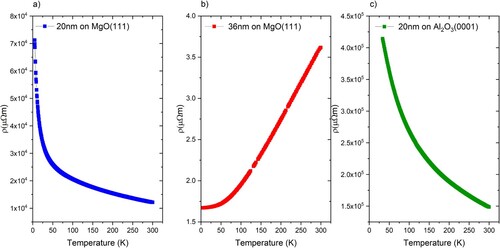
Quantitatively, the resistivity decreases as the temperature is reduced from 300 to 2 K for 36 nm Cr2AlC film. In this case, the electrical resistivity values are 1.7 µΩm and 3.6 µΩm at 2 K and 300 K, respectively. The latter is higher than the reported resistivity for bulk Cr2AlC MAX phases (0.60–0.74 µΩm) [Citation38–40] and the resulting residual resistance ratio (RRR) of 2.17 is rather low. We ascribe this to a more pronounced surface scattering in the films. Note that for Cr2AlC thin films produced by other deposition techniques similar resistivity values were reported [Citation41,Citation42].
Using identical deposition conditions, we have simultaneously grown a Cr2AlC thin films on Al2O3(0001). Although the lattice mismatch between Cr2AlC and Al2O3(0001) is ∼ −4.0% while between Cr2AlC and MgO(111) is ∼ +4.0%, growth of textured films is possible on both substrates. The structural and morphological characteristics of the 20 nm film on Al2O3(0001) are presented in Figure .
Figure 4. (a) XRD θ–2θ scans for 20 nm Cr2AlC MAX phase films deposited on Al2O3(0001) and MgO(111) substrates at 600°C. Substrate peaks are marked by ‘S’. The inset presents the (10-13) pole figure. (b) Top view SEM image of the 20 nm film. (c, d) AFM images of the 20 nm thick Cr2AlC films on MgO(111) and Al2O3(0001) substrates.
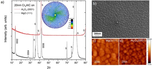
The Cr2AlC film on Al2O3(0001) only displays (0001) peaks originating from the Cr2AlC MAX phase besides the strong substrate diffraction peaks proving the formation of a single phase Cr2AlC (see Table ). However, the in-plane epitaxial relationship of Cr2AlC films on Al2O3(0001) is difficult to prove due to overlapping substrate peaks. The corresponding pole figure shows six intense peaks (Figure (a), inset), which originate from the {11-23} planes in sapphire crystal lattice. The rather weak intensity of (10-13) XRD peaks from the Cr2AlC film is lost within the high intensity of the substrate peaks. Since we do not detect any hints of a ring-shaped diffraction intensity in the pole figure which would indicate textured growth with no regular in plane orientation of grains, we assume that the Cr2AlC thin film grows epitaxially on Al2O3(0001).
SEM and AFM surface morphologies of the deposited films are shown in Figure (b–d). It can be seen in Figure (b) that the 20 nm Cr2AlC film on Al2O3(0001) has smaller grains (175 ± 87 nm) as compared to the 20 nm film deposited on MgO(111) substrate (280 ± 165 nm). This is expected considering the plane misfits – resulting in more dislocations – between the MAX phase layer and the Al2O3 substrate [Citation43]. As shown in Figure (c), the 20 nm thick Cr2AlC film on Al2O3(0001) substrate shows a similar semiconductor-like resistivity as the 20 nm film deposited on MgO(111).
Conclusion
We have shown that PLD can be used to grow high-quality epitaxial Cr2AlC thin films on MgO(111) and Al2O3(0001) substrates at 600°C. It is essential to use elemental targets, since the individual elemental deposition must be tuned precisely to the targeted stoichiometry. In Cr2AlC MAX phase thin films we find bulk-like a- and c-lattice parameters independent of the film thickness ranging from 10 nm to 50 nm. Epitaxial films are obtained with Cr2AlC(0001) || MgO (111) and Cr2AlC [11-20] || MgO[10-1], grown in a columnar growth mode. On Al2O3(0001), the orientation is most likely similar, but due to overlapping substrate peaks in pole figures we cannot unambiguously prove this. Resistivity measurements reveal a percolation thickness slightly above 20 nm. A semiconductor-like temperature dependent resistivity is measured for the 10 and 20 nm films while after percolation the resistivity shows the expected metallic temperature dependence.
Acknowledgements
The authors thank Detlef Spoddig for assistance with SEM and EDX imaging. Michael Vennemann is acknowledged for the help and training in XRD. We thank Merlin Schmuck and Doru Lupascu for assistance and providing access to the XRD with Eulerian cradle. We also thank Soma Salamon and Ulrich von Hörsten for their support in the optimization of the deposition chamber.
Disclosure statement
No potential conflict of interest was reported by the author(s).
Data availability statement
The data supporting the findings of this study are available from the corresponding author upon reasonable request.
Additional information
Funding
References
- Barsoum MW. The M(x+1)AX(x) phases: a new class of solids; thermodynamically stable nanolaminates. Prog Solid State Chem. 2000;28:201–281.
- Högberg H, Hultman L, Emmerlich J, et al. Growth and characterization of MAX-phase thin films. Surf Coat Technol. 2005;193(1–3):6–10.
- Eklund P, Rosen J, Persson PO. Layered ternary Mn+1AXn phases and their 2D derivative MXene: an overview from a thin-film perspective. J Phys D Appl Phys. 2017;50:113001.
- Ingason AS, Dahlqvist M, Rosen J. Magnetic MAX phases from theory and experiments; a review. J Phys-Condens Mater. 2016;28(43):433003.
- Sun ZM. Progress in research and development on MAX phases: a family of layered ternary compounds. Int Mater Rev. 2013;56(3):143–166.
- Salikhov R, Semisalova AS, Petruhins A, et al. Magnetic anisotropy in the (Cr0.5Mn0.5)2GaC MAX phase. Mater Res Lett. 2015;3(3):156–160.
- Novoselova IP, Petruhins A, Wiedwald U, et al. Large uniaxial magnetostriction with sign inversion at the first order phase transition in the nanolaminated Mn2GaC MAX phase. Sci Rep. 2018;8:2637.
- Dahlqvist M, Rosen J. Impact of strain, pressure, and electron correlation on magnetism and crystal structure of Mn2GaC from first-principles. Sci Rep. 2020;10(1):11384.
- Ito T, Pinek D, Fujita T, et al. Electronic structure of Cr2AlC as observed by angle-resolved photoemission spectroscopy. Phys Rev B. 2017;96(19):195168.
- Badr HO, Champagne A, Ouisse T, et al. Elastic properties and hardness values of V2AlC and Cr2AlC single crystals. Phys Rev Mater. 2020;4(8):083605.
- Scabarozi TH, Amini S, Finkel P, et al. Electrical, thermal, and elastic properties of the MAX-phase Ti2SC. J Appl Phys. 2008;104(3):033502.
- Tian W, Wang P, Zhang G, et al. Synthesis and thermal and electrical properties of bulk Cr2AlC. Scr Mater. 2006;54(5):841–846.
- Siebert JP, Bischoff L, Lepple M, et al. Sol–gel based synthesis and enhanced processability of MAX phase Cr2GaC. J Mater Chem C. 2019;7(20):6034–6040.
- Ingason AS, Petruhins A, Rosen J. Toward structural optimization of MAX phases as epitaxial thin films. Mater Res Lett. 2016;4(3):152–160.
- Högberg H, Eklund P, Emmerlich J, et al. Epitaxial Ti2GeC, Ti3GeC2, and Ti4GeC3 MAX-phase thin films grown by magnetron sputtering. J Mater Res. 2005;20(4):779–782.
- Tao Q, Salikhov R, Mockute A, et al. Thin film synthesis and characterization of a chemically ordered magnetic nanolaminate (V,Mn)3GaC2. APL Mater. 2016;4(8):086109.
- Sobolev KV, Kolincio KK, Emelyanov A, et al. Evolution of magnetic and transport properties in (Cr1-xMnx)2AlC MAX-phase synthesized by arc melting technique. J Magn Magn Mater; 493:165642.
- Hamm CM, Duerrschnabel M, Molina-Luna L, et al. Structural, magnetic and electrical transport properties of non-conventionally prepared MAX phases V2AlC and (V/Mn)2AlC. Mater Chem Front. 2018;2(3):483–490.
- Salikhov R, Meshkian R, Weller D, et al. Magnetic properties of nanolaminated (Mo0.5Mn0.5)2GaC MAX phase. J Appl Phys. 2017;121(16):163904.
- Su R, Zhang H, Meng X, et al. Synthesis of Cr2AlC thin films by reactive magnetron sputtering. Fusion Eng Des. 2017;125:562–566.
- Qureshi MW, Ma X, Tang G, et al. Fabrication and mechanical properties of Cr2AlC MAX phase coatings on TiBw/Ti6Al4V composite prepared by HiPIMS. Mater. 2021;14(4):826.
- Eason R. Pulsed laser deposition of thin films: applications-Led growth of functional materials. Hoboken (NJ): Wiley; 2007.
- Trautvetter M, Wiedwald U, Paul H, et al. Thermally driven solid-phase epitaxy of laser-ablated amorphous AlFe films on (0001)-oriented sapphire single crystals. Appl Phys A. 2011;102(3):725–730.
- Yao X, Wiedwald U, Trautvetter M, et al. Growth modes and epitaxy of FeAl thin films on a-cut sapphire prepared by pulsed laser and ion beam assisted deposition. J Appl Phys. 2014;115(2):023507.
- Lange C. Construction of a pulsed laser deposition (PLD) system and investigations on PLD in the MAX phase systems Ti-Si-C, Cr-Al-C and Ti-Al-N [dissertation]. Göttingen: Georg-August-University at Göttingen; 2009. German.
- Lange C, Barsoum MW, Schaaf P. Towards the synthesis of MAX-phase functional coatings by pulsed laser deposition. Appl Surf Sci. 2007;254(4):1232–1235.
- Lange C, Hopfeld M, Wilke M, et al. Pulsed laser deposition from a pre-synthesized Cr2AlC MAX phase target with and without ion-beam assistance. Phys Status Solidi A. 2012;209(3):545–552.
- Phani AR, Krzanowski JE. Structural and mechanical properties of TiC and Ti-Si-C films deposited by pulsed laser deposition. J Vac Sci Technol A. 2001;19:2252.
- Eklund P, Palmquist JP, Wilhelmsson O. et al. Comment on “Pulsed laser deposition and properties of Mn+1AXx phase formulated Ti3SiC2 thin films”. Tribol Lett. 2014;17:977–978.
- Hu JJ, Zabinski JS. Reply to the comment on “Pulsed laser deposition and properties of M n+1AX n phase formulated Ti3SiC2 thin films”. Tribol Lett. 2004;17:979–982.
- Hu J, Bultman J, Patton S, et al. Pulsed laser deposition and properties of Mn+1AXn phase formulated Ti3SiC2 thin films. Tribol Lett. 2004;16:113–122.
- Biswas A, Sengupta A, Rajput U, et al. Growth, properties, and applications of pulsed laser deposited nanolaminate Ti3AlC2 thin films. Phys Rev Appl. 2020;13(4):044075.
- Rues H, Mto B, Mraz S, et al. HPPMS deposition from composite targets: effect of two orders of magnitude target power density changes on the composition of sputtered Cr-Al-C thin film. Vacuum. 2017;145:285–289.
- Hogan DW, Dyson DJ. Angles between planes in the hexagonal and tetragonal crystal systems. Micron. 1970;2:59–61.
- Patterson AL. The Scherrer formula for X-Ray particle size determination. Phys Rev. 1939;56(10):978–982.
- Volmer M, Weber A. Nucleation in supersaturated formations. Z Phys Chem. 1926;119U(1):277–301. German.
- Römer FM, Wiedwald U, Strusch T, et al. Controlling the conductivity of Ti3C2 MXenes by inductively coupled oxygen and hydrogen plasma treatment and humidity. RSC Adv. 2017;7(22):13097–13103.
- Ying G, He X, Li M, et al. Effect of Cr7C3 on the mechanical, thermal, and electrical properties of Cr2AlC. J Alloys Compd. 2011;509(31):8022–8027.
- Hettinger JD, Lofland SE, Finkel P, et al. Electrical transport, thermal transport, and elastic properties of M2AlC(M = Ti,Cr,Nb, and V). Phys Rev B. 2005;72(11).
- Zhou WB, Mei BC, Zhu JQ. On the synthesis and properties of bulk ternary Cr2AlC ceramics. Mater Sci-Poland. 2009;24(4):973–980.
- Field MR, Carlsson P, Eklund P, et al. A combinatorial comparison of DC and high power impulse magnetron sputtered Cr2AlC. Surf Coat Technol. 2014;259:746–750.
- Stelzer B, Chen X, Bliem P, et al. Remote tracking of phase changes in Cr2AlC thin films by In-situ resistivity measurements. Sci Rep. 2019;9(1):8266.
- Naragan J, Larson BC. Domain epitaxy: a unified paradigm for thin film growth. J Appl Phys. 2003;93(1):278.