
 ?Mathematical formulae have been encoded as MathML and are displayed in this HTML version using MathJax in order to improve their display. Uncheck the box to turn MathJax off. This feature requires Javascript. Click on a formula to zoom.
Abstract
Here, a WS2-based photodetector is fabricated and its detection range is extended to optical communication waveband by pressure. At ambient pressure, WS2 exhibits a fast photoelectric response speed (rising/decaying time: 35/49 μs) under 635 nm laser illumination. Upon compression, the responsiveness and external quantum efficiency increase by two orders of magnitude under NIR illumination with different wavelengths as the pressure increases up to 17.2 GPa. The pressure-induced band gap reduction is mainly ascribed to the enhanced S-S interlayer interaction, leading to significant enhancement in the WS2 photoresponsiveness. This study paves the way for designing high-performance broadband photodetectors through pressure modification.
IMPACT STATEMENT
Fast photoelectric response speed and extended detection range were achieved in the WS2-based photodetector via pressure modulation, which paves a new way for designing high-performance broadband photodetectors.
GRAPHICAL ABSTRACT

Introduction
High-performance infrared photodetectors have attracted widespread attention owing to their wide applications in industrial and scientific fields [Citation1–5]. Layered materials, such as graphene and black phosphorus, are often used as promising infrared photodetectors, presenting novel physical properties and excellent optoelectronic properties. However, with the ever-increasing demands, the disadvantages of the zero bandgap in graphene and the environmental instability in black phosphorus limit their further development in infrared photoelectric detection technology [Citation6–8]. Therefore, there is an urgent requirement for novel infrared detection materials and feasible methods for the improvement of the detection performance of photoelectric materials in the infrared waveband.
Recently, transition metal dichalcogenides (TMDs) have attracted extensive attention in the scientific community [Citation9–12]. TMDs exhibit various outstanding physical properties such as tunable band gap, high optical absorption, and strong spin–orbit coupling that have immense potential in the fields of energy, catalysis, and optoelectronics [Citation13–19]. TMDs have a typical sandwiched structure. The middle layer consists of transition metal atoms, and the top and bottom layers are made of chalcogen atoms. The intralayer atoms are covalently bonded, while the interlayers are connected by van der Waals forces [Citation20]. Therefore, they can be easily exfoliated into multilayers or even monolayer nanosheets via ultrasonic or mechanical methods [Citation21–24]. Similar to the most well-known TMDs, 2H-WS2 is a widely studied TMD with thickness-dependent indirect-direct bandgap transitions and various bandgap values [Citation25–27], for its individual use as a substrate material for photodetectors, the performance-tuning methods for WS2-based photodetectors often focus on improving the quality of the prepared WS2 and tuning its number of layers. Substantial efforts have been devoted to improving the WS2 photoelectronic properties since Perea-Lopez et al. [Citation28] first used it in the preparation of photodetectors, increasing its responsiveness, response time, and response range to 53.3 A W−1, 560 μs, and 1064 nm, respectively [Citation29–33]. This series of studies provide new prospects for enhancing the photoelectronic properties of WS2. However, improving the photoelectric properties of WS2 devices further with faster response speeds and wider spectral response ranges is still an enormous challenge.
Employment of high pressure is an effective method of modulating the bandgap and electronic states of materials that can further tune photoelectronic-related properties. Unlike chemical doping and molecular modifications [Citation34,Citation35], the application of pressure does not introduce chemical impurities and is more controllable. Recently, pressure-induced enhancement of photoelectric properties has been realized in a variety of materials, such as perovskites, Bi2O2S, AgIn5S8, and iodine [Citation36–40]. In TMDs, enhanced photoelectric properties have been observed in ReS2 and PtS2 under pressure [Citation41,Citation42]. 2H-WS2 has excellent mobility and carrier density than PtS2 and ReS2, which shows the advantages in photoelectric applications [Citation43–48]. Previous experimental and theoretical calculation results have revealed that the applied pressure not only effectively regulates the charge carrier characteristics of WS2 but also substantially modulates the light absorption ability of WS2 [Citation47,Citation49]. All these properties are inextricably linked to the photoelectronic properties of a semiconductor, and therefore, it is anticipated that pressure regulation may be an effective method of modifying the photoelectric performance of WS2.
In this study, we systematically investigate the photoelectric properties of WS2 under pressure. The WS2-based photodetector prepared in a pressure cell simultaneously achieves an ultra-fast response speed and a broad detection range at ambient pressure. The photoelectrical properties of WS2 are significantly enhanced under high-pressure modulation in the detection range from visible to NIR. The continuous tuning of the photoelectric properties provides a platform for developing pressure-modulated devices for future functional material technologies.
Materials and methods
Sample characterization
WS2 crystal was purchased from 6Carbon Technology (Shenzhen, China). The sample was characterized by X-Ray diffraction (XRD, Rigaku Synergy Custom FR-X) with Mo Kα radiation (λ = 0.7099 Å) and scanning electron microscopy (SEM, FEI Magellan 400). A JEOL (JEM-2200FS) instrument with an accelerating voltage of 200 kV was employed for high-resolution transmission electron microscopy (HRTEM) and selected area electron diffraction (SAED).
In-situ XRD and Raman measurements
High pressure was generated using a diamond anvil cell (DAC) with a pair of diamond anvils (300 µm culet). Pressure was measured via the ruby fluorescence method. Silicone oil was used as the pressure-transmitting medium in the experiments. In-situ high-pressure XRD was measured by Rigaku Synergy Custom FR-X. The Raman spectra were recorded using a Renishaw inVia notch filter spectrometer equipped with a 514.5 nm exciting laser.
Photocurrent
In-situ high-pressure photocurrent measurements were conducted in a symmetrical DAC with a pair of diamonds with a culet size of 400 μm. A T301 stainless steel gasket was pre-indented to ∼50 μm (thickness), and a sample chamber with a diameter of ∼380 μm was drilled at the center of the indentation by a laser. An epoxy–boron nitride layer was inserted between the steel gasket and the diamond culet to achieve electrical insulation between the electrical leads and the metal gasket. Two platinum sheets were arranged to contact the sample in the chamber for photocurrent measurements as electrodes. The sample area between the two electrodes was approximately 8 × 10⁻⁹ m2. No pressure-transmitting medium was used for the photocurrent measurements. The photocurrents under pressure were recorded using a Keithley 2461 semiconductor characterization system under the illumination of a xenon lamp. A high-precision photocurrent scanning test microscope system (MStarter 200) with a source meter (Keithley 6482) was used for laser illumination of different wavelengths, including 635, 980 nm (power density: 15.3 mW cm−2), 1270 nm (power density: 5.7 mW cm−2), 1450 nm (power density: 5.4 mW cm−2) and 1650 nm (power density: 8.3 mW cm−2), the light power density under different wavelengths were measured by an optical power meter, the dark environment was required to avoid the interference of environmental light.
Computational details
All DFT calculations were performed using the projector augmented wave method (PAW) as implemented in the Vienna ab initio simulation package (VASP). The Perdew−Burke−Ernzerhof (PBE) was treated as the exchange–correlation potential within the generalized gradient approximation (GGA). We calculated the lattice parameters using the optB88b-vdW functional under pressure. The band gap and optical properties of WS2 under pressure were postprocessed using VASPKIT. The cut-off energy for the plane-wave was determined to be 600 eV, and Monkhorst−Pack k-point meshes spanning not more than 0.03 Å−3 in the Brillouin zone were chosen. The convergence for energy was set to 10−6 eV on each atom, and the internal atomic positions and lattice constants under each hydrostatic pressure were optimized until the force on each atom was less than 0.01 eV Å−1.
Results and discussion
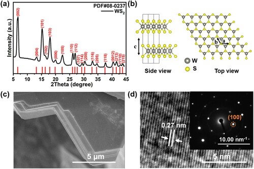
The XRD pattern of layered WS2 at ambient pressure is shown in Figure (a) which indicates that our sample has a 2H structure with space group P63/mmc, and its structure is schematically represented in Figure (b). Moreover, SEM and HRTEM measurements were obtained to investigate the crystal structure of WS2, and the results are displayed in Figure (c,d). These images clearly illustrate the layered stacking structure with a lattice spacing of 0.27 nm in WS2, and the corresponding SAED pattern (inset of Figure (d)) proves its hexagonal structure.
Figure 1. Sample characterization of 2H-WS2. (a) XRD pattern of WS2 at ambient pressure, the vertical lines at the bottom represent the theoretical diffraction peaks of 2H phase (space group P63/mmc). (b) Schematic of 2H-WS2 along the c-axis (left) and the ab plane (right), respectively. (c) The SEM image of WS2 indicates its layered structure. (d) HRTEM image of WS2, the inset SAED image shows the hexagonal structure of WS2.
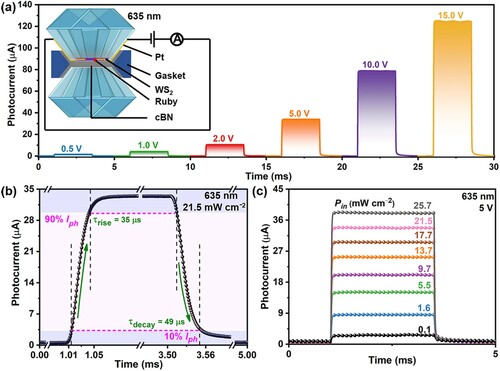
To evaluate the photoresponse performance of WS2, a series of optoelectronic measurements was performed within the DAC device using a two-point probe. The inset image of Figure (a) shows a schematic of the prepared installation. The relationship between the photocurrents and different biases with the light on/off time interval of 5 × 10⁻³ s is shown in Figure (a). In addition, the response speed is an important parameter to describe the quality of a photodetector, the rise time τrise (and decay time τdecay) is defined as the time intervals for the response rising (falling) from 10% (90%) to 90% (10%) of its peak value. As shown in Figure (b), under 635 nm laser illumination, τrise and τdecay are calculated as ∼35 μs and ∼49 μs, respectively, at ambient pressure. Compared with the previously reported WS2 photodetectors [Citation28–33,Citation50–55], our measured response and recovery times are the most rapid (Table S1). In addition, the effect of the illumination intensity (Pin) on the photoelectronic properties of WS2 was also studied. Figure (c) plots the photocurrents of WS2 under different Pin ranging from 0.1 to 25.7 mW cm−2 under 5 V bias. It is clearly observed that the photocurrents increase with increasing Pin, which could be understood that more photogenic electron–hole pairs contribute to the photocurrent due to the higher illumination intensity [Citation56]. Figure S1 displays the sublinear relationship between the photocurrent and Pin extracted from Figure (c), this phenomenon has been observed in several photoconductive detectors and is considered to be the result of electron–hole generation, trapping, and recombination in semiconductors [Citation4,Citation57–59].
Figure 2. (a) Photocurrents of WS2 photoelectrical devices dependent on different biases under ambient pressure. The inset is the schematic of our photocurrent measurements. (b) τrise and τdecay of WS2 under 635 nm laser illumination at 5 V bias. (c) Photocurrents of WS2 under different Pin.
The effects of pressure on the photoresponsiveness of WS2 were further investigated. Figure (a) displays the photocurrents of WS2 device under xenon lamp irradiation (Pin = 1.2 mW cm−2) at selected pressures with 5 V bias, and the observed linear I–V curves demonstrate that there is good Ohmic contact between WS2 and electrodes, as shown in Figure S2a. The responsivity (R)
(1)
(1) is described as the photocurrent generated per unit power of the incident light on the effective area, that is, Iph = Iillumination − Idark, S is the effective illuminated area [Citation60,Citation61]. During the compression process, the increase photoelectric response time of WS2 is mainly owing to enhanced interatomic interaction, as shown in Figure S2b [Citation62]. In addition, the effect of pressure on the WS2 optoelectronic properties can be expressed by the dependence of the photocurrent and R on the pressure, as presented in Figure (b). The value of R reaches ∼692.9 A W−1 at 20.1 GPa that is ∼20 times that at 1.4 GPa (35.6 A W−1). In addition, according to the given formula, when Pin and S remain constant, as the pressure increases, ∼20-fold increase in the photocurrent of the WS2 device is achieved by pressure tuning. However, the absence of a significant increase in specific detectivity is considered mainly due to the inevitable increase in dark current with the applied pressure, as shown in Figure S2c and d. However, compared to the previous literatures, the specific detectivity under high pressure remains basically stable at a relatively high order of 1011 [Citation29–32,Citation50,Citation51], as shown in Table S1. The pressure-induced photocurrent increase is closely related to the decrease of bandgap, which is calculated in the following theoretical section. As the band gap decreases, electrons in the conduction band are more likely to be excited into the conduction band by the same illuminated wavelength. This phenomenon has also been observed in other single-crystal TMDs, such as PtS2 and ReS2, however, the photocurrent enhancement of WS2 is much higher than the previous reports [Citation41,Citation42].
Figure 3. (a) Photocurrents at selected pressures of WS2 under xenon lamp irradiation. (b) Pressure-dependent photocurrents (left axis) and responsivity (right axis) under xenon lamp irradiation during compression. (c–d) Photocurrents of WS2 under the illumination wavelength of 980 nm and 1650 nm at selected pressures. (e) Photocurrent–pressure dependence of layered WS2 with 980, 1270, 1450, and 1650 nm NIR wavelengths. (f) R and EQE of WS2 as a function of pressure under illumination of selected NIR wavelengths.
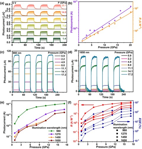
Enhancing the response of optoelectronic materials is still an immense challenge for developing the functionalities and applications of high-performance NIR photodetectors. Hence, we used several specific NIR wavelength lasers as the light source, including 980, 1270, 1450, and 1650 nm, as shown in Figure (c,d) and Figure S3a and b, to observe the variation in the photoelectric properties of WS2 under applied pressures up to 17.2 GPa. Similar to the variation observed under xenon lamp illumination, when compared with the photocurrents of WS2 under ambient pressure (Figure S4), the photocurrent increased significantly upon the application of pressure under illumination of different NIR wavelengths. It is worth mentioning that, as shown in Figure (e), in the spectral range of 1450–1650 nm, the pressure-induced photocurrent increasement reaches up to three orders of magnitude compared with the initial pressure. The external quantum efficiency (EQE) is another important parameter for photoelectric behavior characterization and can be calculated using the relationship
(2)
(2) where c is the light velocity, e is the electron charge, and λ is the wavelength of illumination. As shown in Figure (f), under the illumination of the selected NIR wavelengths, the photoelectric characteristic parameters R and EQE, like the photocurrent, exhibit a significant increase upon compression. As the pressure increases to 17.2 GPa, WS2 exhibits an increase of approximately two orders of magnitude in R and EQE in the NIR region relative to the initial pressure. Intriguingly, although the pressure leads to an enhancement of the photoelectric properties throughout the NIR waveband, the photoelectric properties at shorter wavelengths is consistently better than those at longer wavelengths, as shown in Figure (e,f). This is in good agreement with the optical absorption properties of WS2 obtained from our theoretical calculation results (the insets in Figure (b,d)). Furthermore, we compared the photocurrent at 0.5 GPa in the compression process with that under ambient pressure after decompression. We surprisingly found that the photocurrent of WS2 after compression treatment is seven times as large as that at 0.5 GPa (upon compression), as shown in Figure S3c. This indicates that pressure is of great significance as a means of adjusting high-performance infrared photodetectors.
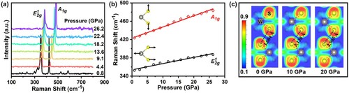
To further understand the mechanism of the pressure-modified photoelectric property enhancement of WS2, in-situ XRD and Raman spectroscopy measurements were conducted to decipher the structural modification upon compression. It can be seen in Figure S5 that when the applied pressure is up to 21.8 GPa, the in-situ high-pressure XRD patterns prove that there is no structural phase transition occurring within pressures up to 21.8 GPa, suggesting that the pressure-influenced enhancement of photoelectronic properties is not associated with it. To provide insight into the effects of the applied pressure, we investigated the Raman spectra of WS2. As shown in Figure (a), at 0.8 GPa, due to the 514.5 nm excitation wavelength is close to the B excitonic resonance for WS2, there are several second-order Raman peaks could be observed in the Raman spectrum. As the pressure increases, the B exciton energy shows a blue shift, and the second-order Raman vibration modes disappeared above 4.4 GPa (as shown in Figure S6), which is consistent with the previous literature results [Citation63]. Besides that, there are two obvious first-order Raman peaks at ∼355 and 421 cm−1 that belong to (in-plane vibrational mode of W and S atoms) and A1g (out-of-plane S-atom vibrational mode) during the whole compression process. With an increase in pressure, these two Raman modes undergo rapid hardening (Figure (b)). The slope of the A1g vibration mode is larger than that of the
mode, which is not only indicating the A1g mode is more responsive to the external pressure, but also means the S-S interlayer interaction is enhanced under compression. To further understand the chemical bonding, we performed calculations on the electron localization function (ELF), as shown in Figure (c). The enhanced interlayer interaction is also evident from the evolution of the S-S interlayer distances that reduce from 3.604 Å at ambient pressure to 2.965 Å at 20 GPa. The Raman spectra and ELF calculations reveal that the reduction of the interlayer spacing leads to the enhancement of S-S interlayer interaction upon compression.
Figure 4. (a) Raman spectra of WS2 with 514.5 nm laser excitation wavelength at selected pressures. (b) Raman shifts of the and A1g Raman modes with increasing pressure. (c) ELF of WS2 at selected pressures.
To explicitly provide information regarding the orbitals involved in the charge transfer of the band structure, we also performed theoretical calculations of the WS2 electronic structure under different pressures using the VASP as shown in Figure S7. Upon compression, the bandgap of WS2 shows a successive decrease due to the broadening of valence band maxima and conduction band minima with the contribution of the W 5d and Se 3p orbitals. Similar to MoS2 and ReS2, the enhanced S-S interlayer interaction of WS2 leads to a reduction in the bandgap during compression [Citation42,Citation47,Citation64]. The narrowed bandgap causes the valence electrons to be more easily excitable by illumination, such that they may cross over the bandgap into the conduction band, resulting in more photo-generated carriers, eventually causing higher photocurrents during compression [Citation42,Citation65].
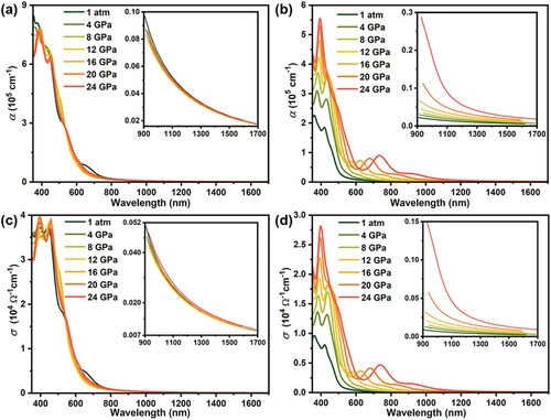
Evaluating the variations of optical parameters (particularly the absorption coefficient α(ω) and the photoconductivity σ(ω) obtained by theoretical calculations) with pressure facilitates the further understanding of the photoelectric properties of WS2 under high pressure. As shown in Figure , under ambient pressure, the α(ω) and σ(ω) is consistent with the experimental results [Citation66,Citation67], which proves the reliability of the theoretical calculations. With the increase of pressure, α(ω) and σ(ω) both increase to varying degrees, which is in accordance with our experimental observation of pressure-induced photocurrent increases. In addition, as shown in Figure S2a, the slope change of I–V curves for WS2 under xenon lamp irradiation also provides reliable evidence of the increasing trend of σ(ω) with increasing pressure. However, the α(ω) and σ(ω) are anisotropic, with considerably different values for different incident light polarization directions. Upon compression, the α(ω) and σ(ω) perpendicular to c axis are almost unchanged (Figure (a,c)); however, these two parameters parallel to c axis exhibit a significant enhancement and redshift. These results suggest the experimentally enhanced photoelectric properties of WS2 during compression is principally attributable to changes in the optical parameters along the c axis, and the red-shifted absorption edge is attributable to the pressure-induced bandgap reduction.
Figure 5. Optical properties of WS2 at various pressures. (a) Absorption coefficient α(ω) and (c) the photoconductivity σ(ω) of WS2 perpendicular to c axis at selected pressures. The (b) α(ω) and (d) σ(ω) parallel to c axis under pressure, respectively. The four inset images illustrate the changes in the WS2 optical properties in the NIR waveband.
Conclusion
In summary, we investigated the photoelectric properties and structural changes of WS2 under pressure through in-situ XRD, Raman spectroscopy, photocurrent measurements, and theoretical calculations. The WS2-based photodetector prepared in the pressure cell exhibits an ultra-fast response speed of ∼35 μs and a broad photodetection range up to 1650 nm. Moreover, the photoelectronic properties of WS2 are significantly enhanced from the visible to the NIR range upon the application of pressure. Extensive high-pressure spectroscopic analyses and theoretical calculations reveal that upon compression, more photogenerated carriers are modulated by the decrease in the WS2 bandgap owing to the enhanced S-S interlayer interaction, leading to significantly enhanced photoelectric characteristics of WS2. The employment of high pressure as a modulation strategy leads to a remarkable enhancement in the photoelectronic properties of WS2. Our work provides an experimental and theoretical basis for the practical application of WS2 as a functional material in future optoelectronic devices.
Supplemental Material
Download MS Word (3.4 MB)Disclosure statement
No potential conflict of interest was reported by the author(s).
Additional information
Funding
References
- Kim S, Lim YT, Soltesz EG, et al. Near-infrared fluorescent type II quantum dots for sentinel lymph node mapping. Nat Biotechnol. 2004;22(1):93–97.
- Rogalski A, Antoszewski J, Faraone L. Third-generation infrared photodetector arrays. J Appl Phys. 2009;105(9):091101.
- Lin CH, Liu CW. Metal-insulator-semiconductor photodetectors. Sensors. 2010;10(10):8797–8826.
- Tong XW, Zhang ZX, Wang D, et al. Inorganic CsBi3I10 perovskite/silicon heterojunctions for sensitive, self-driven and air-stable NIR photodetectors. J Mater Chem C. 2019;7(4):863–870.
- Jacoutot P, Scaccabarozzi AD, Zhang TY, et al. Infrared organic photodetectors employing ultralow bandgap polymer and non-hullerene acceptors for biometric monitoring. Small. 2022;18(15):2200580.
- Geim AK, Novoselov KS. The rise of graphene. Nat Mater. 2007;6(3):183–191.
- Neto AH C, Guinea F, Peres NMR, et al. The electronic properties of graphene. Rev Mod Phys. 2009;81(1):109–162.
- Island JO, Steele GA, van der Zant HSJ, et al. Environmental instability of few-layer black phosphorus. 2D Mater. 2015;2(1):011002.
- Singh AK, Kumbhakar P, Krishnamoorthy A, et al. Review of strategies toward the development of alloy two-dimensional (2D) transition metal dichalcogenides. Iscience. 2021;24(12):103532.
- Kumbhakar P, Chowde Gowda C, Tiwary CS. Advance optical properties and emerging applications of 2D materials. Front Mater. 2021;8:721514.
- Murali A, Lokhande G, Deo KA, et al. Emerging 2D nanomaterials for biomedical applications. Mater Today. 2021;50:276–302.
- Zheng L, Wang XW, Jiang HJ, et al. Recent progress of flexible electronics by 2D transition metal dichalcogenides. Nano Res. 2022;15(3):2413–2432.
- Bernardi M, Palummo M, Grossman JC. Extraordinary sunlight absorption and one nanometer thick photovoltaics using two-dimensional monolayer materials. Nano Lett. 2013;13(8):3664–3670.
- Chhowalla M, Shin HS, Eda G, et al. The chemistry of two-dimensional layered transition metal dichalcogenide nanosheets. Nat Chem. 2013;5(4):263–275.
- Chimene D, Alge DL, Gaharwar AK. Two-dimensional nanomaterials for biomedical applications: emerging trends and future prospects. Adv Mater. 2015;27(45):7261–7284.
- Choi W, Choudhary N, Han GH, et al. Recent development of two-dimensional transition metal dichalcogenides and their applications. Mater Today. 2017;20(3):116–130.
- Lu QP, Yu YF, Ma QL, et al. 2D transition-metal-dichalcogenide-nanosheet-based composites for photocatalytic and electrocatalytic hydrogen evolution reactions. Adv Mater. 2016;28(10):1917–1933.
- Siddique S, Gowda CC, Demiss S, et al. Emerging two-dimensional tellurides. Mater Today. 2021;51:402–426.
- Xie C, Zeng L, Zhang Z, et al. High-performance broadband heterojunction photodetectors based on multilayered PtSe2 directly grown on a Si substrate. Nanoscale. 2018;10(32):15285–15293.
- Kumbhakar P, Gowda CC, Mahapatra PL, et al. Emerging 2D metal oxides and their applications. Mater Today. 2021;45:142–168.
- Coleman JN, Lotya M, O'Neill A, et al. Two-dimensional nanosheets produced by liquid exfoliation of layered materials. Science. 2011;331(6017):568–571.
- Eda G, Yamaguchi H, Voiry D, et al. Photoluminescence from chemically exfoliated MoS2. Nano Lett. 2011;11(12):5111–5116.
- Li H, Lu G, Wang Y, et al. Mechanical exfoliation and characterization of single- and few-layer nanosheets of WSe2, TaS2, and TaSe2. Small. 2013;9(11):1974–1981.
- Xie C, Mak C, Tao X, et al. Photodetectors based on two-dimensional layered materials beyond graphene. Adv Funct Mater. 2017;27(19):1603886.
- Zhao WJ, Ghorannevis Z, Chu LQ, et al. Evolution of electronic structure in atomically thin sheets of WS2 and WSe2. Acs Nano. 2013;7(1):791–797.
- Cong CX, Shang JZ, Wu X, et al. Synthesis and optical properties of large-area single-crystalline 2D semiconductor WS2 monolayer from chemical vapor deposition. Adv Opt Mater. 2014;2(2):131–136.
- Gusakova J, Wang XL, Shiau LL, et al. Electronic properties of bulk and monolayer TMDs: theoretical study within DFT framework (GVJ-2e method). Phys Status Solidi A. 2017;214(12):1700218.
- Perea-Lopez N, Elias AL, Berkdemir A, et al. Photosensor device based on few-layered WS2 films. Adv Funct Mater. 2013;23(44):5511–5517.
- Zeng LH, Tao LL, Tang CY, et al. High-responsivity UV-Vis photodetector based on transferable WS2 film deposited by magnetron sputtering. Sci Rep. 2016;6:20343.
- Lan CY, Zhou ZY, Zhou ZF, et al. Wafer-scale synthesis of monolayer WS2 for high-performance flexible photodetectors by enhanced chemical vapor deposition. Nano Res. 2018;11(6):3371–3384.
- Li JY, Han JF, Li HX, et al. Large-area, flexible broadband photodetector based on WS2 nanosheets films. Mat Sci Semicon Proc. 2020;107:104804.
- Yao JD, Zheng ZQ, Shao JM, et al. Stable, highly-responsive and broadband photodetection based on large-area multilayered WS2 films grown by pulsed-laser deposition. Nanoscale. 2015;7(36):14974–14981.
- Abid PS, Islam SS. Broadband photodetection in wide temperature range: layer-by-layer exfoliation monitoring of WS2 bulk using microscopy and spectroscopy. J Appl Phys. 2019;125(15):154303.
- Wang HT, Yuan HT, Hong SS, et al. Physical and chemical tuning of two-dimensional transition metal dichalcogenides. Chem Soc Rev. 2015;44(9):2664–2680.
- Yang LM, Majumdar K, Liu H, et al. Chloride molecular doping technique on 2D materials: WS2 and MoS2. Nano Lett. 2014;14(11):6275–6280.
- Ou TJ, Liu CL, Yan HC, et al. Effects of pressure on the ionic transport and photoelectrical properties of CsPbBr3. Appl Phys Lett. 2019;114(6):062105.
- Guo SH, Bu KJ, Li JW, et al. Enhanced photocurrent of all-inorganic two-dimensional perovskite Cs2PbI2Cl2 via pressure-regulated excitonic features. J Am Chem Soc. 2021;143(6):2545–2551.
- Bu KJ, Luo H, Guo SH, et al. Pressure-regulated dynamic stereochemical role of lone-pair electrons in layered Bi2O2S. J Phys Chem Lett. 2020;11(22):9702–9707.
- Wen T, Zhang Q, Li NN, et al. Structural phase transition, optical and electrical property evolutions of thiospinel AgIn5S8 under high pressure. lnorg Chem. 2019;58(19):12628–12634.
- Li ZL, Li HY, Liu NN, et al. Pressure engineering for extending spectral response range and enhancing photoelectric properties of iodine. Adv Opt Mater. 2021;9(21):2101163.
- Yuan YF, Zhang ZT, Wang WK, et al. Pressure-induced enhancement of optoelectronic properties in PtS2. Chinese Phys B. 2018;27(6):066201.
- Wang P, Wang YG, Qu JY, et al. Pressure-induced structural and electronic transitions, metallization, and enhanced visible-light responsiveness in layered rhenium disulphide. Phys Rev B. 2018;97(23):235202.
- Tiong KK, Ho CH, Huang YS. The electrical transport properties of ReS2 and ReSe2 layered crystals. Solid State Commun. 1999;111(11):635–640.
- Zhao YD, Qiao JS, Yu P, et al. Extraordinarily strong interlayer interaction in 2D layered PtS2. Adv Mater. 2016;28(12):2399–2407.
- Sato Y, Nishimura T, Duanfei D, et al. Intrinsic electronic transport properties and carrier densities in PtS2 and SnSe2: exploration of n(+)-source for 2D tunnel FETs. Adv Electron Mater. 2021;7(12):2100292.
- Cui Q, He J, Bellus MZ, et al. Transient absorption measurements on anisotropic monolayer ReS2. Small. 2015;11(41):5565–5571.
- Nayak AP, Yuan Z, Cao B, et al. Pressure-modulated conductivity, carrier density, and mobility of multi layered tungsten disulfide. Acs Nano. 2015;9(9):9117–9123.
- Jäger-Waldau A, Lux-Steiner MC, Jäger-Waldau G, et al. WS2 thin films prepared by sulphurization. Appl Surf Sci. 1993;70:731–736.
- Shang JM, Chen P, Zhang LM, et al. The electronic and optical properties of tungsten disulfide under high pressure. Chem Phys Lett. 2016;651:257–260.
- Esfandiari M, Kamaei S, Rajabali M, et al. Formation of few- and monolayered WS2 sheets using plasma-treated dimethyl-sulfoxide solvent-based exfoliation. Phys Status Solidi. 2020;14(2):1900396.
- Ahmad H, Rashid H. 405 nm ultraviolet photodetector based on tungsten disulphide thin film grown by drop casting method. J Mod Opt. 2019;66(18):1836–1840.
- Chen Y. Growth of a large, single-crystalline WS2 monolayer for high-performance photodetectors by chemical vapor deposition. Micromachines. 2021;12(2):137.
- Lan CY, Kang XL, Wei RJ, et al. Utilizing a NaOH promoter to achieve large single-domain monolayer WS2 films via modified chemical vapor deposition. Acs Appl Mater Inter. 2019;11(38):35238–35246.
- Lan CY, Li C, Yin Y, et al. Large-area synthesis of monolayer WS2 and its ambient-sensitive photo-detecting performance. Nanoscale. 2015;7(14):5974–5980.
- Huo NY, Yang SX, Wei ZM, et al. Photoresponsive and gas sensing field-effect transistors based on multilayer WS2 nanoflakes. Sci Rep. 2014;4:5209.
- Xie C, Lu XT, Ma MR, et al. Catalyst-free vapor-solid deposition growth of beta-Ga2O3 nanowires for DUV photodetector and image sensor application. Adv Optical Mater. 2019;7(24):1901257.
- Guo N, Hu WD, Liao L, et al. Anomalous and highly efficient InAs nanowire phototransistors based on majority carrier transport at room temperature. Adv Mater. 2014;26(48):8203–8209.
- Lan CY, Li C, Wang S, et al. Highly responsive and broadband photodetectors based on WS2-graphene van der Waals epitaxial heterostructures. J Mater Chem C. 2017;5(6):1494–1500.
- Binet F, Duboz J, Rosencher E, et al. Mechanisms of recombination in GaN photodetectors. Appl Phys Lett. 1996;69(9):1202–1204.
- Tong XW, Kong WY, Wang YY, et al. High-performance red-light photodetector based on lead-free bismuth halide perovskite film. Acs Appl Mater Interfaces. 2017;9(22):18977–18985.
- Xie C, Wang Y, Zhang ZX, et al. Graphene/semiconductor hybrid heterostructures for optoelectronic device applications. Nano Today. 2018;19:41–83.
- Yang YT, Fang WH, Benderskii A, et al. Strain controls charge carrier lifetimes in monolayer WSe2: ab initio time domain analysis. J Phys Chem Lett. 2019;10(24):7732–7739.
- Thomas A, Vikram K, Muthu DVS, et al. Structural phase transition from 1H to 1 T ‘ at low pressure in supported monolayer WS2: Raman study. Solid State Commun. 2021;336:114412.
- Nayak AP, Bhattacharyya S, Zhu J, et al. Pressure-induced semiconducting to metallic transition in multilayered molybdenum disulphide. Nat Commun. 2014;5:3731.
- Li ZL, Li QJ, Li H, et al. Pressure-tailored band engineering for significant enhancements in the photoelectric performance of CsI3 in the optical communication waveband. Adv Funct Mater. 2022;32(8):2108636.
- Tonti D, Varsano F, Decker F, et al. Preparation and photoelectrochemistry of semiconducting WS2 thin films. J Phys Chem B. 1997;101(14):2485–2490.
- Ballif C, Regula M, Levy F. Optical and electrical properties of semiconducting WS2 thin films: from macroscopic to local probe measurements. Sol Energy Mater Sol Cells. 1999;57(2):189–207.