
 ?Mathematical formulae have been encoded as MathML and are displayed in this HTML version using MathJax in order to improve their display. Uncheck the box to turn MathJax off. This feature requires Javascript. Click on a formula to zoom.
Abstract
We report the fabrication of p-n+ diamond homojunction through an innovative approach of laser irradiation in liquid-ambient. A shallow phosphorus-doped layer with a high electric conductivity is processed on top of a p-type diamond substrate to form the p-n+ homojunction. The current–voltage measurements at room temperature confirmed high conductivity of the induced n+ layer and showed exceptional rectification properties with an ideality factor of 1.07, excellent low on-resistance of 3.7 × 10⁻² Ωcm2, and current density over 260 Acm−2 at forward-biasing of 10 V. Furthermore, undetectable leakage-current provides a rectification ratio exceeding 1010 at ±6 V, promoting the junction in UV detection applications.
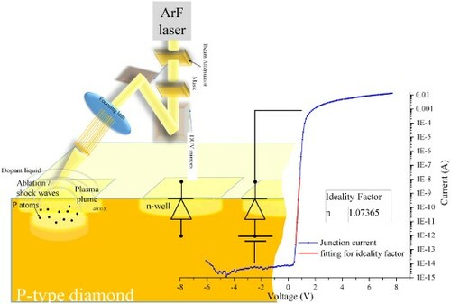
GRAPHICAL ABSTRACT
IMPACT STATEMENT
The process allows further selective and feasible patterned/shallow doping of diamond surfaces beyond the conventional methods, with minimal power consumption and fast production rate, providing more readily electrically contacted devices.
Introduction
Homoepitaxial diamond attracts considerable attention, targeting exceptional diamond properties of wide bandgap and high breakdown voltage [Citation1,Citation2]. Especially with diamond extreme radiation hardness, it is the prime element for processing detection devices such as beam-monitoring, particle-tracking, or UV detectors [Citation3,Citation4]. In addition, its high charge carrier mobilities implement faster responses in electronic switches [Citation5,Citation6]. As compared to conventional semiconductor materials, diamond-based devices yield exceptionally low leakage current, affluent responsivity, and operate in harsh environments, promoting the device industry [Citation7,Citation8]. However, with such superior diamond characteristics, it is challenging to obtain n-type conduction due to the deep donor state, and candidate donors with shallow energy levels are challenging to incorporate [Citation9]. In addition, metal-diamond interfaces greatly complicate the fabrication of the diamond devices [Citation10–12]. Practical diamond p-n junction requires a low-resistivity heavily-doped layer to avoid voltage loss and Joule heating [Citation13]. Recent studies have reported hetero-epitaxial junctions between diamond and other n-type low-resistivity semiconductors. Yet, there are few studies regarding homo-epitaxial diamond p–n junctions with high conductivity doped layers [Citation14].
Recently, laser processing of wide bandgap materials has been extensively investigated due to its high spatial resolution, temporal coherence, and ability to deliver laser pulses with enormous intensity [Citation15–18]. Thus, laser processing is considered the prime candidate for shallow junction and smaller devices processing [Citation19]. Previously, we confirmed efficient dopants incorporation to the sub-surface layers of the monocrystalline diamond through nanosecond pulsed laser irradiation [Citation20–22]. Due to ultrafast quenching from laser-induced molten phase, heavy doping exceeding equilibrium thermodynamic solubility limits could be achieved while activating carriers in a single process with no need for subsequent annealing. Dissimilar to ion implantation, which tends to form structural defects, complex amorphous/graphite phases, and generate vacancies that compensate the implanted dopants [Citation23,Citation24]. In the presented study, we demonstrate the fabrication of a homoepitaxial diamond p–n+ junction by processing a heavily phosphorus-doped layer through liquid-immersion excimer laser irradiation on a lightly boron-doped p-type substrate grown by Chemical Vapor Deposition (CVD). We investigated junction formation by laser irradiation, and its application in UV detection, as a novel technique for devices fabrication.
Experimental methods
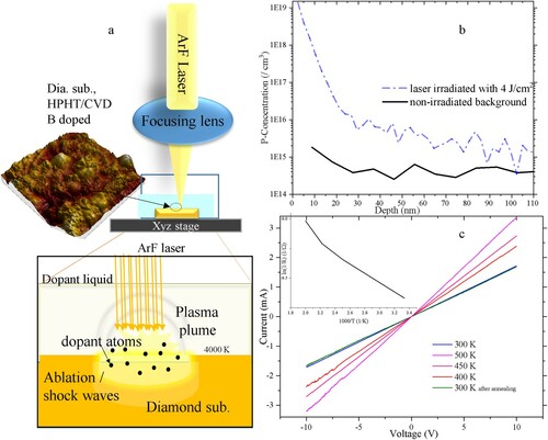
Monocrystalline p-type diamond substrates were immersed in 85% phosphoric acid (H3PO4) and irradiated with pulsed Argon Fluoride (ArF) nanosecond laser (193 nm, pulse width 20 ns). A laser beam with different profile dimensions is focused on the immersed substrates and irradiated at room temperature/pressure conditions, as shown in Figure (a). Following laser irradiations, the electrical characteristics of irradiated areas were deduced from current–voltage (I-V) measurements using a computer-controlled (Keithley 2612) source meter and low-current electrometer (Keysight B2985A). Prior to electrical measurements, the irradiated diamond substrates were cleaned by a boiling acids admixture of H2SO4:HNO3 [3:1] at 250°C. The direct placing of tungsten probes could evaluate the electric properties of irradiated areas as it could easily initiate the required ohmic properties with irradiated surfaces. Therefore, the conventional metallic ohmic electrodes are not required. The Phosphorus atoms incorporation was measured by Secondary Ion Mass Spectrometry (SIMS) in a standard facility available at the Foundation for Promotion of Material Science and Technology (MST-JP) (8.0 kV-accelerated primary ions of Cs+, and ϕ 30 μm probe-area). For SIMS experimental investigation, insulating Ib HPHT substrates were employed to confirm dopants incorporation. Furthermore, Atomic Force Microscopic measurements (Nano RTM, close contact mode) are conducted for estimating average surface roughness. The stability of electrical properties and quality of laser-irradiated areas were examined under the harsh irradiation with white-beam X-ray (10 MGy irradiation dose, 2.5 MGy/hr, beam area (400 × 14) mm2) available at SAGA Synchrotron Light Source (Saga-Ls-BL09).
Figure 1. (a) Schematic diagram of irradiation process (b) Phosphorus concentration depth profile into the diamond substrate. (c) I-V at different temperatures showing RT current returns to almost the same value before annealing. Inset shows the temperature dependence of electrical resistivity.
Results and discussion
Initially, the laser-induced doping processes were conducted on HPHT insulating diamond substrates (Sumi. Elec.) to confirm dopants incorporation and electrical conductivity enhancement is activated by phosphorus incorporation. The laser process formed irradiated areas having nearly identical shape and size as the predesignated laser beam profile. It further showed some non-homogeneity of color inside same irradiated spot, that can be attributed to the different densities in the same pulse profile due to deflection interference at the laser apparatus limiting slits and laser long path from source to sample that could be affected with ambient conditions [Citation25,Citation26]. Thus, in addition to the ablation process itself, diamond surface roughness increased from 2 to 11 nm as estimated from AFM measurements Figure (a). In Figure (b), the depth profile of irradiated HPHT diamond substrate, obtained from SIMS measurements, shows the incorporation of phosphorus dopant atoms within a depth of 50 nm upon laser irradiation with 50 shots at 4 J/cm2 and 1s repetition rate. Temperature modeling of the irradiation process further confirmed that it is mainly affecting the surface sub-layers with penetration depth of only few tens of nanometers with high spatial resolution and minimum stress on the surrounding diamond. The peak temperatures drastically increase with increasing fluences, manipulating irradiation parameters, including laser intensity and frequency, would significantly enhance the dopant incorporation profile and increase the electrical conductivity [Citation21]. Further details are provided in the supplemental material regarding process modeling and diagnostic of substrate reflectivity.
I-V measurements were conducted by directly placing tungsten probes with the irradiated HPHT surfaces. An acid mixture is applied for substrate cleaning whenever electrical characterization is performed. Thus, cleaning the surface from any metallic or possible graphite-like residuals. Adsorbate oxygen during the acid treatment is stable at moderate temperatures, and suppresses surface conduction by reducing dangling bonds density through O-termination [Citation27]. This confirms that any obtained conductivity would be mainly induced by dopant species considering the original HPHT substrates high resistivity 1012 ∼1014 Ω cm, initiating a high potential barrier with typically employed metal contacts. Owing to the high dopant concentration induced by laser irradiation, laser processed areas revealed high conductivities with low activation energies enough to demonstrate ohmic properties by directly contacting probe-heads without introducing any metal electrodes deposition. The absence of Schottky behaviors between the probe’s head and irradiated areas confirms that laser-induced dopants incorporation reduced specific contact resistivities significantly. Accordingly, it exhibited a clear linear response, as shown in Figure (c), with no hysteresis in electrical conduction before and after the heating process. Resistivity was roughly estimated to be 5 × 10⁻² Ω.cm, three orders lower compared to previously reported studies [Citation28]. The resistivity was measured by the four-probe method and calculated based on the following equation [Citation29]:
(1)
(1) where l, w, and t are dimensions of the irradiated areas, s is the electrode spacing, I and V are the applied current and measured voltage respectively. Due to small thickness of the irradiated area and its finite shape, T and F are correction factors to compensate for small thickness compared to probe spacing, and the limiting contour due to finite dimensions of the irradiated area. Semiconducting properties of irradiated areas could be realized as shown in the inset of Figure (c), with activation energies between 0.12 to 0.2 eV depending on the irradiation parameters, which is comparable to results obtained for heavily doped diamond [Citation30–32]. The variation of its slope proposes a potential modulation in carrier transport mechanism [Citation33,Citation34]. The increased conduction at room temperature (RT) also indicates that hopping conduction predominates, and band conduction is more likely to dominate at higher temperatures. Furthermore, the irradiated area was not affected with radiation exposure and maintained its electrical properties after extreme radiation with 10 MGy of white-beam X-ray. This promotes the laser processing of diamond for shallow doping and fabrication of devices employed in harsh radiation applications.
For the formation of p-n+ homojunction, the insulating diamond substrates used in the previous experiment were replaced by boron doped p-type substrates, followed by laser irradiation processes.
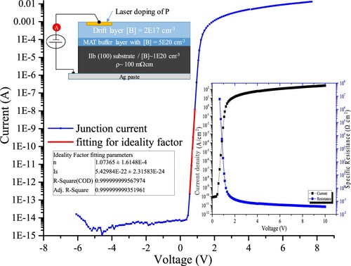
The base is an HPHT-grown p+(100) substrates 3 × 3 mm2 (TISNCM, Russia) with boron concentration of 1020 cm−3 and resistivity of 100 mΩ.cm to facilitate ohmic contacting. Lightly doped p− drift layer was homo-epitaxially grown by microwave plasma-enhanced (MW) CVD with a total gas flow of 500 sccm and CH4/H2 ratio of 4.2%. The substrate temperature and internal pressures were 1100°C and 120 Torr, respectively. Metal-assisted termination (MAT) is employed to annihilate threading dislocations through in-situ incorporation of metal impurities [Citation35,Citation36]. Therefore, a MAT buffer layer heavily doped with Tungsten was homo-epitaxially grown by Hot Filament CVD prior to the drift layer for suppression of leakage current. The sample is then immersed in phosphoric acid H3PO4 and irradiated with ArF laser to process phosphorus-doped regions acting as n-type wells.
Figure shows the schematic diagram of the demonstrated structure and typical room-temperature I–V characteristics of the p–n+ junction. The I-V results disclosed optimal diode properties with undetectably low leakage current at reverse biased conditions. The fabricated junction revealed an excellent rectification ratio of 1011 at ±6 V, ideality factor of n = 1.07, and saturated current Io = 5.4E-22 A. At forward bias, the junction demonstrated an adequately low specific on-resistance of 3.7 × 10⁻² Ω.cm2, providing a high current density exceeding 250 A/cm2 just at 10 V. The outstanding junction characteristics are mainly assigned to the high conductivity of the laser-induced phosphorus-doped layer and high quality of the fabricated homojunction with less induced defects. In addition, the inclusion of the MAT layer resulted in a significant reduction of threading dislocations and greatly suppressed dislocations or dislocation bundles from affecting the p-n+ junction interface. Further discussion on the crystalline quality and Raman measurements of laser-irradiated areas are included in the supplemental data.
Figure 2. Current-voltage properties of a vertical type p–n+ homo-junction measured at room temperature. Inset shows J-V and the specific on-resistance properties under forward biased condition.
The dopant incorporation and conductivity levels could be controlled by manipulating laser irradiation parameters. Figure (a) shows different n-type wells (P-doped) processed at different conditions to yield different doping levels. The p− drift layer with a uniform thickness of 3 μm was homoepitaxially grown by MWCVD on EDP (100) substrate after the insertion of the MAT buffer layer with 2 μm thickness. Heavily boron doped wells B1 and B2 were processed through laser irradiation with liquid immersion in H3BO3 on the substrate surface acting as ohmic contacts. Areas P1, P2, and P3 were processed through H3PO4 acid-emersion excimer-laser irradiation with conditions starting from high (500 shots-5.3 J/cm2 for P1) and decreased down to (100 shots-4.8 J/cm2 for P3). Such alteration of irradiation conditions resulted in differences in the obtained conductivity for each area as shown in Figure (a). Areas irradiated at higher laser-fluence, and larger number of shots (P1) exhibited higher conductivity compared to other areas (P2 and P3) owing to the induced heavier dopants incorporation. Accordingly, the possibility of tunneling through the junction increases and the junction leakage current increases with heavy doping of the n side as shown in Figure (b).
Figure 3. (a) Electrical characteristics of P-doped irradiated areas, altering irradiation parameters modifies dopant-incorporation and electrical-conductivity. (b) Dark I-V measurements for lateral p-n+ junctions showing leakage current increasing with heavy doping of the n side. (c) I−V property of the B1-P3 p–n+ junction at different temperatures. Inset shows ideality factor variation with temperature.
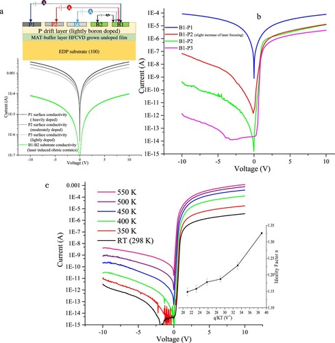
Temperature dependence of current–voltage characteristics demonstrated a slight increase in the leakage current with temperature, while the rectification ratio is kept intact over five orders of magnitude at a high temperature of 525 K as shown in Figure (c). Inset shows that diode parameters such as the ideality factor n is found to be dependent on the diode temperature. The value of Richardson constant (A*) deduced from temperature dependence of saturation-current was much lower than the theoretical value (90 A/cm2.K2). Such deviations from ideality suggest insufficiency of the conventional TE model to thoroughly demonstrate the pn junction behavior [Citation37–40]. Especially with dependence of saturation current on the diffusion length and diffusion constant of the injected minority carriers, rather than thermionic emission of the semiconductor's majority carriers as in schottky diodes [Citation41]. In addition, in lateral type pn junctions, it is hard to determine saturation current contribution owing to three-dimensional diffusion of minority carriers in the bulk. Thus, for better estimation of the bandgap, capacitance measurements were conducted.
Figure (a) shows capacitance variation with frequency at different applied voltages and different temperatures. Inconsistent with ideal p-n junction behavior, the measured capacitance decreased at high frequencies, which refers to a space charge layer within the junction. This observation is attributed to the deep acceptors in the p-type side that are incapable of following the high-frequency voltage modulation. Commonly, the space charge region consists of both transition as well as depletion layers. Both donor and acceptor atoms are partially ionized at room temperature in the transition region. When the temperature increases, the transition layer length decreases, which is also associated with the net density of dopants [Citation14,Citation42]. Due to the laser-induced area's high conductivity and heavy dopant concertation compared to the p-type substrate, the depletion region would expand mainly on the p-type side. Thus, the frequency range increases with increasing temperature because of the diamond resistivity and the dispersion effect of deep-level acceptors. The capacitance increases as well with temperature, depending on applied voltage values since it further affects the depletion layer width.
Figure 4. (a) Capacitance variation with frequency, at different voltages and temperatures. (b) C-V characteristics of the lateral junction and deduced built-in potential from the reciprocal slope of C−2-V.
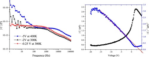
For diamond homojunction, to estimate the built-in potential, it is preferred to neglect the effect of deep dopants and transition layer [Citation43]. Thus, C–V measurements are commonly conducted at adequately low frequencies or high temperatures. However, such phenomena is ignored for semiconductor devices, as the capacitance values are generally derived from a series-mode measurement of LCR meter and measured independent of any series resistance. Figure (b) shows C–V measurements conducted at an intermediate frequency within the frequency bandwidth spectrum at 400 K. The capacitance exhibited a gradual increase with increasing the bias voltage, which confirms the presence of a space-charge region increasing in width with decreasing the bias voltage. The estimated built-in potential was 3.9 V from the reciprocal slope of the C−2–V under reverse bias conditions. C-V properties exhibited a shoulder in the forward biasing region, which could be attributed to presence of electrically active deep levels excluding that of boron or phosphorus near the junction. It is mainly observed in leaky junctions and showed a frequency dependency. Fitting of the linear region of C−2–V for multiple junctions on the same substrate reflected the gradient of doping concentration to be approximately 2 × 10¹⁵ ∼ 1.1 × 1016 cm−3 calculated according to the following equation [Citation44].
(2)
(2) This is in a great agreement with the doping concentration of the p-type substrate measured by SIMS 1 × 1016 cm−3, showing that the depletion region mostly expands to the p-type side owing to the heavy doping of the n region that exhibited conductivity 2–3 orders higher (Figure (a)) compared to the substrate. Further investigation is conducted to understand the complete behavior of laser-induced junction.
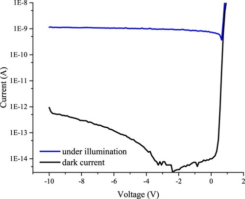
The low dark current and high stability of the pn junction promoted its application in UV detection. Up to date, most diamond-based UV detectors are mainly based on either planar metal–semiconductor-metal photoconductive detector or Schottky-barrier photodiodes [Citation45–47]. Such photodiodes face many limitations/challenges of high leakage current from defects in hetero-structures, etching processes, and multi-lithography alignments complexity [Citation48,Citation49]. Additionally, the complication of ohmic contact fabrication that usually results in space-charge build-up effects. Especially with diamond high-density and incapability to compensate for its wide bandgap [Citation50]. Therefore, reducing the average minimum ionizing particle signal generated greatly compared to other materials such as silicon, and accordingly reduces the device sensitivities [Citation51,Citation52]. Through the proposed innovative-laser processing in dopant medium, both the pn junction and ohmic contacts could be fabricated in a single process with the fastest rate of ∼ 200 s per area. Figure shows the I–V characteristics of the junction as a UV detector under 254 nm-handy UV lamp (500 μW/cm2). Since UV photons are strongly absorbed in a very thin layer [Citation53,Citation54], the previously demonstrated B1-P3 diode is employed, to utilize from its coplanar structure. A progressively smaller sub-bandgap signal (for wavelengths > 225 nm) is present, due to defect-related energy levels within the bandgap [Citation55]. The exact nature of these defects could be intrinsic as dislocations/imperfections in the diamond lattice, and extrinsic as impurities. Presence of such defects can also explain the average increase in reverse currents [Citation56]. In addition, impurities such as deep dopants, results in absorption of sub-bandgap signals, and significant increase in photocurrent upon illumination with three orders of magnitude higher than the dark current, implying a high photo to dark current ratio. The generated photocurrent started to saturate at a very low biasing voltage, indicating high device response and fast collection of photogenerated carriers, quickly reaching the space-charge-limited photocurrent. The responsivity of device is calculated using the equation R = Iph/AP [Citation57], where Iph is the net photocurrent, A is active photosensitive area(junction area of 400 × 170 μm), and P is light power density. The responsivity of the detector under 254 nm illumination at 10 V is calculated to be 3.57 mA/W. It is noteworthy here that the (500 μW/cm2) is the manufacturer power rating for the UV source, However, the actual measured power during exposure was less than 300 μW/cm2, owing to the device lifetime. Accordingly, the actual responsivity is approximately 6.1 mA/W, which is over two times larger than that of the common lens UV detector (2.32 mA/W at 220 nm) [Citation58]. Furthermore, the fabricated junction exhibited distinguished stability and reproducibility in its response, demonstrating the absence of persistent photoconductivity pumping effects, which restrain the progress of diamond-based detectors.
Figure 5. I-V characteristics of the p-n+ junction was measured at room temperature in the dark (black) and under 254 nm light illumination (blue).
Conclusion
The innovative-proposed approach of laser-induced doping and formation of p-n+ junction is intensively discussed. The laser-irradiated areas on diamond surfaces exhibited different conductivity levels varied by modifying irradiation conditions. Electrical properties of irradiated areas showed high stability, high radiation hardness, and resistance to acidic processing without inducing any hysteresis in its electrical characteristics following annealing or exposure to radiation. These findings promote the application in detection under harsh environments. The fabricated p-n+ junction revealed outstanding diode characteristics with undetectable-low leakage-current, and optimum ideality factor that is further enhanced with the inclusion of the MAT buffer layer. Furthermore, the junction exhibits high performance as a UV photodetector. Laser irradiation of diamond in liquid-ambient enabled selective, fast-patterned doping and feasible fabrication of devices those maintain diamond's high purity and durability.
Additional information
Supporting Information is provided for a detailed discussion regarding modeling of ablation temperature, and substrate optical and Raman characterization.
Supplemental Material
Download PDF (398.3 KB)Disclosure statement
No potential conflict of interest was reported by the author(s).
Correction Statement
This article has been corrected with minor changes. These changes do not impact the academic content of the article.
Additional information
Funding
References
- Kraft A. Doped diamond: a compact review on a new, versatile electrode material. Int J Electrochem Sci. 2007;2:355–385.
- Zhao S. Theoretical studies of diamond for electronic applications. 2016. http://urn.kb.se/resolve?urn=urn:nbn:se:uu:diva-283409.
- Gallin-Martel ML, Kim YH, Abbassi L, et al. Characterization of diamond and silicon carbide detectors with fission fragments. Front Phys. 2021;9:1–19.
- Liu Z, Li F, Li S, et al. Fabrication of UV photodetector on TiO 2/diamond film. Sci Rep. 2015;5:1–7. doi:https://doi.org/10.1038/srep14420.
- Amaratunga GAJ. A Dawn for carbon electronics? Science. 2002;297(80):1657–1658. doi:https://doi.org/10.1126/science.1075868.
- Kato Y, Teraji T, Power A. Key technologies for device fabrications and materials characterizations. Power Electron Device Appl Diam Semicond. 2018. doi:https://doi.org/10.1016/b978-0-08-102183-5.00004-2.
- Gole JL, Lewis SE. Porous silicon – sensors and future applications. Nanosilicon. 2008:149–175. doi:https://doi.org/10.1016/B978-008044528-1.50005-1.
- Shkir M, Khan MT, Ashraf IM, et al. High-performance visible light photodetectors based on inorganic CZT and InCZT single crystals. Sci Rep. 2019;9:1–9. doi:https://doi.org/10.1038/s41598-019-48621-3.
- Makino T, Kato H, Ri S-G, et al. Homoepitaxial diamond p-n+ junction with low specific on-resistance and ideal built-in potential. Diam Relat Mater. 2008;17:782–785. doi:https://doi.org/10.1016/j.diamond.2007.12.006.
- Nemanich RJ, Baumann PK, van der Weide J. Diamond negative electron affinity surfaces, structures and devices. United States: N. p., 1995. Web.
- Ristein J. Electronic properties of diamond surfaces – blessing or curse for devices? Diam Relat Mater. 2000;9:1129–1137. doi:https://doi.org/10.1016/S0925-9635(99)00316-7.
- Zkria A, Abubakr E, Sittimart P, et al. Analysis of electrical characteristics of Pd/n-Nanocarbon/p-Si heterojunction diodes: by C-V-f and G/w-V-f. J Nanomater. 2020;2020:1–9. doi:https://doi.org/10.1155/2020/4917946.
- Haenen K, Lazea A, Nesládek M, et al. Rectifying properties and photoresponse of CVD diamond p(i)n-junctions. Phys Status Solidi – Rapid Res Lett. 2009;3:208–210.
- Makino T, Kato H, Ogura M, et al. Electrical and optical characterizations of (001)-oriented homoepitaxial diamond p-n junction. Diam Relat Mater. 2006;15:513–516. doi:https://doi.org/10.1016/j.diamond.2005.11.021.
- Narayan J, Bhaumik A, Haque A. Pseudo-topotactic growth of diamond nanofibers. Acta Mater. 2019;178:179–185. doi:https://doi.org/10.1016/j.actamat.2019.08.008.
- Trusovas R, Račiukaitis G, Niaura G, et al. Recent advances in laser utilization in the chemical modification of graphene oxide and its applications. Adv Opt Mater. 2016;4:37–65. doi:https://doi.org/10.1002/adom.201500469.
- Zkria A, Abubakr E, Egiza M, et al. Structural evolution of laser-irradiated ultrananocrystalline diamond/amorphous carbon composite films prepared by coaxial arc plasma. Appl Phys Express. 2020;13:0–6. doi:https://doi.org/10.35848/1882-0786/abb871.
- Stock F, Antoni F, Diebold L, et al. UV laser annealing of diamond-like carbon layers obtained by pulsed laser deposition for optical and photovoltaic applications. Appl Surf Sci. 2019;464:562–566. doi:https://doi.org/10.1016/j.apsusc.2018.09.085.
- Bentini GG, Bianconi M, Summonte C. Surface doping of semiconductors by pulsed-laser irradiation in reactive atmosphere. Appl Phys A Solids Surfaces. 1988;45:317–324. doi:https://doi.org/10.1007/BF00617938.
- Abubakr E, Zkria A, Katamune Y, et al. Formation of low resistivity layers on singlecrystalline diamond by excimer laser irradiation. Diam Relat Mater. 2019;95:166–173. doi:https://doi.org/10.1016/j.diamond.2019.04.013.
- Abubakr E, Zkria A, Ohmagari S, et al. Laser-induced phosphorus-doped conductive layer formation on single-crystal diamond surfaces. ACS Appl Mater Interfaces. 2020;12:57619–57626. doi:https://doi.org/10.1021/acsami.0c18435.
- Abubakr E, Ohmagari S, Zkria A, et al. Materials science in semiconductor processing laser-induced novel ohmic contact formation for effective charge collection in diamond detectors. Mater Sci Semicond Process. 2022;139:106370. doi:https://doi.org/10.1016/j.mssp.2021.106370.
- Braunstein G, Kalish R. Effective p-type doping of diamond by boron ion implantation. J Appl Phys. 1983;54:2106–2108. doi:https://doi.org/10.1063/1.332262.
- Haque A, Sumaiya S. An overview on the formation and processing of nitrogen-vacancy photonic centers in diamond by ion implantation. J Manuf Mater Process. 2017;1:6. doi:https://doi.org/10.3390/jmmp1010006.
- Ikeda A, Nishi K, Ikenoue H, et al. Phosphorus doping of 4H-SiC by KrF excimer laser irradiation in phosphoric solution. Jpn J Appl Phys. 2013;52:06GF02. doi:https://doi.org/10.7567/JJAP.52.06GF02.
- Takahashi K, Kurosawa M, Ikenoue H, et al. Low thermal budget n-type doping into Ge(001) surface using ultraviolet laser irradiation in phosphoric acid solution. Appl Phys Lett. 2016;108:1–5. doi:https://doi.org/10.1063/1.4941236.
- Chen YG, Ogura M, Okushi H. Schottky junction properties on high quality boron-doped homoepitaxial diamond thin films. J Vac Sci Technol B Microelectron Nanom Struct. 2004;22:2084. doi:https://doi.org/10.1116/1.1768186.
- Ficek M, Sankaran KJ, Ryl J, et al. Ellipsometric investigation of nitrogen doped diamond thin films grown in microwave CH4/H2/N2 plasma enhanced chemical vapor deposition. Appl Phys Lett. 2016;108:2–7.
- Topsoe H. Geometric factors in four point resistivity measurement. Bridge Technol. 1968;472–13:58–59.
- Kato H, Takeuchi D, Tokuda N, et al. Characterization of specific contact resistance on heavily phosphorus-doped diamond films. Diamond Relat Mater. 2009;18:782–785.
- Kajihara SA, Antonelli A, Bernholc J, et al. Nitrogen and potential n-type dopants in diamond. Phys Rev Lett. 1991;66:2010–2013.
- Hu XJ, Li RB, Shen HS, et al. Electrical and structural properties of boron and phosphorus co-doped diamond films. Carbon NY. 2004;42:1501–1506.
- Sekiguchi T, Koizumi S. Characterization of a diamond p-n junction using electron-beam-induced current and cathodoluminescence. Appl Phys Lett. 2002;81:1987–1989.
- Kono S, Nohara T, Abe S, et al. Electron spectroscopic determination of electronic structures of phosphorus-doped n-type heteroepitaxial diamond (001) surface and junction. Jpn J Appl Phys. 2012;51:090109.
- Ohmagari S, Yamada H, Tsubouchi N, et al. Large reduction of threading dislocations in diamond by hot-filament chemical vapor deposition accompanying W incorporations. Appl Phys Lett [Internet]. 2018;113. Available from: doi:https://doi.org/10.1063/1.5040658.
- Ohmagari S, Yamada H, Tsubouchi N, et al. Toward high-performance diamond electronics: control and annihilation of dislocation propagation by metal-assisted termination. Phys Status Solidi Appl Mater Sci. 2019;216:1–15.
- Bhuiyan AS, Martinez A, Esteve D.. A new richardson plot for non-ideal schottky diodes. Thin Sol Film. 1988;161:93–100.
- Vescan A, Daumiller I, Gluche P, et al. Very high temperature operation of diamond Schottky diode. IEEE Electron Device Lett. Nov. 1997;18(11):556–558. doi:https://doi.org/10.1109/55.641444.
- Traoré A, Muret P, Fiori A, et al. Zr/oxidized diamond interface for high power Schottky diodes. Appl Phys Lett. 2014;104(5): Art. no. 052105. doi:https://doi.org/10.1063/1.4864060.
- Malakoutian M, Benipal M, Koeck FA, et al. Schottky barrier height Analysis of diamond SPIND using high temperature operation up to 873 K. IEEE J Electron Devices Soc. 2020;8:614–618.
- Werner JH. Schottky barrier and pn-junctionI/V plots? small signal evaluation. Appl Phys A Solids Surfaces. 1988;47:291–300.
- Koide Y. Peculiarity of depletion region in diamond pn-junction. Jpn J Appl Physics Part 1 Regul Pap Short Notes Rev Pap. 2003;42:6800–6803. doi:https://doi.org/10.1143/jjap.42.6800.
- Suzuki M, Yoshida H, Sakuma N, et al. Electrical characterization of phosphorus-doped n-type homoepitaxial diamond layers by Schottky barrier diodes. Appl Phys Lett. 2004;84:2349–2351. doi:https://doi.org/10.1063/1.1695206.
- Shimaoka T, Koizumi S, Tanaka MM. Diamond photovoltaic radiation sensor using pn junction. Appl Phys Lett [Internet]. 2018;113:1–5. Available from: doi:https://doi.org/10.1063/1.5034413.
- Liao M, Koide Y. High-performance metal-semiconductor-metal deep-ultraviolet photodetectors based on homoepitaxial diamond thin film. Appl Phys Lett. 2006;89:3–6. doi:https://doi.org/10.1063/1.2349829.
- Liao M, Koide Y, Alvarez J. Single Schottky-barrier photodiode with interdigitated-finger geometry: application to diamond. Appl Phys Lett. 2007;90:2005–2008. doi:https://doi.org/10.1063/1.2715440.
- Benmoussa A, Soltani A, Haenen K, et al. New developments on diamond photodetector for VUV solar observations. Semicond Sci Technol. 2008;23:035026. doi:https://doi.org/10.1088/0268-1242/23/3/035026.
- Chang X, Wang YF, Zhang X, et al. UV-photodetector based on NiO/diamond film. Appl Phys Lett. 2018;112:1–6. doi:https://doi.org/10.1063/1.5004269.
- Galbiati A, Lynn S, Oliver K, et al. Performance of monocrystalline diamond radiation detectors fabricated using TiW, Cr/Au and a novel ohmic DLC/Pt/Au electrical contact. IEEE Trans Nucl Sci. 2009;56:1863–1874. doi:https://doi.org/10.1109/TNS.2009.2020428.
- Makino T, Tanimoto S, Hayashi Y, et al. Diamond Schottky- pn diode with high forward current density and fast switching operation. Appl Phys Lett. 2009;94:1–4.
- Pan LS, Kania DR, editors. Diamond: electronic properties and applications; 1995. doi:https://doi.org/10.1007/978-1-4615-2257-7.
- Shimaoka T, Umezawa H, Ichikawa K, et al. Ultrahigh conversion efficiency of betavoltaic cell using diamond pn junction. Appl Phys Lett. 2020;117:103902.
- Pace E, De Sio A. Innovative diamond photo-detectors for UV astrophysics. Mem Della Soc Astron Ital Suppl. 2010;14:84.
- Whitfield MD, Chan SSM, Jackman RB. Thin film diamond photodiode for ultraviolet light detection. Appl Phys Lett 1996;68:290–292.
- Girolami M, Serpente V, Mastellone M, et al. Self-powered solar-blind ultrafast UV-C diamond detectors with asymmetric Schottky contacts. Carbon NY. 2022;189:27–36.
- Haenen K, Lazea A, Nesládek M, et al. Rectifying properties and photoresponse of CVD diamond p(i)n-junctions. Phys Status Solidi – Rapid Res Lett. 2009;3:208.
- Wu Y, Li Z, Ang K-W, et al. Monolithic integration of MoS2 -based visible detectors and GaN-based UV detectors. Photonics Res. 2019;7:1127.
- Liu Z, Zhao D, Zhu T, et al. Enhanced Responsivity of Diamond UV Detector Based on Regrown Lens Structure. IEEE Electron Device Lett 2020;41:1829–1832.