
 ?Mathematical formulae have been encoded as MathML and are displayed in this HTML version using MathJax in order to improve their display. Uncheck the box to turn MathJax off. This feature requires Javascript. Click on a formula to zoom.
Abstract
Low-dimensional materials (LDMs), due to exotic mechanical, optical and electrical properties enhanced by ultrahigh surface-to-volume ratio and quantum confinements, have taken centerstage in nanoelectromechanical system (NEMS) resonators. The ability to survive from high strains and complex environments enables LDMs-based NEMS resonators innovative effectuations for mass-, gas- and bio-sensings and computings. In this review, we highlighted the fabrication, actuation, detection, figure of merit, influence factors and recent process of LDMs-based NEMS resonators. After overviewing representative applications and feasible directions, we summarized the confronted challenges in fabrications, tunings and utilizations of LDMs-based NEMS resonators. Finally, the prospects that may properly tackle these obstacles were concluded, attempting to offer useful guidelines for both theoretical and experimental experts to promote NEMS resonators one step closer toward industrializations.
IMPACT STATEMENT
This review delineates the principles and advances of nanoelectromechanical system resonators based on low-dimensional materials, followed by promising applications, such as sensings, nano-electronics and quantum detections.
1. Introduction
Nanoelectromechanical systems (NEMS) show great potentials in the fields of sensors, biochemical monitors and radio frequency (RF) devices, owing to their high sensitivity and efficiency with low power consumption [Citation1]. Differentiating from conventional microelectromechanical systems (MEMS), NEMS integrate the electrical functionalities with mechanical ones at nanometer and even atomic level. Profiting from the reduced dimension, emerging quantum effects and interface effects in NEMS devices attracted ever-growing research efforts from the communities of physics, mechanics, materials science and chemistry [Citation2–6]. Initially, the majority of NEMS resonators relies on the thin films of metallic (Al, Au) [Citation7] and semiconducting (Si, GaAs) [Citation8] materials. With rapid advances in materials synthesis and fabrication technology, the last decades have witnessed the prosperity of versatile NEMS resonators. Although the NEMS resonators possess acceptable resonance frequency (fres) and quality factor (Q), brittleness (strain < 2% usually) and the ineluctable difficulty in further down-scaling-process greatly limit their integrations as single entities for next-generation smart devices, flexible devices and Internet of Things.
Recently, low dimensional materials (LDMs), including one-dimensional (1D) carbon nanotubes and two-dimensional (2D) family of atomically thin films with no dangling bond, [Citation9] have revolutionized material and architecture design for NEMS resonators because of their unique structures and abilities to function at extreme conditions [Citation10–14]. For instance, carbon nanotubes (CNTs) discovered by Lijima [Citation15] in 1991 show outstanding strength and electrical conductivity, surpassing the majority of conventional NEMS materials [Citation16–20]. In 2004, thin graphene flakes was isolated from graphite by Geim and his coworkers and take the centerstage for building assorted NEMS resonators owing to its ultrahigh strain limits and tunable properties [Citation21–26]. To be more specified, graphene has excellent electrical conductivity (mobility up to 106 cm/(V·s) [Citation23,Citation27]), out-of-plane flexibility, in-plane softness (Young’s modulus of 1 TPa [Citation28,Citation29]) and thermal conductivity (3.5 ∼ 5 kW/mK [Citation30]). Stimulated by the success of graphene, hexagonal boron nitride (h-BN) [Citation31,Citation32], transition metal dichalcogenides (TMDCs) [Citation33–37] and monochalcogenides (TMMCs) [Citation38], black phosphorus (BP) [Citation32,Citation39–43], MXenes [Citation44,Citation45] and van der Waals (vdW) heterostructure were excavated in succession toward high-performance NEMS applications. After prepared from mechanical exfoliation, chemical vapor deposition (CVD) and other synthesis methods, LDMs undergo a series of nanofabrication procedures to achieve suspended beam or film architecture for NEMS resonators [Citation46–49]. Actuated by external light, force, magnetism and electrical fields, the physical quantities of as-fabricated NEMS resonators are readout in terms of electrical/optical signals. In light of this operation principle, applications of LDMs-based NEMS resonators covering mass sensors, mechanical sensors, chemical and biological sensors, nano-electronics devices and quantum detection have been realized. Compared with the tremendous original predictions and experimental demonstrations of emerging LDMs-based NEMS resonators, the review upon this topic is relative lagging. Although few reports have summarized the progress of 2D NEMS, they mainly focus on 2D materials (2DMs)-based nanoelectromechanical sensing or fundamental physics [Citation50–52]. Therefore, an overview of LDMs-based NEMS resonators especially focusing on the progress of entire low-dimensional material system is still desirable.
In this review, we first summarized the classic fabrication routines (Figure ), working mechanisms, actuations, detections and primary key parameters of NEMS resonators in section 2. Subsequently, the advances in NEMS resonators from different LDMs and their heterostructure were minutely provided in section 3. In the meantime, the insightful influence of vital factors (sample thickness, geometry and operation environments) on tuning resonance frequency, quality factor and possible dissipation of resonators were summarized. Section 4 overviewed the representative applications of LDMs-based NEMS resonators. Finally, we highlighted the current challenges and put forward some perspectives that may be conducive to overcoming these bottlenecks and advancing the applications of LDMs in future multifunctional and intelligent NEMS resonators. This timing review attempts to offer both skilled and fresh researchers a guidance to accelerate the developments and applications of LDMs in high-performance and ambient-stable NEMS resonators.
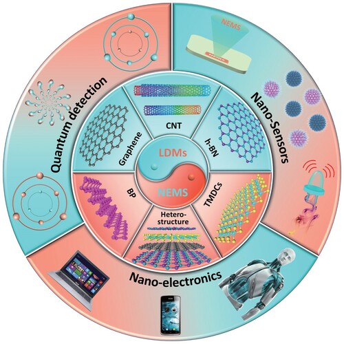
Figure 1. LDMs-based NEMS resonators in this review. The availability of diverse LDMs enabled NEMS resonators in sensings, electronics and quantum detection applications. Fundamentally, the working mechanisms, actuation and detection of representative LDMs-based NEMS resonators are included in succession.
2. NEMS resonators
Attributed to the coupling of electrical and mechanical properties at the nanometer scale, NEMS resonators maximize the operating speed and sensitivity by consuming negligible energy and thus become potential units in optical, electrical and mechanical applications [Citation25]. For NEMS resonators, the core element is the active materials. The basic premise of active materials is to survive under certain mechanical deformations and show great feasibility for device integrations. In this concern, LDMs become one promising substitute for conventional silicon in next-generation NEMS resonators. Moreover, the superiority of LDMs for NEMS resonators also lies in the tunable bandgaps, reduced dielectric screening, enhanced many-body interaction, the ability to withstand high strain and material stability in the ultra-high frequency (UHF) range. Therefore, the following section carefully reviewed the fabrication routines, mechanisms, influent factors and recent progress of LDMs-based NEMS resonators.
2.1. Fabrication methods
LDMs family for NEMS devices are usually synthesized on supporting substrates (metal foils, SiO2 and sapphire) by CVD or from mechanical exfoliations of bulk crystals. The key to fabricate operative NEMS resonators is the transfer of LDMs onto targeted substrates. According to the sequence of transfer and patterning, the fabrication process of NEMS resonators could be generally classified into two categories [Citation50] (as sketched in Figure ): (1) patterning after transfer methods, such as wet chemical etching that widely adopted for CVD samples, mechanical etching, and dry physical etching [Citation53,Citation54]. In the concern of etching methods, dry etching have relatively high selectivity but difficulty in achieving suspended structure. On the other hand, regular wet etching might achieve suspended structure but some residues or contaminations may be introduced. In the aspect of mechanical etching, it remains difficult to achieve smooth surfaces due to excessive surface impact. (2) patterning before transfer methods, where the LDMs were first exfoliated onto a transfer layer, such as polydimethylsiloxane (PDMS) stamp [Citation55–58], polymethyl methacrylate (PMMA) supporting layer and thermoplastic sacrificial layer [Citation49], and then transferred to a pre-patterned substrate by vdW pick-up [Citation47] or liquid wedging [Citation59]. For patterning before transfer methods, monolayer or multilayer 2D flakes are directly exfoliated onto targeted substrates by PMMA, PDMS and thermoplastic layer, thereby liberating active materials from water or chemical contaminations. With respect to the vdW pick-up and liquid wedging methods, desired flakes are required to be pre-exfoliated onto silicon substrates and then lift-off via vdW force or capillary force for further transfer process. Besides, vapor–liquid–solid epitaxial growth was also proved to be a feasible approach to provide LDMs for NEMS resonators and a detailed discussion will be conducted in late sections [Citation60].
Figure 2. Prevalent fabrication routines of NEMS resonators. (a) Patterning after transfer methods [Citation47]. Take wet chemical etching technique as an example. Firstly, 2D crystal was peeled onto a sacrificial membrane (1), and then covered by a resistive mask with desired patterns (2). Later, the film was etched away by chemical solution (3), followed by removing the resist mask to obtain suspended structure (4). (b) Patterning before transfer methods [Citation50]. Take an all-dry transfer technique using PDMS stamps for example. 2D crystal was first exfoliated onto a PDMS stamp and then transferred to a pre-patterned substrate with precise alignment (1). After gently pressing (2) and peeling-off the PDMS stamp with care (3), the 2D crystal was released to form suspended micro-drumheads (4). For better understanding and demonstrative purpose, suspended 2D films in well-defined regular geometry are selected here as the working materials.
![Figure 2. Prevalent fabrication routines of NEMS resonators. (a) Patterning after transfer methods [Citation47]. Take wet chemical etching technique as an example. Firstly, 2D crystal was peeled onto a sacrificial membrane (1), and then covered by a resistive mask with desired patterns (2). Later, the film was etched away by chemical solution (3), followed by removing the resist mask to obtain suspended structure (4). (b) Patterning before transfer methods [Citation50]. Take an all-dry transfer technique using PDMS stamps for example. 2D crystal was first exfoliated onto a PDMS stamp and then transferred to a pre-patterned substrate with precise alignment (1). After gently pressing (2) and peeling-off the PDMS stamp with care (3), the 2D crystal was released to form suspended micro-drumheads (4). For better understanding and demonstrative purpose, suspended 2D films in well-defined regular geometry are selected here as the working materials.](/cms/asset/f29d2622-bfba-468b-9f4a-41825d3d3f1b/tmrl_a_2111233_f0002_oc.jpg)
2.1.1 Patterning after transfer methods
Figure (a) exhibits the patterning after transfer routine for constructing LDMs-based NEMS resonators, using wet chemical etching technique as an example [Citation47,Citation53,Citation54]. Initially, LDMs were deposited or transferred onto the target substrates (polymer or SiO2), and then a mask via photolithography techniques was developed to expose the film partially. Next, supporting layers were selectively etched away by wet chemical etchants. Finally, perfect NEMS devices were completed by removing the masks [Citation47]. This method was widely employed to prepare CNTs-based NEMS devices and several 2DMs-based ones that consisting of partially covered cavities (such as rectangular 2D crystal films bridging over a 1D trench). However, several drawbacks still exist, such as the easy breaking of suspended films in solutions and subsequent drying process owing to the high surface tension of the etchants, and the residual contaminations from solutions at the film surface and edge regions, extremely reducing the quality and performances of as-fabricated NEMS resonators.
2.1.2 Patterning before transfer methods
In 2011, Castellanos-Gomez et al. [Citation56] demonstrated the transfer of few-layer graphene flakes upon mica flakes using viscoelastic stamps in an all-dry transfer manner, enabling precise manipulation of 2D flakes without the necessity of any wet chemicals and sacrificing polymer layers [Citation61–63]. Figure (b) shows the patterning before transfer process for fabricating NEMS resonators, taking as an example PDMS stamp dry transfer technology [Citation57]. 2DMs flakes were first exfoliated onto a viscoelastic PDMS stamp and then transferred onto of 2D crystals were well preserved [Citation49]. In the stamp transfer process, the applied pressure on the stamp affects the value and uniformity of the pretension distributed in the suspended membrane. As a result, the resonance frequency and stiffness of 2D membrane was affected. Moreover, non-uniform strain in the transfer layer might introduce wrinkles and nanoscale polymeric residues may be also left on 2D membrane. Despite these drawbacks, this all-dry viscoelastic stamping method show great capacity in fabricating partially suspend 2DMs on trenches with high yields [Citation50]. For instance, Xie et al. [Citation26] successfully integrated vibrating 2DMs-based NEMS onto comb-drive MEMS actuators using a similar transfer method, demonstrating feasible trans-scale integrations from nanometer to micrometer. The wide-frequency tuning of 2DMs-based NEMS resonators was realized by employing voltage-controlled comb-driving MEMS actuators to adjust the strain distribution within 2DMs. In combination with potential scaling-up productions of device arrays, patterning before transfer methods are hopeful to facilitate the commercialization of high-performance NEMS resonators.
2.1.3 Other methods
In the past decade, the flourishing materials chemistry, laser technology, heat and fluid modeling along with control systems greatly accelerate many rising technologies for constructing NEMS resonators. The emerging direct-write additive manufacturing techniques (also known as 3D printing), micro-stereolithography and focused electron beam-induced deposition were reported to produce NEMS resonators with nanometer resolutions [Citation64,Citation65]. Furthermore, departing from e-beam lithography, Gruber et al. [Citation66] proposed a novel 3D fabrication of ultra-sensitive and multi-functional CNT-based resonators within a conventional scanning electron microscope (SEM). Specifically, a CNT cantilever with a length of 1–15 µm was directly CVD-grown on silicon substrates. Afterwards, the focused e-beams were implemented to induce Pt particles onto CNTs to track real-time deposited mass. This routine could be adopted to tailor the functionalities of NEMS resonators and readily employ resonators in any existing SEM setup without any further modification.
2.2. Actuations and detections
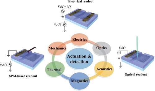
LDMs-based NEMS resonators in resonant structures (single/double-clamped beams and drums) could be linearly or nonlinearly driven by actuation schemes including electrodynamic, electrostatic, thermos-elastic, piezoelectric and optic ones [Citation58,Citation67,Citation68]. The feedbacks of the detection are delivered in terms of electrodynamics, electrostatic (capacitive), piezoresistive, piezoelectrics and optics (Figure ) [Citation69]. In order to optimize the performance of each resonator, distinct dynamical approaches were demonstrated, consisting of (1) activating higher-order modes to improve the sensitivity of mass/gas sensing, (2) multimode activation to simultaneously measure multiple parameters within one single device, (3) internal resonance to improve resonator stability and (4) modal coupling and their implementations in signal processing. Due to the high resonator frequencies, small vibration amplitudes and tiny dimensions of LDMs-based NEMS resonators, the readout in a relatively precise way is challenging. Moreover, the conventional mechanical actuation and detection methods (like modal hammers and accelerometers) are too large or invasive to apply, rendering the superiority of contactless electronic and optical readout and actuation techniques [Citation26,Citation67–71]. In optical methods, optical interference is usually adopted to optically stimulate resonators, record phase shifting and consequently abstract displacements through signal demodulation. During the device-scaling-down process (especially from the micron to nano and even atomic scale), however, the efficiencies of actuation and detection were extremely reduced. To push NEMS resonators a step closer toward terminal performances, transduction techniques including magneto-motive transduction, single-electron transistor detection and sensing, and arbitrary combinations of previously mentioned protocols emerged to eliminate these drawbacks [Citation60].
Figure 3. Potential couplings between mechanical, optical, electrical, magnetic, thermal and acoustics degrees of freedom in NEMS resonators.
2.3 Resonator dynamics
In general, the architecture of LDMs-based NEMS resonators could be mainly classified into four categories: singly-clamped beam, double-clamped beam/film, partially-clamped film and full edge-clamped film [Citation72]. With respect to different device configurations, electromechanical resonators may work with or switch between different modes. Tiny variations in structure might create completely different mechanical characteristics even under the same driving conditions. For instance, a cantilever beam electromechanical resonator may work in torsion, bending, longitudinal expansion and contraction modes [Citation73]. For different vibration modes, multiple higher harmonic oscillation frequencies may generate synchronously or alternatively, exacerbating the urgency of dynamics research.
For 1DMs-based NEMS resonators, the main configurations are cantilever beam and doubly-clamped beam. Taking a doubly-clamped beam as an example, the displacement of vibrating beams in the z-direction is given by [Citation74]
(1)
(1) with ρ is the density, r is the radius, E is Young’s modulus, I is the momenta of inertia, and T is the tension of materials. Assuming that z = ∂z/∂x = 0 at x = 0 and x = L, I = πr4/4 and T = 0, the resonance frequencies are [Citation74,Citation75]
(2)
(2) with wavenumber (β0) and the length (L) of the doubly-clamped beam.
Among numerous 2DMs-based NEMS resonators, the drum configuration (film or membrane) attracts overwhelming attention [Citation76] and therefore the fundamental overview of resonator dynamics will be delivered based on drum configuration here. For vibrations of 2D drum resonators, the flexural rigidity can be formulated as [Citation52,Citation77]
(3)
(3) where Eγ is the 3D modulus, d is the thickness and ν is the Poisson’s ratio of the material. In the meantime, the resonance frequency of resonators can be defined as [Citation52,Citation77,Citation78]
(4)
(4) where k is the modal parameter, r is the radius of the drumhead, ρ is the areal mass density and γ is the membrane pretension. The formula contains three regions: when γr2/D approaches 0, the formula is close to the plate model, whereas, when γr2/D approaches ∞, the formula converges into the membrane model, and in-between these two conditions is the transition model.
In conventional electromechanical resonators, it was claimed that unusual dynamic behaviors such as geometrically nonlinear modes and strong modal coupling [Citation79] exist pervasively under certain scenarios. Taking electrostatic excitation as an example, the resonance of NEMS resonators was mostly linearly under low excitation intensity [Citation80]. However, with increasing intensity of actuation, the resonance curve deformed from symmetrical to unsymmetrical and the resonance peak gradually shifted toward higher frequency (also defined as a hardening-type nonlinear vibration). In this case, the nonlinear vibration of resonators could be represented by Duffing’s equation [Citation81]
(5)
(5) where Meff is the effective mass of harmonic oscillator, γ stands for linear damping related to the quality factor, k0 is the linear stiffness, β is the nonlinear stiffness, x is the displacement field and ˙ ≡ dx/dt (t is the time). The nonlinearity in NEMS resonators mainly originates from four parts: (1) The most obvious source is material nonlinearity. In this system, the relationship between stress and strain becomes nonlinear. For small strains, the stress and strain follow linear Hooke’s law. However, when the strain becomes larger that the critical point, the material undergoes plastic deformation, and the corresponding motion equation is nonlinear [Citation82]. Therefore, nonlinearity is usually observed in extremely rigid or specially designed structures [Citation79]. (2) The second source of nonlinearity might originate from nonlinear dependences on the displacements of excitation force. Under electrostatic excitations, the value of driving force is determined by the dynamic range and magnitude of applied voltage between the resonator and the driving electrode. Consequently, obvious nonlinearity appears. (3) The third origin is the nonlinearity related to geometry and boundary of resonators. For a doubly-clamped beam in bending modes, a non-zero deflection means the effective elongation that can only be achieved by generating longitudinal stress within the beam [Citation83]. At the same time, the longitudinal stress changes the resonance frequency and then introduces nonlinearity to the system. (4) The last source of nonlinearity is nonlinear damping which affects the dissipation of mechanical structures [Citation84].
Nonlinearity in damping exists in many extreme cases and even in the linear response states [Citation85,Citation86]. In addition to linear oscillation, the nonlinear effects in graphene resonators could be described by the Duffing effect with large amplitude. In this aspect, Eriksson et al. [Citation87] reported the frequency tuning, nonlinearity and mode coupling of graphene drum resonators by solving the Airy stress problem. The analytical expressions of eigenfrequency and nonlinear coefficients with radius, suspension height, initial tension, gate voltage and elastic constant were first obtained. The authors further proved that the nonlinear modeling of 2D NEMS resonators must take second and third coefficients of the nonlinear Duffing equation (the quadratic term from bending and defects, and the third term induced by radial in-plane tension increment) into account.
2.4. Figure of merit
2.4.1 Resonance frequency
According to the equipartition theorem, the kinetic energy of mechanical vibration (defined as an eigenmode) is equal to the potential energy stored in vibrational deformation at the intrinsic frequency of an ideal resonating structure [Citation88] At the eigenfrequency, the total energy in the mechanical system endlessly passed back and forth between kinetic and potential energy. In practical, energy dissipation is inevitable in real vibration mechanical systems. The eigenmode mechanism in resonators with inherent energy loss is then noted as resonance. Correspondingly, the frequency exchange between kinetic energy and potential energy is defined as the resonance frequency (f0). The value of f0 is used to estimate the quality of NEMS resonators. Typically, high resonance frequency implies the potential of rapid response to external fluctuations and is indispensable for exploring the quantum phenomena in NEMS resonators.
The dynamics of flexural electromechanical resonators could be modeled as simple damped harmonic oscillators with an effective mass (meff), a spring constant (k), and a mechanical resonance frequency (f0): [Citation6,Citation74,Citation89]
(6)
(6)
It can be seen that high resonance frequency requires one material with large k and small meff values. The LDMs-based NEMS resonators have a high resonant frequency due to extremely small effective mass. At present, the major resonance frequencies of CNTs-based resonators are located in the very-high frequency (VHF) and ultra-high frequency (UHF) range and may stride into the terahertz range with further efforts [Citation18]. In addition to material selection, manufacturing process, [Citation90] working environment [Citation91] and additional quality [Citation92] were also verified to affect the resonant frequency to certain degrees.
2.4.2 Quality factor
Quality factor (Q), defined as the ratio of stored energy and lost energy during resonance (equation 7), is another key parameter to reflect and judge the quality of NEMS resonators [Citation93]
(7)
(7) where W is the total energy stored in the system, ΔW is the lost energy during one oscillation period. By measuring the energy difference between storage and dissipation, the quality factor is a damping indicator of resonators. The most intuitive signature of high Q values is a sharp peak in the resonance spectrum. The origins of energy loss could be mainly divided into three parts: [Citation6] (1) The first is the energy loss from the interaction between the resonator and the medium from working environment. (2) The second one comes from clamping loss induced by the radiation over the NEMS anchors. (3) The last one lies in the inherent damping of materials, such as the interaction between phonons and electrons. The achievement of a high Q value usually reduces the pumping power to maintain device operation and is also beneficial to reduce measurement errors caused by energy loss and other lagging effects. For high precision resonators, outstanding Q values are required to guarantee the accurate frequency selection with minimal energy loss.
According to the energy loss mechanism, device manufacturing process, material properties and the operating temperature are the main factors that affect the Q factor of NEMS resonators. Therefore, there are three main strategies for improving the Q factor [Citation94]. (1) The first method is to diminish the contaminations and surface frictions by optimizing the device manufacturing process. (2) The mechanical quality of harmonic oscillators requires further improvements. For instance, researchers have obtained high-Q NEMS using single-crystal diamond films and high tensile SiN films [Citation75,Citation78,Citation95]. (3) The third method is to cool the operating temperature for resonators. At present, rational engineering of quality factors is essential for NEMS resonators to meet the criterion of sensing, signal processing and quantum physics investigations.
2.5. Tunability and engineering
During the NEMS operations, the resonance frequency needs to match the proposed vibration frequency that heavily relies on the crystal structure and manufacturing process. Therefore, the existence of vacancies and defects embedded in the lattice structure would definitely affect the resonance frequency and tunability. One promising method is to utilize electrostatic gate to tune the natural frequency of NEMS resonators [Citation96]. Alternatively, the tuning of resonance frequency might also be completed by heating and controlling the thickness of resonating materials. For instance, Ye et al. [Citation97] reported the electro-thermal tuning of monolayer and few-layer graphene-based NEMS resonators and demonstrated their steady operations in high and even ultra-high frequency bands. After elegant control of Joule heating, the tunable frequency could be realized via electric heating at 1200 K. In this process, the in-plane tension of single-, bi-, and tri-layer graphene were increased due to the heating-induced shrinkage and thereby the resonance frequencies increased. More importantly, the tuned resonant frequency range of trilayer graphene device even approached ≈ 310%. Moreover, Lee et al. [Citation98] reported that γ-ray radiation could be implemented to tune the resonance frequency of MoS2-based NEMS resonators. Due to the changes induced by ionizing γ-ray, the resonance frequency of as-fabricated device raised after exposure for 24 h and returned to the initial stage once the exposure expired.
In addition to frequency tuning, Q engineering shows equal importance for signal detection and SNR of NEMS resonators. One potential problem is that the reductions of device dimensions usually reduce the Q factor. Although the Q factor increases significantly under cryogenic and vacuum conditions, the indispensable equipment and high expenses limit the propagation of LDMs-based NEMS resonators. Therefore, increasing the Q factor at ambient and room temperature is imperative for the present LDMs-based NEMS resonators. As a complement to the three main strategies discussed in the previous section, Cartamil-Bueno et al. [Citation99] reported a laser oxidation process to improve both the Q factor and resonant frequency of multilayer tantalum oxide (TaSe2) resonators. In virtue of the thermal shrinkage after laser oxidation, the stress in resonators was increased by 8 times. Consequently, enhanced Q factor (14 times) and resonant frequency (9 times) were captured in multilayer TaSe2 resonators.
The materials, dimensions, resonance frequency (f0), effective mass (Meff), and quality factor (Q) for several MEMS/NEMS resonators are summarized in Table . Compared with 2D NEMS, 1D NEMS possess a relatively smaller mass and size that produce better mass response and resolutions together with their ultra-rigid characteristics. Furthermore, the strong electron-vibrational coupling in 1D NEMS provides an ideal platform for probing the quantum limit of motion and manipulating quantum states. While for 2D NEMS resonators, the ultra-high strain limit of 2DMs brings excellent tunability and larger coupling region, beyond the scope of 1D NEMS resonators. In addition, the strain modification in 2DMs and their heterostructure resonators may create pseudomagnetic fields, promising for magnetic nanosensors with ultrahigh sensitivity [Citation100]
Table 1. Resonance frequency (f0), effective mass (Meff) and quality factor (Q) for reported MEMS resonators and LDMs-based NEMS resonators (G for graphene).
3. Low-dimensional materials for NEMS
Attributed to the outstanding mechanical, optical, and electrical properties, LDMs involving CNTs, graphene, h-BN, TMMCs, TMDCs, BP and their vdW heterostructures, have attracted massive attention toward NEMS applications. In recent years, many precise nano-sensors based on CNTs were reported in succession, leading to a series of notable milestones in the field of LDMs-based NEMS resonators. Taking the force and mass sensing as an example, the force and mass sensitivities of CNTs-based NEMS resonators reached up to record values of zN (10−21N) and yg (10−24g) level, respectively. This section aims to discuss the ‘Butterfly’ effect and recent progress of diverse LDMs-based (as shown in Figure ) NEMS resonators. The mechanical and electrical properties of aforementioned LDMs are detailly summarized in Table to offer an insightful database for constructing efficient NEMS devices.
Figure 4. Crystal structures of representative LDMs overviewed in this work, covering CNTs, graphene, h-BN, BP, TMDCs and their heterostructures.
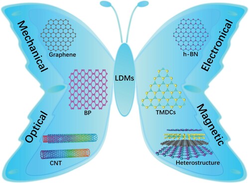
Table 2. Mechanical and electrical properties of several low-dimensional materials.
3.1. CNTs-based NEMS resonators
Carbon nanotubes (CNTs) are one-dimensional carbon materials and could be regarded as curled graphene sheets at a certain angle. In light of layer number of ‘graphite sheet’, CNTs are divided into single walled carbon nanotubes (SWCNTs) and multi walled carbon nanotubes (MWCNTs). Given that SWCNTs and MWCNTs possess apparently different mechanical, electronic and optical properties, distinct performances of SWCNTs and MWCNTs in NEMS resonators might be expected. More importantly, the excellent mechanical strength ( ∼ 1.2 TPa), [Citation101] mass density (ρ ∼ 1.7 g/cm3) [Citation102] and electrical conductivity (mobility ∼ 105 cm2/(V·s)) [Citation103] of CNTs well satisfy the essential qualifications of premium NEMS resonators, stimulating several milestones in the community of CNTs-based NEMS resonators.
3.1.1 Evolution of CNTs-based resonators
In 1999, by attaching a CNT fiber to a gold wire on an insulator, Poncharal et al. [Citation104] pioneered the single-clamped (cantilever) CNT resonator and stimulated intense research of CNTs-based NEMS resonators. Afterwards, Sazonova et al. [Citation105] proposed the electrical actuation and detection of doubly-clamped CNTs-based NEMS resonators. In other words, both the tension tuning of CNTs and the records of resonance frequency were accomplished by electric fields. This demonstration of outstanding sensitivity, frequency and tunability broadens versatile applications of CNTs-based NEMS resonators. For instance, the exceptional electron transport behaviors including ballistic conduction over long distances and multiple Coulomb blockade-related phenomena, were reported in CNTs-based resonators. Lassagne et al. [Citation106] found the electromechanical coupling in CNTs manifested the nonlinearity of resonator dynamics at cryogenic temperature that electrons entered the Coulomb-blockade regime. Recently, Bai et al. [Citation107] fabricated centimeter-long CNTs using CVD method and showed the fatigue behavior of individual CNTs via acoustic excitations. Nowadays, CNTs-based NEMS resonators also grow to be an ideal platform for studying nonlinear phenomena, quantum electron transport, surface science and light–matter interactions. Next, we attempted to overview the progress of CNTs-based NEMS resonators, especially the breakthrough in last five years.
3.1.2 Actuations and detections
With devices down-scaling to nano-meter level, the excitation and detection of CNTs-based NEMS resonators become quite challenging. At the initial stage, field emission and SEM were first adopted to detect the resonances of CNTs beams, but the unsatisfying sensitivity hindered further NEMS advancements based on CNTs. To surmount these problems, Sazonova et al. [Citation105] reported a tunable CNTs-based NEMS resonator by electrical actuations and detections (Figure (a)). The resonance beam was made of doubly-clamped CNTs with a diameter and length of ∼4 nm and ∼1 µm, respectively. A gate electrode was employed to electrostatically interact with CNTs. The gate voltage (Vg) can induce charges along the CNTs given by:
(8)
(8) where Cg is the capacitance between CNTs and the gate electrode. The attraction between separated charge +q and −q creates an electrostatic force on CNTs. If a DC and an alternating current (AC) are applied to the gate, the total electrostatic force is given by
(9)
(9) where
is the capacitance derivative of the gate with respect to the distance between CNTs and gate,
,
are the DC and AC voltages. Once DC voltage was applied, the length of CNTs varied and consequently the tension along nanotubes altered, leading to a tunable resonance frequency. Moreover, an additional AC voltage was used (Figure (b)) for resonance excitations by generating a periodic driving force. In addition, a gate driving RF signal (frequency ω) was adopted to ignite the resonance process and a carrier signal of frequency ω + Δω was incorporated into the power source. Therefore, the CNT behaved as a signal-mixer and the current variations within the circuits were monitored by a lock-in amplifier. After matching the excited resonance to the resonance frequency of CNTs by adjusting the RF signal, sharp variation occurred in both the amplitude and phase of the as-generated current. Conductance variations along CNTs directions were revealed to be proportional to the induced charge fluctuations while the vibrating detection was recorded by measuring conductance variations between resonant structure and substrate electrode. Using this method, the authors proved the effectiveness of DC gate voltage in adjusting the CNT tension and the resonance frequency (Figure (c)). It is also worth highlighting that all the processes here were conducted with sole electrical means [Citation105]. Although the experimental setup, actuation and detection are simple, it remains difficult to distinguish each resonance peak from the circuit. Under this dilemma, Garcia-Sanchez et al. [Citation108] proposed an integrated method to detect the mechanical motion of CNTs resonators by a scanning force microscopy (SFM) cantilever. As shown in Figure (d), an oscillating voltage was applied through the gate to actuate the motions of CNTs. The mechanical vibrations were probed by modulating the oscillating frequency of the applied voltage by a side gate electrode to match first eigenmode of the SFM cantilever (Figure (e)). To minimize the force exerted on the tube by the SFM cantilever, the tapping working mode was selected throughout the whole measurement. The superiority of this method rested in the spatial resolution of CNT resonance and the direct imaging of resonance mode. Recently, Bonis et al. [Citation109] proposed an ultrasensitive detection scheme to reduce the noise limit in detecting vibrations, which utilized a resistor-inductor-capacitor and a high electron mobility transistor amplifier (Figure (g)) at liquid helium temperature. By reducing SNR of thermal vibrations to 17 dB at 300 mK, the displacement and force sensitivity of the device (Figure (h)) could reach up to 0.5
and 4.3
, respectively. From the views of prime cost and accessibility, electrical or optical means are frequently preferred to drive and detect NEMS resonators up to date.
Figure 5. Representative actuations and detections of doubly-clamped CNTs resonators. (a) A false-color SEM image of a suspended device (top) and corresponding schematic (bottom). (b) The experimental setup. (c) Color plots of current response vs Vg and driving frequency [Citation105]. The inset shows the extracted peak positions in the frequency-gate voltage map. (d, e) SEM image and schematic of a CNTs resonator device. (f) Topography (i) and bending-mode nanotube vibration (ii-iv) images at different actuation frequencies. Zero (ii), one (iii), and two (iv) nodes correspond to first, second and third-order bending eigenmodes, respectively [Citation108] (g) Schematic of CNTs vibration measurement using an RLC resonator and a low-temperature HEMT amplifier. (h) The fundamental eigenmode displacement noise spectrum of CNTs resonators [Citation109].
![Figure 5. Representative actuations and detections of doubly-clamped CNTs resonators. (a) A false-color SEM image of a suspended device (top) and corresponding schematic (bottom). (b) The experimental setup. (c) Color plots of current response vs Vg and driving frequency [Citation105]. The inset shows the extracted peak positions in the frequency-gate voltage map. (d, e) SEM image and schematic of a CNTs resonator device. (f) Topography (i) and bending-mode nanotube vibration (ii-iv) images at different actuation frequencies. Zero (ii), one (iii), and two (iv) nodes correspond to first, second and third-order bending eigenmodes, respectively [Citation108] (g) Schematic of CNTs vibration measurement using an RLC resonator and a low-temperature HEMT amplifier. (h) The fundamental eigenmode displacement noise spectrum of CNTs resonators [Citation109].](/cms/asset/b67cbc82-5e68-4992-9d57-279df725d5e5/tmrl_a_2111233_f0005_oc.jpg)
3.1.3 Figure of merit
NEMS resonators with ultra-high frequency not only show great potential for mass and force sensitivity, but also offer exceptional systems for exploring quantum phenomena. For the sake of achieving ultrahigh resonance frequencies, the modes of mechanical motion in the lowest quantum states were quite promising [Citation110–112]. To improve resonance frequency, many efforts were devoted to optimizing detection methods, device architectures and manufacturing processes. For instance, through optimizing the detections by introducing mixing technology, Sazonova et al. [Citation105] demonstrated the frequency of ∼ 200 MHz in a double-clamped CNTs device in vacuum (<10−4 torr). Afterwards, Peng et al. [Citation18] further employed metal nanobridge coatings and the frequency of fundamental mode of CNT-based NEMS resonators was recorded to exceed 1.3 GHz at room temperature in air. Recently, Laird et al. [Citation113] reported a resonance frequency of 39 GHz in a doubly-clamped CNT electromechanical resonator (at 100 mK, in dilution refrigeration), the highest reported resonance frequency of CNT resonators so far. The authors attributed this phenomenon to a thermally excited state probability below 10−8 and a relaxation time of 140 ns by cooling the resonator into ground states. In addition, the shrunk CNT resonator with suitable coating materials (such as Fe) achieved resonance frequencies more than 10 GHz or even into the THz range [Citation18]. In a nutshell, with suitable coating materials and CNT shrinking, the resonance frequency of CNTs-based devices set a record value, but further efforts are still demanded to impetus ultrahigh frequency from laboratory to practical scene.
Quality factor that reflects the detection accuracy and energy loss is another perpetual index for CNTs-based NEMS resonators. So far, the methods to improve the Q factor mainly focus on growing ultra-clean CNTs and lowering the working temperature in vacuum conditions [Citation114]. On one hand, the employment of ultra-clean CNTs certainly reduces the surface friction for achieving a higher Q factor, concurrently improving the operation stability of as-fabricated devices. On the other hand, cooling the resonator to millikelvin (mK) temperature in a vacuumed cryostat would reduce ‘pollution’ (surface adsorption) [Citation115] and consequently enhance the Q factor. Moser et al. [Citation94] tested an ultra-clean nanotube resonator at 30 mK and achieved a Q factor up to 5 × 10⁶, the highest Q value so far (Q ∼ 1.4 × 10⁴, at 6 K [Citation113]). Apart from the optimized process and low-temperature operation, the accomplishment of higher Q value might reside in further improvement of measurement technologies to minimize the impact of electrostatic noise.
3.1.4 Devices physics
The aspiration of higher quality factor drives researchers to explore possible origins of energy dissipation (Q−1) during operations. Among diverse assumptions, air damping plays a dominant role in dissipation since gas molecules inevitably surround the resonators. Energy wastes from the interactions between vibrating structures and surrounding air molecules. For a long time, damping in the Foucault pendulum and submicron NEMS resonators can be described by a linear damping force γdx/dt (γ is the relevant damping coefficient, x is the deflection of the resonator and t is the time). After implementing LDMs, it becomes possible to explore damping in more than one atomic systems. Eichler et al. [Citation116] studied the damping of NEMS resonators based on CNTs and graphene sheets. In their resonators, the linear damping model failed to describe and the damping behavior became nonlinear. But after introducing a coefficient (η) of nonlinear damping, the damping of CNT and even graphene NEMS resonators could be well explained by a nonlinear damping force (ηx2dx/dt). In addition, they also pointed out the strong dependence between damping and vibration amplitudes. Though nonlinear characteristics of damping may offer some clues to improve the overall performances, further damping study is conducive to a deeper understanding of energy dissipation and tunable quality factors in CNTs-based NEMS resonators.
Although the quantum states were observed and manipulated in CNTs-based NEMS resonators, the possibility of observing quantum effects is diluted by the thermal noise force. Therefore, efficient methods to cool these systems into the quantum regime were highly required. Principally, the back-action of electrons on the resonator might suppress thermal vibrational fluctuations. After integrating a RF resonator with a superconducting single-electron transistor, Naik et al. [Citation117] achieved a population number of 200 quanta far from the quantum regime. On this basis, Urgell et al. [Citation118] later demonstrated the back-action of electrons on resonator vibrations as a simple and efficient method to cool the resonators to the quantum state limit. To minimize the residual contaminations, CNTs were directly grown between two electrodes by CVD methods (Figure (a)). After being inserted into a dilution refrigerator, the resonator was cooled to 70 mK and then a DC current was applied to modulate the dynamics of vibrations. These modified vibrations reacted with electrons and formed a closed-loop with finite delay. The reaction significantly reduced thermal vibrational fluctuations and as-generated self-oscillations (Figure (b)) lowered the device vibration to 4.6 ± 2.0 quanta (Figure (c)). This protocol suggested that electrons would be a powerful resource for quantum manipulations in NEMS resonators. As shown in Figure (d), Deng et al. [Citation119] reported a CNT resonator coupled with two independent tunable modules. The frequency of each resonator was separately tuned by two local gates. Moreover, the conductance of each resonator was uniformly modulated by one additional resonator between two resonators through phonon–phonon interactions. The electron fluctuation in CNT induced the back-action force on the mechanical modes while softened and even damped the phonon modes. As a result, the coupling strength of two series-connected CNT resonators was found to reach more than 200 kHz, providing opportunities to probe electron–phonon coherent interactions, electron long-range coupling and electron entanglement states.
Figure 6. Additional physics in CNTs-based resonators. (a) Schematic diagram of a CNT device (top) and relevant SEM image (bottom). (b) as function of Vsd. The yellow shaded area represents the region with self-oscillation of the device. (c) Sz vs Δω/2π curve recorded at Vsd = 0.565 mV [Citation118]. (d) Strongly-coupled CNTs resonators. Schematic diagram (left) and color mapping (middle) of the coupled resonator and double quantum dot system as a function of driving frequency and DC voltage (right) [Citation119]. (e) The acoustic resonance setup for investigating the vibration behavior of centimeter-long individual CNTs [Citation107].
![Figure 6. Additional physics in CNTs-based resonators. (a) Schematic diagram of a CNT device (top) and relevant SEM image (bottom). (b) δz2 as function of Vsd. The yellow shaded area represents the region with self-oscillation of the device. (c) Sz vs Δω/2π curve recorded at Vsd = 0.565 mV [Citation118]. (d) Strongly-coupled CNTs resonators. Schematic diagram (left) and color mapping (middle) of the coupled resonator and double quantum dot system as a function of driving frequency and DC voltage (right) [Citation119]. (e) The acoustic resonance setup for investigating the vibration behavior of centimeter-long individual CNTs [Citation107].](/cms/asset/d77e142a-9eff-41f4-9382-9557b0a3bfc0/tmrl_a_2111233_f0006_oc.jpg)
Recent studies demonstrated that the combination of optic and acoustic means enables non-destructive actuation and detection of resonances in CNTs-based devices. As shown in Figure (e), the author deposited TiO2 nanoparticles onto CNTs for optical visualization and frequency tuning and further claimed robust tuning effects by controlling the density of particles. Different from traditional e-beam-related characterizations, this non-contact measurement by an optical microscope avoided damaging CNTs by high-energy electron beams, and simultaneously realized the detections of centimeter-long individual CNTs in air. To date, ultra-small geometry, tunable frequency, high quality factor and sensitivity were achieved in CNTs-based NEMS resonators and many innovative sensors were demonstrated in succession. However, the atomic structures of CNTs have a negative impact on device repeatability, and the dynamics and reliability of the CNTs resonators are immature. Next, the combinations of experiments and finite element simulations may be the perspective direction for CNTs resonators. An in-depth understanding of the working mechanisms simultaneously provides valuable guidance for designing and developing novel NEMS resonators.
3.2 Graphene-based NEMS
Graphene, sp2 carbon atoms closely packed into a honeycomb structure, exhibits excellent mechanical and electrical properties that are qualified for high-performance NEMS resonators [Citation78]. For instance, benefiting from Young’s modulus up to 1 TPa, breaking strength of 130 GPa and the strain tolerance up to 25%, [Citation25] graphene-based NEMS resonators achieved resonance frequencies as high as 178 MHz [Citation64] and quality factors up to 100,000 at 100 mK [Citation116]. These peculiar properties and outstanding performances render graphene one of the most studied 2DMs for NEMS resonators.
3.2.1 Evolution of graphene-based NEMS resonators
With the mature preparation methods (mechanical exfoliation and CVD methods), significant advances in versatile graphene-based NEMS resonators have been achieved and the aforementioned superior properties of graphene were fully utilized in resontors [Citation120]. The first-generation graphene NEMS resonators were prepared on graphene from mechanical exfoliation in 2007 [Citation121]. Subsequently, Van der Zande et al. [Citation199] fabricated large arrays of suspended CVD graphene resonators with different configurations. Under optical/electrical actuation and detection, the NEMS resonators based on CVD graphene exhibited comparable electromechanical properties with graphene devices from mechanical exfoliation. Furthermore, Chen et al. [Citation96] applied simple circuits to enable graphene oscillators to generate and convert self-sustaining mechanical motion at room temperature. Then, the frequency modulation and signal generation efficiently realized the transmission of audio signals. With remarkable mechanical, electronic, optical and phononic properties, graphene is also advantageous to probe the coupling between fundamental excitations and macroscopic mechanical modes. For instance, by introducing bending vibrations in graphene, Zhang et al. [Citation122] took advantage of the micro-Raman spectroscopy to illustrate the dynamic of optical phonon softening. This work also highlighted the importance of dynamic strain engineering and dynamic strain-mediated control of light–matter interactions in 2D materials and their heterostructures. Moreover, by adjusting the excitation power to achieve a continuous two-to-one resonance, Keskekler et al. tuned the parametric resonance of graphene device in the range of 40–70 MHz and reported a nearly twofold increment of nonlinear damping [Citation123]. In this section, we summarized the working mechanisms, actuation and detections, key indices and recent progress of graphene-based NEMS resonators.
3.2.2 Actuations and detections
Similar to CNTs-based NEMS resonators, the excitation methods for igniting graphene resonators are mainly optical and electric means. For optical excitation, a laser with periodical intensity was irradiated onto suspended graphene and then absorbed heat with expansion excites the vibrations of graphene. On the contrary, the electrical excitation is usually applied to graphene devices with a field-effect transistor (FET) structure. Conducting substrates are employed as back gates and a pair of source and drain electrodes are fabricated for imposing AC and DC signals. Modulated by the electrostatic force between graphene and the back gate, the vibration of graphene begin to ignite and the resonance frequency is highly correlated with the amplitude of DC voltage.
The detections for graphene vibrations are similarly divided into optical and electrical detections. Optical detection is achieved in light of optical interference principle. For graphene on a silicon wafer device, suspended graphene forms a Fabry–Perot cavity with the ‘hollow’ silicon substrates. Once irradiated to the graphene surface, the laser beam is split into two beams: one beam directly reflected by graphene film, and another beam transmitted through graphene and then reflected by the bottom surfaces. The reflected beams of different optical paths interfere with each other, and the interfered amplitude reflects the vibration strength of graphene. Finally, a photodetector is used to convert interference information into electrical signals and then the detection process is completed by a spectrum analyzer. In this detection mode, the tension and vibration information of graphene can be abstracted by measuring the conductance and using the relationship between conductance and internal stress of graphene. For example, Barton et al. [Citation53] studied the behaviors of graphene-based resonators using electrical excitation and optical detection (Figure (a)). Under a low-power laser (300 µW), vibration amplitude of suspended graphene (square shape) was measured as functions of frequency and gate voltage (Figure (b)). The frequency vs Vg curves were also plotted to extract the density of the resonant cavity [Citation124]. At lower laser power, graphene vibrates in light of Brownian motion. With increasing the laser power, the vibration amplitude of graphene increased monotonically and finally approached its natural regeneration and self-oscillation stage. As shown in Figure (c), self-oscillation (in frequency) of graphene films could be elegantly tuned by gate voltages.
Figure 7. Graphene-based NEMS resonators manipulated by optical, acoustic and thermal approaches. (a) Experimental setup of graphene resonators by capacitive driving and optical monitoring [Citation53]. (b) 2D mapping of amplitude of reflected lights vs frequency and Vg at low laser power (300 µW) [Citation53]. (c) Log-scale amplitude vs frequency and Vg, showing the tunable frequency when graphene is self-oscillating [Citation53]. (d) A false-color SEM image of graphene-based resonator. (e) Schematic diagram of actuation and detection for graphene resonators. Ultrasonic waves propagate through the substrate to gold contacts and actuate the graphene resonator, thereby generating an electrical signal [Citation125]. (f) False-color SEM image of graphene device. Graphene sheet (blue) is suspended from the AuPd (yellow) heater and supported by surrounding AuPd islands. (g) The measured resistances as functions of heating voltages. (h) Frequency versus quality factor plot at different heating voltages [Citation126].
![Figure 7. Graphene-based NEMS resonators manipulated by optical, acoustic and thermal approaches. (a) Experimental setup of graphene resonators by capacitive driving and optical monitoring [Citation53]. (b) 2D mapping of amplitude of reflected lights vs frequency and Vg at low laser power (300 µW) [Citation53]. (c) Log-scale amplitude vs frequency and Vg, showing the tunable frequency when graphene is self-oscillating [Citation53]. (d) A false-color SEM image of graphene-based resonator. (e) Schematic diagram of actuation and detection for graphene resonators. Ultrasonic waves propagate through the substrate to gold contacts and actuate the graphene resonator, thereby generating an electrical signal [Citation125]. (f) False-color SEM image of graphene device. Graphene sheet (blue) is suspended from the AuPd (yellow) heater and supported by surrounding AuPd islands. (g) The measured resistances as functions of heating voltages. (h) Frequency versus quality factor plot at different heating voltages [Citation126].](/cms/asset/e32fc51a-7603-42e4-a4e1-2d1debd29774/tmrl_a_2111233_f0007_oc.jpg)
In addition to electrical and optical methods, recent studies have introduced acoustic and thermal means into actuating and detecting graphene-based NEMS resonators. Verbiest et al. [Citation125] successfully actuated a rectangular graphene resonator by using the substrates to transmit ultrasonic waves (Figure (d)). In addition to the standard capacitive actuation, a piezoelectric element with a resonance frequency of 4.5 MHz was employed to mechanically vibrate the substrate. Figure (e) shows the actuation of graphene resonator by introducing ultrasound. Due to the high nonlinearity of the mechanical restoring force, ultrasonic waves could be reflected by the resonance frequency shift. In this study, graphene resonators were found to detect ultrasonic vibrations in a frequency range from 1 to 100 MHz. Hence, the integration of graphene resonators onto the backside of AFM cantilevers would enable ultrasonic detections of arbitrary substrates and surfaces with high sensitivity. This scheme is applicable to drive other 2DMs-based NEMS resonators and even non-conductive resonators. Davidovikj et al. [Citation126] subsequently proposed a chip-scale heating device (Figure (f)) to modulate the in-plane tension of suspended graphene. Using the theory of DC Joule heating, graphene NEMS resonators were electro-thermally driven and in-plane tension of suspended graphene was tuned on demand, leading the increment of the resonant frequency by 10%. For calibration purposes, a thermal treatment was conducted and the resistance vs heating voltage curve was shown in Figure (g). In the presence of corrugations, relaxations, and wrinkles, the thermal expansion from the heater generated an out-of-plane force component and excited the motion of the graphene drum. In contrast to electrostatic force tuning, thermal tuning was able to produce 32% increment in the quality factor due to the enhanced in-plane tension (Figure (h)). Therefore, the resonant frequencies and quality factors may be tuned separately in graphene-based NEMS devices, toward next-generation RF filters, modulators and oscillators.
3.2.3 Figure of merit
Due to the higher effective mass (effective mass MG/MCNT ≈ 106) and lower spring constant of graphene, [Citation53,Citation127] the resonant frequency of graphene-based NEMS resonators mostly lies in the MHz frequency band, slightly lower than that of CNTs-based resonators. In the resonator made of bilaterally fixed monolayer graphene (L × W, 1.1 × 1.93 µm2), Bunch et al. first reported the resonance frequency device to be 70.5 MHz in vacuum (< 10−6 torr) and at room temperature [Citation121]. Later, Chen et al. [Citation96] developed a monolayer graphene (1.1 × 3.3 µm2) NEMS resonator and confirmed that both resonance frequency and quality factor increased monotonically with decreasing the operating temperature. In addition, additional mass and grid voltage also affected the resonant frequency of graphene. Recently, Jung et al. [Citation128] designed a NEMS resonator with a rectangle (3 × 1 µm2) graphene p-n junction and reported the resonance frequency up to 1.17 GHz after cleaning graphene by current annealing. The remarkable resonance frequency was ascribed to the low mass and high tension (∼ 4%) of graphene. However, several factors including pre-stress and additional mass elevate the difficulty of recording graphene resonance accurately. In addition, imperfections and contaminations from fabrication and test procedure residue in graphene plane in a massive and random fashion and severely lowered the resonance frequency.
Apart from the resonance frequency, another biggest obstacle in graphene-based NEMS resonators is the inadequate quality factor. The quality factor is concluded to closely correlate to graphene sizes, working temperature and boundary conditions. Date back to the initial stage, the highest quality factor observed in monolayer graphene resonators was only a few hundred at room temperature [Citation120,Citation199]. Later, Robinson et al. [Citation129] manufactured NEMS resonators from large-area and few-layer reduced graphene oxide (rGO) films (Figure (a)) and achieved a quality factor of 4000. Compared to intrinsic graphene, additional chemical bonds in rGO films improved their ability to undergo in-plane tension (up to 5 N/m) and afterward the value of quality factor. Moreover, Zalalutdinov et al. [Citation130] reconfirmed that Young’s modulus (up to 800 GPa) and strength (sustainable stress 1 GPa) of chemically modified graphene (CMG) films were dramatically improved by introducing carbon–carbon bonding. Consequently, a RF nanomechanical resonator based on CMG films showed a quality factor of 31,000 at room temperature (Figure (b)). Meanwhile, these attempts overcame the difficulties in synthesizing and manipulating large-area and ultra-thin films for massive NEMS productions. In accordance to their reports, the resonant frequency and quality factor could be further increased by adjusting internal stress in graphene films. However, in-depth understanding and efficient metrologies to push the quality factors of graphene resonators to higher-order remain desirable.
Figure 8. Modifications and integrations of graphene-based NEMS resonators. (a) rGO films on pre-patterned substrates. SEM images show (i) 20 nm and (ii) 4 nm thick rGO films suspended on Si pillars beds. (iii) Optical image of 3 × 3 rGO drum arrays. (iv) AFM height image of an intact drum resonator. The suspended film is approximately 10 nm below the top SiO2 surface. (v) SEM image of a drum resonator milled with a micro-hole [Citation129]. (b) Mechanical engineering of ultrathin CMG films through chemical modifications (stiffness, strength, density, and built-in stress) [Citation130]. (c) Schematic of a graphene-SiNx hybrid resonator [Citation132]. (d) Giant nonlinear response of graphene-SiNx modes after coupling graphene and SiNx resonators. (e) Coherent frequency combs of new frequency components arisen from both graphene and SiNx hybrid modes above the threshold of pump voltage. (f) Illustration of the photo-tuning effect in 2D NEMS resonators [Citation134]. (g) Resonance spectra after partial light doping at different Veff. The amplitude changes due to different conduction and driving efficiencies.
![Figure 8. Modifications and integrations of graphene-based NEMS resonators. (a) rGO films on pre-patterned substrates. SEM images show (i) 20 nm and (ii) 4 nm thick rGO films suspended on Si pillars beds. (iii) Optical image of 3 × 3 rGO drum arrays. (iv) AFM height image of an intact drum resonator. The suspended film is approximately 10 nm below the top SiO2 surface. (v) SEM image of a drum resonator milled with a micro-hole [Citation129]. (b) Mechanical engineering of ultrathin CMG films through chemical modifications (stiffness, strength, density, and built-in stress) [Citation130]. (c) Schematic of a graphene-SiNx hybrid resonator [Citation132]. (d) Giant nonlinear response of graphene-SiNx modes after coupling graphene and SiNx resonators. (e) Coherent frequency combs of new frequency components arisen from both graphene and SiNx hybrid modes above the threshold of pump voltage. (f) Illustration of the photo-tuning effect in 2D NEMS resonators [Citation134]. (g) Resonance spectra after partial light doping at different Veff. The amplitude changes due to different conduction and driving efficiencies.](/cms/asset/0f68dff5-f6b6-4233-8bb1-4dca887c3e40/tmrl_a_2111233_f0008_oc.jpg)
3.2.4 Devices physics
With high resonant frequency and excellent electrical sustainability, graphene-based NEMS resonators are widely adopted in cavity opto-mechanics and nonlinear physics, especially Duffing nonlinearity and nonlinear damping. In these devices, energy from an external pump is essential for parametric amplification to enhance the transmitted mechanical signal. Su et al. [Citation131] demonstrated parametric amplification of a double-clamped graphene resonator by external microwave pumping at doubling the resonant frequency. The extracted nonlinear Duffing force coefficient α and nonlinear damping coefficient η varied with the external pump power, suggesting the influence of higher-order nonlinearity beyond van der Pol and Duffing
in the device. With the increase of pump power, the parametric gain increased and gradually became saturated. In addition, gate voltages were also found to tune the parametric gain (with a maximum gain of 10). In the aspect of nonlinear damping, the microscopic theory of mechanical dissipation shows that nonlinear dampings of resonant modes become greatly enhanced when the resonant mode is connected to a vibration mode close to its twofold resonant frequency. Keskekler et al. [Citation123] investigated the tunability of nonlinear damping in graphene resonators, in which fundamental modes interact with higher modes by parametric drive. By tuning the excitation power, the parametric resonance of graphene drum was tuned in the range of 40–70 MHz to achieve a continuous two-to-one internal resonance and a nearly twofold increment in nonlinear damping. The engineering of nonlinear dissipation in terms of modal interactions and parametric resonances over a wide frequency range contributes to the nonlinear dynamic studies of NEMS resonators.
The integration of various NEMS resonators provides fruitful and tunable oscillatory dynamics and therefore has great potential in both fundamental research and practical devices. For instance, Singh et al. [Citation132] demonstrated an integrated NEMS resonator, consisting of monolayer graphene deposited on the circular hole of a large-area SiNx resonator (Figure (c)). The mechanical mode of graphene resonator was electrostatically tuned to resonate with the SiNx mechanical mode. The resulting mode mixture under the external force produced a prominent nonlinear response (Figure (d)) and delivered a Duffing constant 8 orders of magnitude higher than that of bare graphene resonators. Furthermore, by parametrically driving the coupled modes, a new phonon frequency comb was observed as shown in Figure (e). Afterwards, Verbiest et al. [Citation133] integrated a suspended graphene with a physically- separated comb driver. By attracting graphene electrostatically by a voltage, the coupling strength of graphene resonators could be tuned from 20 kHz to 100 kHz, nearly 1000 times larger than that of bare graphene-based NEMS resonators. These hybrid devices provide powerful platforms for precisely measuring and controlling mechanical mode interactions of LDMs-based NEMS resonators in both the classical and quantum domains even at room temperature.
With the continuous development of manufacturing processes, large-scale resonator arrays stand out in information processing technology and mass spectrometry as the ultralow-loss alternatives to traditional analog electronics. However, an obstacle limiting the widespread adoption of NEMS arrays is the lack of feasible frequency-tuning methods for persistent operation and reversibility. In response to this difficulty, Miller et al. [Citation134] proposed an electro-optical tuning method in graphene-based resonators by the traditional electrostatic gating and optical doping, as shown in Figure (f). The suspended graphene became tightened after gating and the corresponding resonance frequency was manifested through local photo-ionization charges. More importantly, the tuned frequency state remained unchanged for several days in the absence of any external power supply (Figure (g)). Moreover, high-precision repetitive writing and erasing at different resonant frequencies become accessible and in turn enables programming in 2D NEMS resonator arrays. The simulation of complex networks exhibits promising implications for re-programmable phononic crystals and waveguides, as well as nano-mechanical logics and neuromorphic computing.
3.3 TMDCs-based NEMS
With the expanding family of 2D materials, TMDCs (MoS2, WSe2 and etc) have gradually come to the fore and be regarded as active materials for NEMS devices. Different from graphene, TMDCs have distinct semiconducting properties (bandgap ranging from 1.5 to 3.0 eV), rapid response and high sensitivity to external stimulations including light irradiation, magnetic and mechanical forces, thereby becoming the rising hotspot in NEMS resonators in recent years.
Figure (a) illustrates one TMDCs-based NEMS resonator driven by a DC and AC capacitor and measured by optical interferometry [Citation62]. It was found that the quality factor of monolayer WSe2 resonator reached 47,000 at liquid helium temperature, better than monolayer graphene-based resonator with the same surface area and measurement environments. The outstanding Q factor was highly attributed to the low-temperature surroundings that significantly suppressed the thermal contraction of WSe2 lattice. Similarly, a NEMS resonator was fabricated by mechanically peeling MoS2 onto a preset circular hole (diameter of 5.6 µm) and Figure (b) shows the thermo-mechanical resonance spectrum and a sharp resonance peak appeared at 19.68 MHz with a quality factor up to 710 [Citation77]. Furthermore, the resonance mechanisms were further investigated by varying thicknesses and lateral dimensions of MoS2 film. According to their study, these devices were divided into three working areas (Figure (c)), namely, plate limit, transition regime and film limit. A thicker device (10–12 layers) worked in the plate limit and resonant frequency was determined by the geometric size of active flake. While for a thinner device (3–4 layers), the resonator worked in the transition regime and the resonant frequency was highly correlated with the film tension. Castellanos-Gomez et al. [Citation58] further confirmed this film-to-plate transition mechanism by analyzing higher eigenmodes of mono-layer and nine-layer MoS2 resonators. According to the observed resonance spectrum, the eigenmodes of monolayer and multilayer devices were well matched with the theoretical eigenmodes of films and plates, respectively. The elaboration of film-to-plate transition mechanism provided a quantitative guidance and scaling law for next-generation NEMS resonators. Toward massive productions, Jia et al. [Citation185] developed water-assisted lift-off and dry transfer technology and realized the fabrications of suspended CVD MoS2 resonators in large-scale arrays. This simple and convenient method not only avoided chemical pollution but also showed high applicability to all 2D crystals, especially those that are chemically inert to deionized water. To probe the dispersions of fundamental modes, the measured values of f0 and Q were compared with that of mechanically exfoliated MoS2 resonators [Citation57] and even suspended CVD graphene resonator arrays [Citation170]. After normalization, the devices with monolayer CVD MoS2 film (Figure (e,f)) showed the lowest dispersion (44.3%), revealing high uniformity of frequency and quality factor.
Figure 9. Representative NEMS resonators based on distinct TMDCs. (a) Experimental setup of monolayer WSe2 NEMS resonators [Citation62]. (b) Thermo-mechanical resonance of a MoS2 mechanical resonator (solid curve) and the fit via a finite-Q harmonic resonator model (dashed curve) [Citation77]. (c) The relationship between resonance frequency, thickness and layer number of a circular resonator [Citation77]. (d) Mechanical resonance spectra of single-layer (upper panel) and nine layers (bottom panel) MoS2 resonators. For single-layer devices, higher modes appear at frequencies corresponding to circular membranes; while for the thicker resonator, the resonance spectra agree well with the mode of circular plates [Citation57]. (e, f) Comparisons of fundamental-mode resonance frequency (f0) and Q factor dispersions [Citation200]. (g, h) Gate tuning of optically- and electrically-driven resonance in a bilayer MoS2 resonator. Colored dots represent peak amplitudes (their projections onto different planes) under different Vg values [Citation70]. (i) Nonlinear resonance of a single-layer MoS2 resonator [Citation57].
![Figure 9. Representative NEMS resonators based on distinct TMDCs. (a) Experimental setup of monolayer WSe2 NEMS resonators [Citation62]. (b) Thermo-mechanical resonance of a MoS2 mechanical resonator (solid curve) and the fit via a finite-Q harmonic resonator model (dashed curve) [Citation77]. (c) The relationship between resonance frequency, thickness and layer number of a circular resonator [Citation77]. (d) Mechanical resonance spectra of single-layer (upper panel) and nine layers (bottom panel) MoS2 resonators. For single-layer devices, higher modes appear at frequencies corresponding to circular membranes; while for the thicker resonator, the resonance spectra agree well with the mode of circular plates [Citation57]. (e, f) Comparisons of fundamental-mode resonance frequency (f0) and Q factor dispersions [Citation200]. (g, h) Gate tuning of optically- and electrically-driven resonance in a bilayer MoS2 resonator. Colored dots represent peak amplitudes (their projections onto different planes) under different Vg values [Citation70]. (i) Nonlinear resonance of a single-layer MoS2 resonator [Citation57].](/cms/asset/fb2365ac-1968-4708-be82-b1f2e840cf1f/tmrl_a_2111233_f0009_oc.jpg)
To explore the dissipation origin of MoS2 resonators, Lee et al. [Citation135] experimentally developed a batch of devices with different sizes and geometries. Experimentally, it was verified that the dissipation heavily came from the existence of air damping. Moreover, distinguishing from bulk materials, ultra-small effective mass, high surface-to-volume ratio and strain tenability helped 2DMs-based NEMS breaking the power-law dependence with pressure (Q p−1, Q
p−1/2) [Citation95]. From the resonance data, the accumulated tension from the bulging process of MoS2 resonators and the compression cavity enhancements could be clearly identified. Furthermore, the air damping performance was demonstrated to be tunable by changing the film thickness in a precise way. More importantly, this research revealed the possibility of developing different pressure dependencies in 2DMs-based NEMS for tunable resonators, pressure sensing, acoustic wave detecting, and ultrasound imaging. In a parallel study, Lee et al. [Citation70] studied the dynamic range of gridded MoS2 resonators under optical and electrical excitations. The peak amplitude of resonance was found to evolve linearly with Vg (Figure (h)) under electrical excitation, while became related to (Vg)2 (Figure (g)) under optical excitation. These MoS2-based devices further showed a wider dynamic range (up to 70 ∼ 110 dB), surpassing CNTs-based ones for sensing technologies. In a monolayer MoS2 resonator (Figure (i)), a nonlinear behavior with a robust signature was also reported excited by optical power [Citation99]. At low-power irradiation regime, the harmonic oscillation was excited and a clear deviation of harmonic response elevated as a function of increased power. At the critical point (driving power > −9 dBm), the alternation of the stretching tension induced a restoring force and consequently strengthened the frequency response. This observation of nonlinearity offered researchers a starting point for probing the nonlinear dynamics of LDMs-based NEMS resonators, especially those that couple mechanical vibrations with 2D excitons, valley pseudo-spins and single quantum optomechanics [Citation136].
In light of thermal hysteresis, programmable MoS2-based NEMS resonators [Citation137] were successfully developed by employing heating and cooling pulses to configure different resonant bands. The spacings between frequency bands were also adjustable by controlling the intensity of thermal pulse. We wish to highlight that this reconfigurable MoS2 resonator provides a path to small tunable and low consumption nano-devices for multi-band RF circuits. Last but not the least, exciton photo-mechanical coupling may also be adopted into LDMs-based NEMS resonators. The strong exciton effect was reported in monolayer TMDCs that conversely create effective ways to control mechanical motion. For instance, in a suspended monolayer MoSe2 resonator, Xie et al. [Citation138] observed optical damping, anti-damping, and optical spring effects of mechanical vibrations by optical pumping near the MoSe2 exciton resonance. Meanwhile, the strength of exciton photo-mechanical coupling in the resonator was confirmed to be gate-tunable and further optimization may expand their applications toward opto-mechanical cooling and mechanical lasers.
3.4 BP-based NEMS
Black phosphorus (BP), a layered semiconductor with a unique corrugated crystal structure and variable bandgap ranging from ∼0.3 eV (in bulk) to 1.5-2.0 eV (in monolayer), [Citation139] possesses high carrier mobility (up to 104 cm2/(V·s)), strong in-plane anisotropy (elastic modulus ∼ 116.1 and 46.5 GPa along with zigzag and armchair directions) [Citation58] and superior mechanical flexibility (strain up to 30-32% for BP) [Citation39,Citation140]. Therefore, the incorporations of BP into NEMS devices (like strained-channel FETs [Citation141] and frequency-shift-based resonance infrared sensors [Citation43]) show great potential. Figure (a) shows a BP drumhead resonator (thickness of 22 nm) using an efficient all-dry transfer technique [Citation142]. In this procedure, the pristine crystalline structure of BP flake was maintained without any chemical contaminations and oxidizations. The BP-based NEMS resonator (Figure (b)) were excited and tuned through a DC polarization component Vg (from a DC power supply) and an AC component (from a network analyzer, with amplitude δVg and frequency ω/2π). From the thermo-mechanical resonance shown in Figure (c), the extract f0 and Q were well fitted by the damped harmonic resonator model. To be specified, for 22 nm BP (circular) film, elastic properties and built-in tension of BP dominated the resonant frequency and its range with considering anisotropic Young's modulus and differences between soft and hard shafts of BP. Furthermore, geometries, lateral dimensions, and thicknesses (from ∼20 nm to 200 nm) of BP modulated the resonances in both electrical and optical vibration schemes, enabling BP an ideal and reliable NEMS component for actuators, sensors, and even dynamically-tuned electronic and optoelectronic transducers. On this basis, spatial visualization of multimode resonance was reported to determine the crystal orientation and anisotropy (thermal conductivity) of BP straightforwardly [Citation58]. However, the reactive chemical nature and degradation in air remain an obstacle for BP-based NEMS resonators, especially single-crystalline BP resonators [Citation39].
Figure 10. Recent progress of BP, h-BN and heterostructure-based NEMS resonators. (a) False-color SEM image of a BP (∼ 22 nm) resonator [Citation142]. (b, c) Measurement setup and corresponding thermo-mechanical resonance of a BP NEMS resonator under electrical tuning and driving. Inserted (c) is an optical image of the device [Citation142]. (d) Calculated fres range as functions of tensions. The horizontal line indicates the measured frequency [Citation142]. (e) Thermomechanical motion spectrum of h-BN NEMS resonators. Inset: Static reflectance mapping of the working area [Citation145]. (f) Mechanical resonance frequency (fundamental mode) vs temperature plots of h-BN drums before cleaning, after oven annealing and UV ozone cleaning [Citation63]. (g) Energy decays at various Vg. The resonator driving was stopped at t = 0 s, followed by a subsequent decay of the mechanical amplitude. The plotted traces were the averaged results of 10,000 energy decay data. Inset: a schematic of device geometry [Citation150]. (h) Fundamental and higher harmonics of a MoS2/G NEMS resonator under electrical excitation [Citation157]. (i) The predicted and measured eigenmodes for the (0,1), (1,1), (2,1), and (0,2) mechanical resonances of a 2D bimorph resonator [Citation157].
![Figure 10. Recent progress of BP, h-BN and heterostructure-based NEMS resonators. (a) False-color SEM image of a BP (∼ 22 nm) resonator [Citation142]. (b, c) Measurement setup and corresponding thermo-mechanical resonance of a BP NEMS resonator under electrical tuning and driving. Inserted (c) is an optical image of the device [Citation142]. (d) Calculated fres range as functions of tensions. The horizontal line indicates the measured frequency [Citation142]. (e) Thermomechanical motion spectrum of h-BN NEMS resonators. Inset: Static reflectance mapping of the working area [Citation145]. (f) Mechanical resonance frequency (fundamental mode) vs temperature plots of h-BN drums before cleaning, after oven annealing and UV ozone cleaning [Citation63]. (g) Energy decays at various Vg. The resonator driving was stopped at t = 0 s, followed by a subsequent decay of the mechanical amplitude. The plotted traces were the averaged results of 10,000 energy decay data. Inset: a schematic of device geometry [Citation150]. (h) Fundamental and higher harmonics of a MoS2/G NEMS resonator under electrical excitation [Citation157]. (i) The predicted and measured eigenmodes for the (0,1), (1,1), (2,1), and (0,2) mechanical resonances of a 2D bimorph resonator [Citation157].](/cms/asset/ce56d341-30de-402b-90fa-66433636aab8/tmrl_a_2111233_f0010_oc.jpg)
3.5 h-BN-based NEMS
Hexagonal boron nitride (h-BN), with B and N atoms hybridized in sp2 bonds, [Citation47] has a similar crystal structure to graphene. Moreover, h-BN is an insulator with a bandgap of 5.9 eV and widely adopted as tunnel barriers or ultraviolet light sources [Citation143]. For resonators, h-BN and other wide-bandgap 2DMs are theoretically competent for high-performance NEMS devices. For instance, h-BN-based NEMS resonators could minimize parasitic thermal stress from photo-thermal heating and contribute to the observation of high-order Brownian resonance and hidden structural features [Citation144]. Figure (e) shows the thermo-mechanical resonance spectra with four resonance modes in a h-BN-based NEMS resonator [Citation145]. In this experiment, the author employed a scanning optical interference microscope to probe the elastic properties and complex structure by capturing the multi-mode Brownian motions. The reflectivity over the suspended area (inserted image in Figure (e)) shows a fluctuant pattern probably originating from the manufacturing process. After model analysis of these data, h-BN was found to undergo an elastic transformation from thin film to disk state. In another report, Cartamil-Bueno et al. [Citation63] manufactured a CVD monolayer h-BN resonator and the figure of merit product (f0 × Q) reached 20 GHz at room temperature. For this resonator, cleaning in harsh environments (annealing at 450°C in air or ozone exposure) were of great importance for improving the temperature dependence of resonators (Figure (f)). Recently, by patterning individual circular cells into a 1D array, Wang et al. [Citation146] demonstrated the capabilities of h-BN phononic crystals in supporting 15–24 MHz waves on 1.2 mm chips. With further efforts, it is believed that h-BN might become an alternative to SiN for photo-mechanical studies.
3.6 Heterostructure-based NEMS
In recent years, 2D heterostructures that vertically stack 2DMs with different properties in a layer-by-layer manner, have been retaining brand-new properties and triggering much innovative nano-electronics [Citation147–149]. In 2D heterostructures, the ineluctable interlayer coupling and shear strain are considered new doorknobs to pursue tunable resonance frequencies and outstanding quality factors in NEMS resonators. Figure (g) shows a G/NbSe2/G heterostructure with a quality factor of 245,000 at 50 mK [Citation150], comparable to an optimal graphene-based NEMS resonator [Citation151]. The outstanding performance was attributed to the encapsulation of graphene layers that reduced resistive losses and heating. In the aspect of mechanical behaviors, each 2D heterostructure varies and the lattice mismatch between specified 2D components unavoidably leads to strain, distortion, and even interlayer slip [Citation152–154]. For instance, nano-indentations proved the slip phenomenon in MoS2/G heterostructure [Citation155] As a result, the resonance frequency of MoS2/G resonators was verified to lie between these values of bare graphene and MoS2 resonators [Citation156]. Furthermore, the interlayer interaction at the incommensurate vdW interface was proposed to affect the resonance characteristics of MoS2/G resonators [Citation157]. Figure (i) shows the concurrence of two resonances and the eigenmodes of two resonances were well consistent with the predicted (1, 1) eigenmodes. In addition, the authors further demonstrated that the 2D bimorph device behaved as an anisotropic stretched film by introducing vibrations in different directions.
The strength of heterostructure also resides in the on-demand alignment of 2DMs with specific properties to achieve desired functions. The encapsulation of air-sensitive 2DMs by h-BN flake or film may reduce pollutions and even improve the mechanical quality of functional 2DMs [Citation148]. In parallel, many new 2DMs (e.g, MXenes) successively emerged with exotic properties and may become a fruitful platform for incorporating the benefits of multiple 2DMs into single NEMS device. Limited by fabrication technology, however, the experimental attempt of 2D heterostructures into NEMS resonators is still in its infancy. In the future, theoretical screening and high throughput calculations associated with experimental verifications would be beneficial to seek ideal 2DMs and related vdW heterostructures to achieve high-performance in NEMS resonators.
4. Applications
The NEMS resonators give LDMs (CNTs, graphene, TMDCs) the scope to play their remarkable mechanical and electrical properties including high stiffness, low weight, high conductivity of heat and electricity, and ability to function at extreme temperature conditions [Citation4]. Conversely, these attributes enable LDMs-based NEMS resonators to reach extremely high resonance frequencies (up to the magnitude of GHz), diminished active masses, and ultrahigh mechanical responsivity while simultaneously preserving satisfying quality factors of resonance (in the Q range ∼ 103–105) [Citation158]. Here, we briefed the multi-discipline applications of LDMs-based NEMS in sensing, nano-electronics and quantum detections (Figure ). For fundamental condensed matter physics, the readers are recommended to refer to the work [Citation52] for Rabi splitting, frequency comb formations and nonlinearity phenomena.
Figure 11. Application gallery of LDMs-based NEMS resonators.
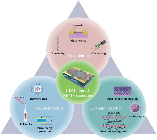
4.1 Nano-sensors
By employing LDMs-based NEMS resonators, nano-sensors achieved unprecedented sensitivities to mass, electrical charge and force. Moreover, intrinsic high elastic modulus (Table ) of LDMs enables the corresponding nano-sensors ultra-high resonant frequencies and sensitivities in assorted fields covering from physical (such as mass sensors, [Citation63,Citation158–164] ultrasound detection, [Citation125] gyroscopes, optical sensors, magnetic sensors, and thermal sensors [Citation120,Citation124,Citation165]), mechanical (force sensors, [Citation166] pressure sensors, [Citation167,Citation168] and accelerometers), chemical (gas sensors [Citation63,Citation169,Citation170]), and biological (early disease detection, [Citation171–173] DNA sequencing, [Citation160] detections of gene mutations) were reported.
4.1.1 Mass sensing
Mass sensors monitor the variations of resonance frequency when an additional mass (atomic/molecular species) is adsorbed onto the working membrane. Following equation (6), for any changes in resonance mass, the relative frequency shifts can be approximated as [Citation4,Citation89,Citation127,Citation172]
(10)
(10) where Δf0 is the resonance frequency (f0) shift and Δm is the adsorbed mass. And thus
(11)
(11) where (2meff /f0)−1 is defined as mass responsivity. In general, the lower the mass, the more sensitive the NEMS resonator reaches.
Due to the nature of low mass, small size and high stiffness, LDMs-based NEMS resonators provide sufficient mass sensitivity, for detecting individual atomic/molecular species in real time [Citation160,Citation161,Citation171]. In 2008, Jensen et al. [Citation174] achieved an atomic mass resolution and mass sensitivity of 1.3 × 10⁻²⁵ of CNTs-based resonators at room temperature. Subsequently, Lassagne et al. [Citation89] realized the mass responsivity and resolution up to be 11 Hz·yg−1 and 25 zg at room temperature (1 yg = 10−24 g and 1 zg = 10−21 g, while 1.4 zg at 5 K) in a 1-nm diameter CNTs NEMS resonator. Soon afterward, Chiu et al. [Citation114] developed an Ar atomic-scale (mAr ∼ 0.066 zg) mass sensor on the basis of the doubly-clamped CNTs resonators. In another literature, Chaste et al. [Citation127] reported a mass resolution of 1.7 yg using 150 nm-long CNTs-based resonators with the frequency close to 2 GHz, allowing detecting of the adsorption of C10H8 molecules and even the binding energy of single Xe atom adsorbed on CNTs. Moreover, the mass detecting was further realized in both the lowest-order and higher-order vibrational modes (the maximum displacement occurs at two or more positions) in single-clamped [Citation174] and doubly-clamped [Citation89,Citation162]. CNTs-based NEMS resonators. For the higher-order resonant frequency, the frequency variations depended on the motion of CNTs (especially at the adsorption point) and potentially determined both the attached mass and precise position [Citation175]. Under continuum elasticity theory, Natsuki et al. [Citation164] investigated the influence of layer number of graphene and adsorbed nanoparticles on the mass nano-sensings. The results indicated that bilayer graphene show higher mass sensitivity than monolayer graphene did. For the bilayer graphene device, the frequency shift increased with decreasing the aspect ratio and a logarithmically linear relationship between vibrational frequency and attached mass was observed for a total mass less than 10 zg.
4.1.2 Bio-sensing
Single-clamped resonators with cantilever architecture are the mainstream bio-sensors. As described by equation (11), the changes in mass or stiffness from surface biochemical effects leads to the variations in resonance frequency to complete the detection process. Following this principle, rapid and quantitative identifications of protein species were demonstrated with relatively low sample consumption. For instance, Ilic et al. [Citation160] developed SiNx-based NEMS resonator arrays and the detection of individual DNA molecule (mDNA ∼ 1.66, 1 ag = 10−18 g) was reflected by the resonant frequency shifts induced from the bound analyte. In accordance to these reports, the best mass responsivity was up to 194 Hz/ag in CNTs-based resonators. Moving forward, Naik et al. [Citation144] first developed single-biomolecule mass spectrometry based on CNTs-based resonator and achieved outstanding mass responsivity (12 Hz/zg) and sensitivity (1.66 × 10⁻² ag) for protein molecule species in real time. For certain bio- or clinical molecules in serum, urine, or saliva, the difficulties of capture or absorption process require further surface functionalization for sensing. By functionalizing trampoline surfaces toward immune-specific capture, the detection of prostate specific antigen (a protein biomarker associated with prostate cancer) was reported with clinical concentrations ranging from 50 to 50 ng/mL [Citation172].
4.1.3 Gas sensing
With the increasing attention upon human health, air-quality and its detection have been a significant and eternal topic in petroleum, food, textile and other industrial applications [Citation64,Citation176,Citation177]. According to consistent reports from several authorized institutions, environmental hazardous gases such as ammonia (NH3), nitric oxide (NO), and nitrogen dioxide (NO2) are confirmed to bring severe diseases in the respiratory tract. Therefore, it is urgent to develop reliable gas sensors to detect hazardous gases at the ppb (parts per billion) level or even lower. Gas sensors dominated by CNTs resonators operate stably at room temperature, but long recovery time and device complexity extremely limit their applications [Citation178].
Alternatively, atomic 2DMs are deemed to be ideal host materials of gas-sensors in the sub-ppb detection limit, profiting from high surface-to-volume ratio, low electronic noise, and sensitively tunable Fermi level [Citation141]. Among the 2DMs community, graphene and its derivatives are the most prevalent 2DMs for gas sensors. Based on epitaxial graphene on SiC substrate, Yu et al. [Citation170] first introduced defects into graphene and reported a NO2 sensor with a sensitivity of 105.1% for 4 ppm (part per million) with a 1 ppb detection limit. In theory, Andelic et al. [Citation169] predicted the feasibility of graphene-based NEMS resonators to detect an attached chemical warfare agent molecule. Note that the simulated results via the absolute/relative frequency-shifting method offer valuable guidance for practical graphene-based gas sensors. Stimulated by the afore-mentioned examples, Late et al. [Citation179] developed a few-layered MoS2 resonator in FET geometry and claimed that the MoS2-based gas sensor showed high responsivity to NH3, NO2, and water vapor than monolayer MoS2 counterpart at room temperature and atmospheric pressure. Later, Donarelli et al. [Citation180] investigated the gas-sensing ability of BP-based resonators at room temperature. In their experiments, BP flakes were found to be highly sensitive to NO2 and NH3 at the concentrations of 20 ppb and 10 ppm, respectively. Shi et al. [Citation141] improved the FET gas sensor by adopting few-layered BP, h-BN and MoS2 as the top-gate, dielectric layer and conducting channel, respectively. The adsorption of gas analyte by the BP gate led to the charge transfer from the gas analyte to BP. Consequently, the Fermi level and the resistance of the MoS2 channel were modulated to approach a detection limit of 3.3 ppb for NO2.
4.2. Nano-electronics
Nano-scale geometries and ultra-large surface-to-volume ratios not only offer LDMs-based NEMS resonators potential benefits in the scaling-down device and low-power consumption but also preserve efficiencies for further integration with more functional entities into one micro or nano on-chip devices [Citation4,Citation158,Citation181]. For instance, a graphene-based NEMS resonator was first implemented as the bolometer for detecting light via resonant sensing at room temperature. The principle is as follows: The absorbed light generates heat and induces thermal tensions in suspended graphene resonators, thereby shifting the corresponding resonance frequency. Employing a resonance frequency readout for photo-detection, Blaikie et al. [Citation182] achieved a room-temperature noise-equivalent power of 2 and bandwidth from 10 kHz up to 1.3 MHz. Following this trend, Verbiest et al. [Citation125] further demonstrated that graphene-based NEMS resonator could respond to the ultrasound vibration from electrical contacts up to at least 100 MHz (with a resolution of 7
). As a complementary, Lee et al. [Citation98] experimentally investigated γ-ray radiation effects in MoS2 resonators vibrating at megahertz (MHz) frequencies. They found that MoS2-based NEMS resonator exhibited excellent γ-ray radiation sensitivity (∼ 0.02–0.05 photon) and small device footprints guaranteed the integration of MoS2-based resonator on-chip, promising for compact and portable radiation detectors.
Inspirited by the biological system, the stochastic switching between two NEMS attractors facilitates the detection of weak signals of probability distributions. Intrinsic low mass and stiffness enable LDMs to get rid of large fluctuating powers to ignite stochastic switching rates of several Hz, different from conventional silicon resonators. Dolleman et al. [Citation183] demonstrated monolayer graphene resonators (drum) with stochastic switching rates up to 4.1 kHz at room temperature using optical actuation and readout. The switching rate ratio was improved by two orders of magnitude, while the effective temperature of fluctuations was reduced by three orders of magnitude in comparison with SiNx-based NEMS devices. The high-frequency stochastic switching has great advantages in transmitting weak signals in the audible frequency domain, providing opportunities for a new field for audio applications such as ultra-sensitive microphones.
Furthermore, several 2DMs exhibit piezoelectric behavior and were implemented into integral sensors, actuators and other nano-electronic applications. For instance, a piezoelectric coefficient of e11 =2.9 × 10⁻¹⁰ C/m was experimentally determined for a suspended MoS2 monolayer, [Citation184] favorable for future energy harvesting circuits and nano-sensors. In addition, the majority of LDMs withstands larger strain than Si-based ones and could be rationally patterned into curved geometries and irregular shapes. Therefore, the applications of LDMs-based NEMS sensors in low power logic circuits piezo/flexo energy generation [Citation185] and self-powered devices become feasible.
4.3. Quantum detections
In quantum physics, the quantum Hall effect, single-electron tunneling, quantum electron transport and other exotic quantum mechanical effects were reported in NEMS resonators. To bring these resonators into the quantum limit, researchers have conducted extensive research in cavity quantum photo-mechanics and cavity electro-mechanics. Passive cooling of GHz mechanical resonators through dilution refrigeration and active cooling of MHz mechanical resonators via sideband coupling to an optical or microwave cavity have successfully brought NEMS devices to the quantum mechanical ground state. In addition, due to the high-quality factors and miniscule masses, many LDMs-based NEMS resonators exhibited abnormal quantum behaviors and further advanced the understanding of quantum information processing techniques.
The couplings of excitons, spins, phonons [Citation186] and photons [Citation187] in LDMs-based NEMS resonators offer many promising avenues for condensed matter physics investigations (especially in strongly correlated electron systems), [Citation119,Citation188] sensing of force, motion and gravity beyond the standard quantum limit [Citation189] Ferromagnetism existing in many LDMs [Citation190–194] allows detecting nuclear spin with larger relaxation times, which is hopeful to be implemented into quantum memories and sensors [Citation195]. Moser et al. [Citation166] built a CNTs-based NEMS resonator and reported an unprecedented force sensitivity at the level of 12 at 1.2 K. In addition, resonant magnetic imaging with single nuclear spin resolution and magnetometry measurements of individual magnetic nanoparticle/magnet became feasible. At the monolayer limit, reduced dielectric screening and increased Coulomb interactions and may raise new exciton dynamic coupling in certain LDMs-based NEMS resonators. Besides, exciton effects and vibrations could potentially be utilized for probing charge dynamics of NEMS devices and then provide new insights into quantum states and entanglement. In this regard, Li et al. [Citation196] realized the valley-mechanical coupling in a monolayer MoS2-based NEMS resonator by exploiting the magnetic moment of valley-polarized carriers with a strong local magnetic field gradient, and demonstrated the direct transduction of valley excitation into mechanical states.
In the meantime, electron spin and the qubits (superconducting qubits, quantum dots and defect color centers) couplings were realized in mechanical NEMS resonators with high quality factors [Citation72,Citation187]. Furthermore, Kolkowitz et al. [Citation197] demonstrated that the coherent evolution of single spin with a nitrogen vacancy (NV) center in diamond could be also coupled to the mechanical vibrations of magnetized NEMS resonators constituted by an AFM tip. The coherent manipulation of the NV center spin improved the sensitivity of mechanical vibrations below 6 picometers at ambient.
5. Challenges and perspectives
With the joint efforts from materials science, chemistry, physics, nanofabrication and engineering, the adventure in LDMs-based NEMS resonators reached an unprecedented height of prosperity in the last decade, covering from fundamental mechanisms to downstream applications. Compared with current commercial resonators (KHz-MHz), the fundamental frequency of LDMs-based NEMS resonators has reached the GHz level and is expected to achieve THz level by virtue of their extremely small effective mass [Citation18]. In addition, LDMs-based NEMS devices can achieve Q values up to 10,000, surpassing the Q values (few hundred) of conventional electromechanical resonators [Citation198]. However, the NEMS appliances are heavily reliant on myriads of factors including the geometry of the working area, service environment, device configurations, fabrication procedures, and technological standards. Consequently, the vital performances fluctuate from device to device, adding immense difficulties to their commercialization. In this concern, the recognition of confronting challenges and innovative solutions to settle these issues are of particular importance to propel this revolutionary field forward. After mature evaluations, we believe that further efforts and advancements may reside in the following aspects:
Developing rational fabrication technologies and manufacturing receipts that are customized for constructing LDMs-based NEMS resonators in batch production. For each LDMs with specified structures and properties, wet-etching and drying transfer protocols are the two eternal methods to arm diverse LDMs into NEMS resonators routinely. During the transfer and following machining processes, imperfections including initial curvature, pinholes, residual strains and clusters exist in an uncontrollable and unavoidable manner, extremely limiting the device yield and repeatability. Further advances might rely on all-around developments of nanofabrication techniques and resonators architectures that congenially produce massive NEMS resonators for various LDMs with satisfying performances.
Developing simple and efficient methods for increasing Q factors. This figure of merit influences sensitivity, SNR and other design considerations but there still exists room to maximize the quality factor for LDMs-based NEMS devices. First, theoretical predictions and high-throughput screening are conducted to design or identify proper LDMs with high Q factors. Alternatively, for given LDMs, the annihilation of structural and crystal defects and optimization of architectures might be feasible to deliver elegant Q factor and even sensitivity for practical apparatus.
Prolongating the working scenes of NEMS resonators to ambient conditions. As can be seen in Table , the majority of LDMs-based NEMS resonators exhibited Q factor up to 104, force sensitivity (0.05
) and resonance frequency (1 GHz). But low temperature and vacuum conditions were indispensable, beyond the framework of modern civil devices. Therefore, encapsulations, surface/interface functionalization and other approaches that enable the steady operation of resonators under ambient conditions require more effort, no matter in a single entity or basis component for multifunctional devices.
Device integrations. The maneuverable utilizations of LDMs would help the down-scaling process with satisfying performances, have been recognized to alleviate the impact of traditional materials and out-of-date configurations. Nevertheless, further experimental and theoretical studies are advocated in this multidiscipline field and overcome the barrier to the integration of LDMs-based NEMS resonators into the Internet of Things or other electronic, photonic, and optoelectronic devices (Figure ) with better reliability and scalability at low cost.
To conclude, the aforementioned examples show the family of LDMs as one ideal material database for catering to high-performance NEMS resonators to the demands of next-generation technology. Attractive LDMs, including CNTs, graphene, h-BN, TMDCs, BP and vdW heterostructure, have been tailored to qualify NEMS resonators as ultrasensitive and cost-effectiveness sensing devices. In this review, we summarized the fabrications and critical aspects of LDMs-based NEMS resonators followed by their present and future applications. In the meantime, recent milestone works of LDMs-based NEMS resonators are also provided to keep the pace of all field-allied scientists with the latest progress in penetrating properties, actuation and detection, mechanisms and sustainably-increased quality factors toward potential device applications and integrations. We anticipated this timely and comprehensive review may offer useful insights and guidance for LDMs-based NEMS resonators, boosting intensive theoretical and experimental advances in this exciting field.
Disclosure statement
No potential conflict of interest was reported by the author(s).
Additional information
Funding
References
- Henry HXM, Zorman CA, Mehregany M, et al. Nanoelectromechanical systems: nanodevice motion at microwave frequencies. Nature. 2003;421:496.
- Hafner J, Teuschel M, Disnan D, et al. Large bias-induced piezoelectric response in the ferroelectric polymer P(VDF-TrFE) for MEMS resonators. Mater Res Lett. 2021;9:195–203.
- Craighead HG. Nanoelectromechanical systems. Science. 2000;290:1532–1535.
- Ekinci KL. Electromechanical transducers at the nanoscale: actuation and sensing of motion in nanoelectromechanical systems (NEMS). Small. 2005;1:786–797.
- Poot M, van der Zant HSJ. Mechanical systems in the quantum regime. Phys Rep. 2012;511:273–335.
- Schmid S, Villanueva LG, Roukes ML. Fundamentals of nanomechanical resonators. Cham: Springer International Publishing AG; 2016.
- Li TF, Pashkin YA, Astafiev O, et al. High-frequency metallic nanomechanical resonators. Appl Phys Lett. 2008;92:043112.
- Carr DW, Evoy S, Sekaric L, et al. Measurement of mechanical resonance and losses in nanometer scale silicon wires. Appl Phys Lett. 1999;75:920–922.
- Oh SH, Altug H, Jin X, et al. Nanophotonic biosensors harnessing van der Waals materials. Nat Commun. 2021;12:3824.
- Stankovich S, Dikin DA, Dommett GHB, et al. Graphene-based composite materials. Nature. 2006;442:282–286.
- Seo J, Swinnich E, Zhang Y, et al. Low dimensional freestanding semiconductors for flexible optoelectronics: materials, synthesis, process, and applications. Mater Res Lett. 2020;8:123–144.
- Li D, Kaner RB. Graphene-based materials. Science. 2008;320:1170–1171.
- Rogers JA, Someya T, Huang Y. Materials and mechanics for stretchable electronics. Science. 2010;327:1603–1607.
- Vogl T, Sripathy K, Sharma A, et al. Radiation tolerance of two-dimensional material-based devices for space applications. Nat Commun. 2019;10:1202.
- Iijima S. Helical microtubules of graphitic carbon. Nature. 1991;354:56–58.
- Thostenson ET, Ren Z, Chou T. Advances in the science and technology of carbon nanotubes and their composites: a review. Compos Sci Technol. 2001;61:1899–1912.
- Baughman RH, Zakhidov AA, Walt ADH. Carbon nanotubes: the route toward applications. Science. 2002;297:787–792.
- Peng HB, Chang CW, Aloni S, et al. Ultrahigh frequency nanotube resonators. Phys Rev Lett. 2006;97:87203.
- Dresselhaus MS, Jorio A, Hofmann M, et al. Perspectives on carbon nanotubes and graphene Raman spectroscopy. Nano Lett. 2010;10:751–758.
- De Volder MFL, Tawfick SH, Baughman RH, et al. Carbon nanotubes: present and future commercial applications. Science. 2013;339:535–539.
- Novoselov KS, Geim AK, Morozov SV, et al. Electric field effect in atomically thin carbon films. Science. 2004;306:666–669.
- Geim AK. Graphene: status and prospects. Science. 2009;324:1530–1534.
- Bonaccorso F, Sun Z, Hasan T, et al. Graphene photonics and optoelectronics. Nat Photonics. 2010;4:611–622.
- Gruber J, Barsoum MW, Tucker GJ. Characterization of ripplocation mobility in graphite. Mater Res Lett. 2020;8:82–87.
- Shin DH, Kim H, Lee SW. Nanoelectromechanical graphene switches for the multi-valued logic systems. Nanotechnology. 2019;30:364005.
- Xie Y, Lee J, Wang Y, et al. Straining and tuning atomic layer nanoelectromechanical resonators via comb-drive MEMS actuators. Adv Mater Technol. 2021;6:2000794.
- Ni K, Du J, Yang J, et al. Stronger interlayer interactions contribute to faster Hot carrier cooling of bilayer graphene under pressure. Phys Rev Lett. 2021;126:27402.
- Lee C, Wei X, Kysar JW, et al. Measurement of the elastic properties and intrinsic strength of monolayer graphene. Science. 2008;321:385–388.
- Saeed M, Alshammari Y, Majeed SA, et al. Chemical vapour deposition of graphene–synthesis, characterisation, and applications: A review. Molecules. 2020;25:3856.
- Wang N, Samani MK, Li H, et al. Tailoring the thermal and mechanical properties of graphene film by structural engineering. Small. 2018;14:1801346.
- Chejanovsky N, Mukherjee A, Geng J, et al. Single-spin resonance in a van der Waals embedded paramagnetic defect. Nat Mater. 2021;20:1079–1084.
- Cassabois G, Valvin P, Gil B. Hexagonal boron nitride is an indirect bandgap semiconductor. Nat Photonics. 2016;10:262–266.
- Wang QH, Kalantar-Zadeh K, Kis A, et al. Electronics and optoelectronics of two-dimensional transition metal dichalcogenides. Nat Nanotechnol. 2012;7:699–712.
- Wang Y, Nie Z, Wang F. Modulation of photocarrier relaxation dynamics in two-dimensional semiconductors. Light Sci Appl. 2020;9:192.
- Chen J, Tan J, Wu G, et al. Tunable and enhanced light emission in hybrid WS2-optical-fiber-nanowire structures. Light Sci Appl. 2019;8:8.
- Oliva R, Woźniak T, Dybala F, et al. Hidden spin-polarized bands in semiconducting 2H-MoTe2. Mater Res Lett. 2020;8:75–81.
- Mak KF, Shan J. Photonics and optoelectronics of 2D semiconductor transition metal dichalcogenides. Nat Photonics. 2016;10:216–226.
- Chitara B, Ya’akobovitz A. High-frequency electromechanical resonators based on thin GaTe. Nanotechnology. 2017;28:42LT02.
- Li L, Yu Y, Ye GJ, et al. Black phosphorus field-effect transistors. Nat Nanotechnol. 2014;9:372–377.
- Liu H, Neal AT, Zhu Z, et al. Phosphorene: an unexplored 2D semiconductor with a high hole mobility. ACS Nano. 2014;8:4033–4041.
- Youngblood N, Chen C, Koester SJ, et al. Waveguide-integrated black phosphorus photodetector with high responsivity and low dark current. Nat Photonics. 2015;9:247–252.
- Li X, Yu Z, Xiong X, et al. High-speed black phosphorus field-effect transistors approaching ballistic limit. Sci Adv. 2019;5:eaau3194.
- Kim H, Uddin SZ, Lien D, et al. Actively variable-spectrum optoelectronics with black phosphorus. Nature. 2021;596:232–237.
- Naguib M, Kurtoglu M, Presser V, et al. Two-dimensional nanocrystals produced by exfoliation of Ti3AlC2. Adv Mater. 2011;23:4248–4253.
- Shao Y, Chen C, He Q, et al. Broadband visible nonlinear absorption and ultrafast dynamics of the Ti3C2 nanosheet. Nanomaterials. 2020;10:2544.
- Castellanos-Gomez A, Singh V, van der Zant HSJ, et al. Mechanics of freely-suspended ultrathin layered materials. Ann Phys-Berlin. 2015;527:27–44.
- Novoselov KS, Mishchenko A, Carvalho A, et al. 2D materials and van der Waals heterostructures. Science. 2016;353:aac9439.
- Pei J, Yang J, Yildirim T, et al. Many-body complexes in 2D semiconductors. Adv Mater. 2019;31:1706945.
- Fan S, Vu QA, Tran MD, et al. Transfer assembly for two-dimensional van der Waals heterostructures. 2D Mater. 2020;7:22005.
- Lemme MC, Wagner S, Lee K, et al. Nanoelectromechanical sensors based on suspended 2D materials. Research. 2020;2020:8748602.
- Steeneken PG, Dolleman RJ, Davidovikj D, et al. Dynamics of 2D material membranes. 2D Mater. 2021;8:42001.
- Yildirim T, Zhang L, Neupane GP, et al. Towards future physics and applications via two-dimensional material NEMS resonators. Nanoscale. 2020;12:22366–22385.
- Barton RA, Storch IR, Adiga VP, et al. Photothermal self-oscillation and laser cooling of graphene optomechanical systems. Nano Lett. 2012;12:4681–4686.
- De Alba R, Massel F, Storch IR, et al. Tunable phonon-cavity coupling in graphene membranes. Nat Nanotechnol. 2016;11:741–746.
- Castellanos-Gomez A, Buscema M, Molenaar R, et al. Deterministic transfer of two-dimensional materials by all-dry viscoelastic stamping. 2D Mater. 2014;1:11002.
- Castellanos-Gomez A, Wojtaszek M, Tombros N, et al. Atomically thin mica flakes and their application as ultrathin insulating substrates for graphene. Small. 2011;7:2491–2497.
- Castellanos-Gomez A, van Leeuwen R, Buscema M, et al. Single-Layer MoS2 mechanical resonators. Adv Mater. 2013;25:6719–6723.
- Wang Z, Jia H, Zheng X, et al. Resolving and tuning mechanical anisotropy in black phosphorus via nanomechanical multimode resonance spectromicroscopy. Nano Lett. 2016;16:5394–5400.
- Schneider GF, Calado VE, Zandbergen H, et al. Wedging transfer of nanostructures. Nano Lett. 2010;10:1912–1916.
- Feng XL, He R, Yang P, et al. Very high frequency silicon nanowire electromechanical resonators. Nano Lett. 2007;7:1953–1959.
- Song X, Oksanen M, Sillanpää MA, et al. Stamp transferred suspended graphene mechanical resonators for radio frequency electrical readout. Nano Lett. 2012;12:198–202.
- Morell N, Reserbat-Plantey A, Tsioutsios I, et al. High quality factor mechanical resonators based on WSe2 monolayers. Nano Lett. 2016;16:5102–5108.
- Cartamil-Bueno SJ, Cavalieri M, Wang R, et al. Mechanical characterization and cleaning of CVD single-layer h-BN resonators. NPJ 2D Mater Appl. 2017;1:16.
- Arnold G, Winkler R, Stermitz M, et al. Tunable 3D nanoresonators for Gas-sensing applications. Adv Funct Mater. 2018;28:1707387.
- Teh KS. Additive direct-write microfabrication for MEMS: A review. Front. Mech Eng. 2017;12:490–509.
- Gruber G, Urgell C, Tavernarakis A, et al. Mass sensing for the advanced fabrication of nanomechanical resonators. Nano Lett. 2019;19:6987–6992.
- Sampathkumar A, Murray TW, Ekinci KL. Photothermal operation of high frequency nanoelectromechanical systems. Appl Phys Lett. 2006;88:223104.
- Verbridge SS, Parpia JM, Reichenbach RB, et al. High quality factor resonance at room temperature with nanostrings under high tensile stress. J Appl Phys. 2006;99:124304.
- van Leeuwen R, Castellanos-Gomez A, Steele GA, et al. Time-domain response of atomically thin MoS2 nanomechanical resonators. Appl Phys Lett. 2014;105:41911.
- Lee J, Wang Z, He K, et al. Electrically tunable single- and few-layer MoS2 nanoelectromechanical systems with broad dynamic range. Sci Adv. 2018;4:eaao6653.
- Barnard AW, Zhang M, Wiederhecker GS, et al. Real-time vibrations of a carbon nanotube. Nature. 2019;566:89–93.
- Wei L, Kuai X, Bao Y, et al. The recent progress of MEMS/NEMS resonators. Micromachines (Basel). 2021;12:724.
- Schmid S, Senn P, Hierold C. Electrostatically actuated nonconductive polymer microresonators in gaseous and aqueous environment. Sensor Actuat A-Phys. 2008;145-146:442–448.
- Cleland AN. Foundations of nanomechanics: from solid-state theory to device applications. New York: Springer-Verlag Berlin Heidelberg; 2003. ISBN 3-540-43661-8.
- Adiga VP, Ilic B, Barton RA, et al. Approaching intrinsic performance in ultra-thin silicon nitride drum resonators. J Appl Phys. 2012;112:64323.
- Li M, Myers EB, Tang HX, et al. Nanoelectromechanical resonator arrays for ultrafast, Gas-phase chromatographic chemical analysis. Nano Lett. 2010;10:3899–3903.
- Lee J, Wang Z, He K, et al. High frequency MoS2 nanomechanical resonators. ACS Nano. 2013;7:6086–6091.
- Yildirim T, Cho K, Wu X, et al. Probing the chaotic boundary of a membrane resonator with nanowire arrays. Nanoscale. 2017;9:17524–17532.
- Matheny MH, Villanueva LG, Karabalin RB, et al. Nonlinear mode-coupling in nanomechanical systems. Nano Lett. 2013;13:1622–1626.
- Davidovikj D, Alijani F, Cartamil-Bueno SJ, et al. Nonlinear dynamic characterization of two-dimensional materials. Nat Commun. 2017;8:1253.
- Inoue T, Anno Y, Imakita Y, et al. Resonance control of a graphene drum resonator in a nonlinear regime by a standing wave of light. ACS Omega. 2017;2:5792–5797.
- James M, Gere BJG. Mechanics of materials. Stamford: Cengage Learning; 2012. ISBN-10:1111577730.
- Villanueva LG, Karabalin RB, Matheny MH, et al. Nonlinearity in nanomechanical cantilevers. Phys Rev B. 2013;87:24304.
- Singh V, Bosman SJ, Schneider BH, et al. Optomechanical coupling between a multilayer graphene mechanical resonator and a superconducting microwave cavity. Nat Nanotechnol. 2014;9:820–824.
- Horber JKH, Miles MJ. Scanning probe evolution in biology. Science. 2003;302:1002–1005.
- Karrai K, Metzger CH. Cavity cooling of a microlever. Nature. 2004;432:1002–1005.
- Eriksson AM, Midtvedt D, Croy A, et al. Frequency tuning, nonlinearities and mode coupling in circular mechanical graphene resonators. Nanotechnology. 2013;24:395702.
- Weaver W, Timoshenko SP, Young DH. Vibration problems in engineering. New York: Wiley Inter-science; 1990.
- Lassagne B, Garcia-Sanchez D, Aguasca A, et al. Ultrasensitive mass sensing with a nanotube electromechanical resonator. Nano Lett. 2008;8:3735–3738.
- Chan J, Safavi-Naeini AH, Hill JT, et al. High-Q AlN photonic crystal nanobeam cavities fabricated by layer transfer. Appl Phys Lett. 2012;101:081115.
- Gröblacher S, Hertzberg JB, Vanner MR, et al. Demonstration of an ultracold micro-optomechanical oscillator in a cryogenic cavity. Nat Phys. 2009;5:485–488.
- Ni K-K, Norte R, Wilson DJ, et al. Enhancement of mechanical Q factors by optical trapping. Phys Rev Lett. 2012;108:214302.
- Bao M. Analysis and design principles of MEMS devices. Amsterdam: Elsevier; 2005.
- Moser J, Eichler A, Güttinger J, et al. Nanotube mechanical resonators with quality factors of up to 5 million. Nat Nanotechnol. 2014;9:1007–1011.
- Verbridge SS, Craighead HG, Parpia JM. A megahertz nanomechanical resonator with room temperature quality factor over a million. Appl Phys Lett. 2008;92:13112.
- Chen C, Lee S, Deshpande VV, et al. Graphene mechanical oscillators with tunable frequency. Nat Nanotechnol. 2013;8:923–927.
- Ye F, Lee J, Feng PXL. Electrothermally tunable graphene resonators operating at very high temperature up to 1200 K. Nano Lett. 2018;18:1678–1685.
- Lee J, Krupcale MJ, Feng PXL. Effects of γ-ray radiation on two-dimensional molybdenum disulfide (MoS2) nanomechanical resonators. Appl Phys Lett. 2016;108:23106.
- Cartamil-Bueno SJ, Steeneken PG, Tichelaar FD, et al. High-quality-factor tantalum oxide nanomechanical resonators by laser oxidation of TaSe2. Nano Res. 2015;8:2842–2849.
- Si C, Sun Z, Liu F. Strain engineering of graphene: a review. Nanoscale. 2016;8:327–3217.
- Dai H, Hafner JH, Rinzler AG, et al. Nanotubes as nanoprobes in scanning probe microscopy. Nature. 1996;384:147–150.
- Kim SH, Mulholland GW, Zachariah MR. Density measurement of size selected multiwalled carbon nanotubes by mobility-mass characterization. Carbon N Y. 2009;47:1297–1302.
- Zhang F, Hou P, Liu C, et al. Growth of semiconducting single-wall carbon nanotubes with a narrow band-gap distribution. Nat Commun. 2016;7:11160.
- Poncharal P, Wang ZL, Ugarte D, et al. Electrostatic deflections and electromechanical resonances of carbon nanotubes. Science. 1999;283:1513–1516.
- Sazonova V, Yaish Y, Ustunel H, et al. A tunable carbon nanotube electromechanical oscillator. Nature. 2004;431:284–287.
- Benjamin L, Yury T, Jari K, et al. Coupling mechanics to charge transport in carbon nanotube mechanical resonators. Science. 2009;325:1107–1110.
- Bai Y, Yue H, Wang J, et al. Super-durable ultralong carbon nanotubes. Science. 2020;369:1104–1106.
- Garcia-Sanchez D, San Paulo A, Esplandiu MJ, et al. Mechanical detection of carbon nanotube resonator vibrations. Phys Rev Lett. 2007;99:85501.
- de Bonis SL, Urgell C, Yang W, et al. Ultrasensitive displacement noise measurement of carbon nanotube mechanical resonators. Nano Lett. 2018;18:5324–5328.
- Levi R, Garel J, Teich D, et al. Nanotube electromechanics beyond carbon: The case of WS2. ACS Nano. 2015;9:12224–12232.
- Kumar M, Bhaskaran H. Ultrasensitive room-temperature piezoresistive transduction in graphene-based nanoelectromechanical systems. Nano Lett. 2015;15:2562–2567.
- Ning ZY, Shi TW, Fu MQ, et al. Transversally and axially tunable carbon nanotube resonators In situ fabricated and studied inside a scanning electron microscope. Nano Lett. 2014;14:1221–1227.
- Laird EA, Pei F, Tang W, et al. A high quality factor carbon nanotube mechanical resonator at 39 GHz. Nano Lett. 2012;12:193–197.
- Steele GA, Hüttel AK, Witkamp B, et al. Strong coupling between single-electron tunneling and nanomechanical motion. Science. 2009;325:1103–1107.
- Barton RA, Ilic B, van der Zande AM, et al. High, size-dependent quality factor in an array of graphene mechanical resonators. Nano Lett. 2011;11:1232–1236.
- Eichler A, Moser J, Chaste J, et al. Nonlinear damping in mechanical resonators made from carbon nanotubes and graphene. Nat Nanotechnol. 2011;6:339–342.
- Naik A, Buu O, LaHaye MD, et al. Cooling a nanomechanical resonator with quantum back-action. Nature. 2006;443:193–196.
- Urgell C, Yang W, De Bonis SL, et al. Cooling and self-oscillation in a nanotube electromechanical resonator. Nat Phys. 2019;16:32–37.
- Deng G, Zhu D, Wang X, et al. Strongly coupled nanotube electromechanical resonators. Nano Lett. 2016;16:5456–5462.
- Chen C, Rosenblatt S, Bolotin KI, et al. Performance of monolayer graphene nanomechanical resonators with electrical readout. Nat Nanotechnol. 2009;4:861–867.
- Bunch JS, van der Zande AM, Verbridge SS, et al. Electromechanical resonators from graphene sheets. Science. 2007;315:490–493.
- Zhang X, Makles K, Colombier L, et al. Dynamically-enhanced strain in atomically thin resonators. Nat Commun. 2020;11:5526.
- Keşkekler A, Shoshani O, Lee M, et al. Tuning nonlinear damping in graphene nanoresonators by parametric–direct internal resonance. Nat Commun. 2021;12:1099.
- Singh V, Sengupta S, Solanki HS, et al. Probing thermal expansion of graphene and modal dispersion at low-temperature using graphene nanoelectromechanical systems resonators. Nanotechnology. 2010;21:165204.
- Verbiest GJ, Kirchhof JN, Sonntag J, et al. Detecting ultrasound vibrations with graphene resonators. Nano Lett. 2018;18:5132–5137.
- Davidovikj D, Poot M, Cartamil-Bueno SJ, et al. On-chip heaters for tension tuning of graphene nanodrums. Nano Lett. 2018;18:2852–2858.
- Chaste J, Eichler A, Moser J, et al. A nanomechanical mass sensor with yoctogram resolution. Nat Nanotechnol. 2012;7:301–304.
- Jung M, Rickhaus P, Zihlmann S, et al. GHz nanomechanical resonator in an ultraclean suspended graphene p-n junction. Nanoscale. 2019;11:4355–4361.
- Robinson JT, Zalalutdinov M, Baldwin JW, et al. Wafer-scale reduced graphene oxide films for nanomechanical devices. Nano Lett. 2008;8:3441–3445.
- Zalalutdinov MK, Robinson JT, Junkermeier CE, et al. Engineering graphene mechanical systems. Nano Lett. 2012;12:4212–4218.
- Su Z, Ying Y, Song X, et al. Tunable parametric amplification of a graphene nanomechanical resonator in the nonlinear regime. Nanotechnology. 2021;32:155203.
- Singh R, Sarkar A, Guria C, et al. Giant tunable mechanical nonlinearity in graphene–silicon nitride hybrid resonator. Nano Lett. 2020;20:4659–4666.
- Verbiest GJ, Goldsche M, Sonntag J, et al. Tunable coupling of two mechanical resonators by a graphene membrane. 2D Mater. 2021;8:035039.
- Miller D, Blaikie A, Alemán BJ. Nonvolatile rewritable frequency tuning of a nanoelectromechanical resonator using photoinduced doping. Nano Lett. 2020;20:2378–2386.
- Lee J, Wang Z, He K, et al. Air damping of atomically thin MoS2 nanomechanical resonators. Appl Phys Lett. 2014;105:23104.
- Chitara B, Ya'Akobovitz A. Tunable wide-bandwidth resonators based on layered gallium sulfide. Part Part Syst Char. 2019;36:1800460.
- Wang Z, Yang R, Feng PXL. Thermal hysteresis controlled reconfigurable MoS2 nanomechanical resonators. Nanoscale. 2021;13:18089–18095.
- Xie H, Jiang S, Rhodes DA, et al. Tunable exciton-optomechanical coupling in suspended monolayer MoSe2. Nano Lett. 2021;21:2538–2543.
- Wang X, Lan S. Optical properties of black phosphorus. Adv Opt Photonics. 2016;8:618.
- Wei Q, Peng X. Superior mechanical flexibility of phosphorene and few-layer black phosphorus. Appl Phys Lett. 2014;104:251915.
- Shi S, Hu R, Wu E, et al. Highly-sensitive gas sensor based on two-dimensional material field effect transistor. Nanotechnology. 2018;29:435502.
- Wang Z, Jia H, Zheng X, et al. Black phosphorus nanoelectromechanical resonators vibrating at very high frequencies. Nanoscale. 2015;7:877–884.
- Castellanos-Gomez A, Wojtaszek M, Tombros N, et al. Atomically thin mica flakes and their application as ultrathin insulating substrates for graphene. Small. 2011;7:465–468.
- Wang Z, Lee J, Feng PXL. Spatial mapping of multimode Brownian motions in high-frequency silicon carbide microdisk resonators. Nat Commun. 2014;5:515.
- Zheng X, Lee J, Feng PXL. Hexagonal boron nitride nanomechanical resonators with spatially visualized motion. Microsyst Nanoeng. 2017;3:17038.
- Wang Y, Lee J, Zheng X, et al. Hexagonal boron nitride phononic crystal waveguides. ACS Photonics. 2019;6:3225–3232.
- Wang L, Meric I, Huang PY, et al. One-dimensional electrical contact to a two-dimensional material. Science. 2013;342:614–617.
- Dean CR, Young AF, Meric I, et al. Boron nitride substrates for high-quality graphene electronics. Nat Nanotechnol. 2010;5:722–726.
- Lee CH, Lee GH, van der Zande AM, et al. Atomically thin p-n junctions with van der waals heterointerfaces. Nat Nanotechnol. 2014;9:676–681.
- Will M, Hamer M, Müller M, et al. High quality factor graphene-based Two-dimensional heterostructure mechanical resonator. Nano Lett. 2017;17:5950–5955.
- Güttinger J, Noury A, Weber P, et al. Energy-dependent path of dissipation in nanomechanical resonators. Nat Nanotechnol. 2017;12:631–636.
- Dienwiebel M, Verhoeven GS, Pradeep N, et al. Superlubricity of graphite. Phys Rev Lett. 2004;92:126101.
- Leven I, Krepel D, Shemesh O, et al. Robust superlubricity in graphene/h-BN heterojunctions. J Phys Chem Lett. 2013;4:115–120.
- Alden JS, Tsen AW, Huang PY, et al. Strain solitons and topological defects in bilayer graphene. Proc Natl Acad Sci USA. 2013;110:11256–11260.
- Benameur MM, Gargiulo F, Manzeli S, et al. Electromechanical oscillations in bilayer graphene. Nat Commun. 2015;6:8582.
- Ye F, Lee J, Feng PXL. Atomic layer MoS2-graphene van der Waals heterostructure nanomechanical resonators. Nanoscale. 2017;9:18208–18215.
- Kim S, Yu J, van der Zande AM. Nano-electromechanical drumhead resonators from two-dimensional material bimorphs. Nano Lett. 2018;18:6686–6695.
- Arash B, Jiang J, Rabczuk T. A review on nanomechanical resonators and their applications in sensors and molecular transportation. appl. Phys Rev. 2015;2:21301.
- Zhang Z, Wu Y, Sang L, et al. Coupling of magneto-strictive FeGa film with single-crystal diamond MEMS resonator for high-reliability magnetic sensing at high temperatures. Mater Res Lett. 2020;8:180–186.
- Ilic B, Yang Y, Aubin K, et al. Enumeration of DNA molecules bound to a nanomechanical oscillator. Nano Lett. 2005;5:925–929.
- Eom K, Yang J, Park J, et al. Experimental and computational characterization of biological liquid crystals: A review of single-molecule bioassays. Int J Mol Sci. 2009;10:4009–4032.
- Chiu H, Hung P, Postma HWC, et al. Atomic-Scale mass sensing using carbon nanotube resonators. Nano Lett. 2008;8:4342–4346.
- Lee H, Yang Y, Chang W. Mass detection using a graphene-based nanomechanical resonator. Jpn J Appl Phys. 2013;52:25101.
- Natsuki T, Shi J, Ni Q. Vibration analysis of nanomechanical mass sensor using double-layered graphene sheets resonators. J Appl Phys. 2013;114:094307.
- Roy SK, Sauer VTK, Westwood-Bachman JN, et al. Improving mechanical sensor performance through larger damping. Science. 2018;360:eaar5220.
- Moser J, Guttinger J, Eichler A, et al. Ultrasensitive force detection with a nanotube mechanical resonator. Nat Nanotechnol. 2013;8:493–496.
- Jiang S, Gong X, Guo X, et al. Potential application of graphene nanomechanical resonator as pressure sensor. Solid State Commun. 2014;193:30–33.
- Song P, Si C, Zhang M, et al. A novel piezoresistive MEMS pressure sensors based on temporary bonding technology. Sensors. 2020;20:337.
- Anđelić N, Car Z, Čanađija M. NEMS resonators for detection of chemical warfare agents based on graphene sheet. Math Probl Eng. 2019;2019:1–23.
- Yu C, Liu Q, He Z, et al. Epitaxial graphene gas sensors on SiC substrate with high sensitivity. J Semicond. 2020;41:032101.
- Naik AK, Hanay MS, Hiebert WK, et al. Towards single-molecule nanomechanical mass spectrometry. Nat Nanotechnol. 2009;4:445–450.
- Waggoner PS, Varshney M, Craighead HG. Detection of prostate specific antigen with nanomechanical resonators. Lab Chip. 2009;9:3095.
- Johnson BN, Mutharasan R. Biosensing using dynamic-mode cantilever sensors: A review. Biosens Bioelectron. 2012;32:1–18.
- Jensen K, Kim K, Zettl A. An atomic-resolution nanomechanical mass sensor. Nat Nanotechnol. 2008;3:533–537.
- Knobel RG. Weighing single atoms with a nanotube. Nat Nanotechnol. 2008;3:525–526.
- Wu Y, Joshi N, Zhao S, et al. NO2 gas sensors based on CVD tungsten diselenide monolayer. Appl Surf Sci. 2020;529:147110.
- Joshi N, Braunger ML, Shimizu FM, et al. In: Kumar Tuteja S, Arora D, Dilbaghi N, Lichtfouse E, editor. Nanosensors for environmental applications. Cham: Springer International Publishing; 2020.
- Wang Y, Yeow JTW. A review of carbon nanotubes-based gas sensors. J Sens. 2009;2009:1–24.
- Late DJ, Huang Y, Liu B, et al. Sensing behavior of atomically thin-layered MoS2 transistors. ACS Nano. 2013;7:4879–4891.
- Donarelli M, Ottaviano L, Giancaterini L, et al. Exfoliated black phosphorus gas sensing properties at room temperature. 2D Mater. 2016;3:25002.
- Blaikie A, Miller D, Alemán BJ. A fast and sensitive room-temperature graphene nanomechanical bolometer. Nat Commun. 2019;10:4726.
- Xu Y, Chen C, Deshpande VV, et al. Radio frequency electrical transduction of graphene mechanical resonators. Appl Phys Lett. 2010;97:243111.
- Dolleman RJ, Belardinelli P, Houri S, et al. High-Frequency stochastic switching of graphene resonators near room temperature. Nano Lett. 2019;19:1282–1288.
- Zhu H, Wang Y, Xiao J, et al. Observation of piezoelectricity in free-standing monolayer MoS2. Nat Nanotechnol. 2015;10:151–155.
- Wu W, Wang L, Li Y, et al. Piezoelectricity of single-atomic-layer MoS2 for energy conversion and piezotronics. Nature. 2014;514:470–474.
- Oeckinghaus T, Momenzadeh SA, Scheiger P, et al. Spin-phonon interfaces in coupled nanomechanical cantilevers. Nano Lett. 2020;20:463–469.
- Aspelmeyer M, Kippenberg TJ, Marquardt F. Cavity optomechanics. Rev Mod Phys. 2014;86:1391–1452.
- Benyamini A, Hamo A, Kusminskiy SV, et al. Real-space tailoring of the electron-phonon coupling in ultraclean nanotube mechanical resonators. Nat Phys. 2014;10:151–156.
- Møller CB, Thomas RA, Vasilakis G, et al. Quantum back-action-evading measurement of motion in a negative mass reference frame. Nature. 2017;547:191–195.
- Gong C, Li L, Li Z, et al. Discovery of intrinsic ferromagnetism in two-dimensional van der Waals crystals. Nature. 2017;546:265–269.
- Huang B, Clark G, Navarro-Moratalla E, et al. Layer-dependent ferromagnetism in a van der Waals crystal down to the monolayer limit. Nature. 2017;546:270–273.
- Bonilla M, Kolekar S, Ma Y, et al. Strong room-temperature ferromagnetism in VSe2 monolayers on van der Waals substrates. Nat Nanotechnol. 2018;13:289–293.
- Zhang Z, Shang J, Jiang C, et al. Direct photoluminescence probing of ferromagnetism in monolayer two-dimensional CrBr3. Nano Lett. 2019;19:3138–3142.
- Bozhko DA, Vasyuchka VI, Chumak AV, et al. Magnon-phonon interactions in magnon spintronics. Low Temp Phys. 2020;46:383–399.
- Okazaki Y, Mahboob I, Onomitsu K, et al. Dynamical coupling between a nuclear spin ensemble and electromechanical phonons. Nat Commun. 2018;9:2993.
- Li H, Fong KY, Zhu H, et al. Valley optomechanics in a monolayer semiconductor. Nat Photonics. 2019;13:397–401.
- Kolkowitz S, Jayich AC, Unterreithmeier QP, et al. Coherent sensing of a mechanical resonator with a single-spin qubit. Science. 2012;335:1603–1606.
- Andreani P, Bevilacqua A. Harmonic oscillators in CMOS—A tutorial overview. IEEE Open J Solid-State Circuits Soc. 2021;1:2–17.
- Van der Zande AM, Barton RA, Alden JS, et al. Large-scale arrays of single-layer graphene resonators. Nano Lett. 2010;10:4869–4873 .
- Jia H, Yang R, Nguyen AE, et al. Large-scale arrays of single- and few-layer MoS2 nanomechanical resonators. Nanoscale. 2016;8:10677–10685.
- Feng XL, White CJ, Hajimiri A, et al. A self-sustaining ultrahigh-frequency nanoelectromechanical oscillator. Nat Nanotechnol. 2008;3:342–346.
- Villanueva LG, Karabalin RB, Matheny MH, et al. A nanoscale parametric feedback oscillator. Nano Lett. 2011;11:5054–5059.
- Cleland AN, Roukes ML. Fabrication of high frequency nanometer scale mechanical resonators from bulk Si crystals. Appl Phys Lett. 1996;69:2653–2655.
- Sartori AF, Belardinelli P, Dolleman RJ, et al. Inkjet-printed high-Q nanocrystalline diamond resonators. Small. 2019;15:1803774.
- Arcizet O, Jacques V, Siria A, et al. A single nitrogen-vacancy defect coupled to a nanomechanical oscillator. Nat Phys. 2011;7:879–883.
- Zhang ZZ, Hu Q, Song XX, et al. A suspended silicon single-hole transistor as an extremely scaled gigahertz nanoelectromechanical beam resonator. Adv Mater. 2020;32:2005625.
- Yao N, Lordi V. Young’s modulus of single-walled carbon nanotubes. J Appl Phys. 1998;84:1939–1943.
- Yakobson BI, Brabec CJ, Berhnolc J. Nanomechanics of carbon tubes: instabilities beyond linear response. Phys Rev Lett. 1996;76:2511–2514.
- King A, Johnson G, Engelberg D, et al. Observations of intergranular stress corrosion cracking in a grain-mapped polycrystal. Science. 2008;321:382–385.
- Liu F, Ming P, Li J.; Ab initio calculation of ideal strength and phonon instability of graphene under tension. Phys Rev B. 2007;76:064120.
- Zhao J, Deng Q, Ly TH, et al. Two-dimensional membrane as elastic shell with proof on the folds revealed by three-dimensional atomic mapping. Nat Commun. 2015;6:8935.
- Schwierz F. Graphene transistors. Nat Nanotechnol. 2010;5:487–496.
- Song L, Ci L, Lu H, et al. Large scale growth and characterization of atomic hexagonal boron nitride layers. Nano Lett. 2010;10:3209–3215.
- Kudin KN, Scuseria GE, Yakobson BI. C2f, BN, and C nanoshell elasticity from ab initio computations. Phys Rev B. 2001;64:235406.
- Bertolazzi S, Brivio J, Kis A. Stretching and breaking of ultrathin MoS2. ACS Nano. 2011;5:9703–9709.
- Feldman JL. Elastic constants of 2H-MoS2 and 2H-NbSe2 extracted from measured dispersion curves and linear compressibilities. J Phys Chem Solids. 1976;37:1141–1144.
- Samanta C, Yasasvi Gangavarapu PR, Naik AK. Nonlinear mode coupling and internal resonances in MoS2 nanoelectromechanical system. Appl Phys Lett. 2015;107:173110.
- Kappera R, Voiry D, Yalcin SE, et al. Phase-engineered low-resistance contacts for ultrathin MoS2 transistors. Nat Mater. 2014;13:1128–1134.
- Liu K, Yan Q, Chen M, et al. Elastic properties of chemical-vapor-deposited monolayer MoS2, WS2, and their bilayer heterostructures. Nano Lett. 2014;14:5097–5103.
- Zhang X, Dong Q, Li Z, et al. Significant pressure-induced enhancement of photoelectric properties of WS2 in the near-infrared region. Mater Res Lett. 2022;10:547–555.
- Alharbi A, Shahrjerdi D. Electronic properties of monolayer tungsten disulfide grown by chemical vapor deposition. Appl Phys Lett. 2016;109:193502.
- Çakır D, Peeters FM, Sevik C. Mechanical and thermal properties of h-MX2 (M = Cr, Mo, W; X = O, S, Se, Te) monolayers: A comparative study. Appl Phys Lett. 2014;104:203110.
- Bhattacharyya R, Misra A, Sandeep KC. Photovoltaic solar energy conversion for hydrogen production by alkaline water electrolysis: conceptual design and analysis. Energ Convers Manage. 2017;133:1–3.
- Jones AM, Yu H, Ghimire NJ, et al. Optical generation of excitonic valley coherence in monolayer WSe2. Nat Nanotechnol. 2013;8:634–638.
- Ovchinnikov D, Allain A, Huang YS, et al. Electrical transport properties of single-layer WS2. ACS Nano. 2014;8:8174–8181.
- Zeng F, Zhang W, Tang B. Electronic structures and elastic properties of monolayer and bilayer transition metal dichalcogenides MX2 (M = Mo, W; X = O, S, Se, Te): A comparative first-principles study. Chin Phys B. 2015;24:97103.
- Lai K, Zhang W, Zhou F, et al. Bending rigidity of transition metal dichalcogenide monolayers from first-principles. J Phy D: Appl Phys. 2016;49:185301.
- Wilson JA, Yoffe A. The transition metal dichalcogenides discussion and interpretation of the observed optical, electrical and structural properties. Adv Phys. 1969;18:193–335.
- Zhang W, Huang Z, Zhang W, et al. Two-dimensional semiconductors with possible high room temperature mobility. Nano Res. 2014;7:1731–1737.
- Keum DH, Cho S, Kim JH, et al. Bandgap opening in few-layered monoclinic MoTe2. Nat Phys. 2015;11:482–486.
- Chitara B, Ya'Akobovitz A. Elastic properties and breaking strengths of GaS, GaSe and GaTe nanosheets. Nanoscale. 2018;10:13022–13027.
- Hu P, Wang L, Yoon M, et al. Highly responsive ultrathin GaS nanosheet photodetectors on rigid and flexible substrates. Nano Lett. 2013;13:1649–1654.
- Jiang J, Park HS. Mechanical properties of single-layer black phosphorus. J Phy D: Appl Phys. 2014;47:385304.
- Zhang HY, Jiang JW. Elastic bending modulus for single-layer black phosphorus. J Phys D: Appl Phys. 2015;48:455305.
- Qiao J, Kong X, Hu ZX, et al. High-mobility transport anisotropy and linear dichroism in few-layer black phosphorus. Nat Commun. 2014;5:4475.