
ABSTRACT
Niobium superconducting radiofrequency cavities enable applications in modern accelerators and quantum computers. However, the surface resistance significantly deteriorates the cavities’ performance. Nitrogen doping surface treatment can consistently increase cavity performance by reducing surface resistance, but the improvement mechanism is not fully understood. Herein, we employed transmission electron microscopy and spectroscopy to uncover the structural and chemical differences of the Nb/air interface between the non-doped and nitrogen-doped cavities. The results indicate that nitrogen doping passivates the Nb surface by introducing a compressive stress/strain close to the Nb/air interface, which impedes the diffusion of oxygen and hydrogen atoms and reduces surface oxide thickness.
GRAPHICAL ABSTRACT

IMPACT STATEMENT
A comprehensive structural and chemical study of the Nb/air interface from the non-doped and nitrogen-doped niobium cavity helps to understand the performance improvement mechanisms of the nitrogen-doped cavity.
Introduction
Niobium superconducting radiofrequency (SRF) cavities are an essential component for particle accelerators [Citation1] and quantum computers [Citation2]. The performance of the SRF cavity is determined by its quality factor (Q-factor) [Citation3], which is inversely proportional to the surface resistance (Rs). Extensive research has been done on the microwave surface resistance of Nb cavities, identifying its critical contribution to radiofrequency (RF) losses at varying frequencies, including the deteriorating Q-factor (Q-drop) with increasing accelerating fields [Citation1,Citation4]. The Rs of the Nb cavities mainly originates in a thin surface layer given by the superconducting Nb penetration depth ∼45 nm, with crucial contributions from the Nb/air interface. The complex amorphous oxidation layer [Citation5] and Nb hydrides precipitation on Nb surfaces [Citation6,Citation7] lead to non-superconducting regions that cause serious degradation.
It is of interest to identify all sources of RF losses and to mitigate such problems to improve performance of superconducting RF cavities and qubits. The formation of an amorphous oxidation layer, with a saturated thickness of ∼ 6 nm, is unavoidable in the ambient atmosphere without any passivation [Citation8]. The oxidation layer comprises multi-layer (sub-)oxides [Citation3,Citation9,Citation10], where the Nb2O5 phase is dominant (over ∼ 70% of the total thickness) [Citation11]. The suboxides include metallic NbO and semiconducting NbO2, each of which is thermodynamically stable with off-stoichiometry. The mixture of the various oxides at the top surface can increase the surface resistance of the Nb SRF cavity in several ways [Citation12]. NbO is metallic with a superconducting critical temperature TC ∼1.38 K, considerably lower than Nb [Citation13], causing a higher Bardeen–Cooper–Schrieffer (BCS) surface resistance. Vacancies in Nb2O5 are magnetic [Citation14] and lead to conducting behavior at ∼3% concentration, possibly giving rise to nonequilibrium quasiparticle non-two-level-system (TLS) losses [Citation15]. Studies of SRF cavities for 3D qubits reveal evidence of TLS loss and an order of magnitude increase in Q-factor of cavity with the removal of the oxide layer via vacuum annealing [Citation16]. These results indicate that the Nb oxides layer could be a source of both TLS and non-TLS RF losses. Meanwhile, the hydrogen absorption of Nb is usually inevitable since the cavity is processed via multiple polishing procedures during its fabrication [Citation17]. Once hydrogen atoms diffuse into Nb metal, hydride precipitations form near the surface when the metal is cooled below ∼170 K [Citation6,Citation18]. These hydrides, with superconducting temperature <1.3 K [Citation7], dramatically decrease the Q-factor of the cavity [Citation19].
Different treatments, such as low-temperature baking [Citation20] and advanced surface polishing strategies [Citation21], have effectively decreased the surface resistance while increasing the Q-factor of SRF cavities in the past few decades. For example, Ciovati [Citation20] baked the cavities between 100 - 200 °C under an ultrahigh vacuum, reducing the Q-drop at high magnetic fields. Copper et al. [Citation22] combined mechanical polishing with light electropolishing on the cavity, which decreased the surface roughness and enhanced the Q-factor to ∼3×10¹⁰. The rationale is to reduce surface resistance by eliminating the surface oxidation layer. However, a substantial increase in surface resistance has still been observed in varying magnetic fields [Citation20,Citation23], due to the (sub-)oxides and hydrides formed after baking or polishing. Therefore, a method that simultaneously limits the RF losses of the oxidation layer and hydride formation is necessary to further reduce surface resistance.
Nitrogen doping (N-doping) or infusion (N-infusion) has become a predominant method of reducing surface resistance [Citation24,Citation25]. The low-temperature N-infusion, identified by Grassellino et al. [Citation26], exposes the SRF cavities to ∼25 mTorr N2 for 48 h at 120 °C, significantly increasing the Q-factor to over ∼5×10¹⁰, almost twice as the non-infused sample. The surface resistance can be maintained at a minimal value over a range of magnetic fields (0 mT to 80 mT) in N-doped cavities [Citation27]. In addition, significant improvements in the Q-factor of SRF cavities after N-doping/infusion have been observed over a broad range of frequencies (0.65 GHz to 3.9 GHz) [Citation26,Citation28,Citation29]. Thus, the N-doping or N-infusion method has greatly increased the performance of SRF cavities in various applications. However, the mechanism which controls N-doping into Nb cavities and their thermodynamic stability are uncertain. Theoretical simulations [Citation30,Citation31] claim that interstitial N atoms can suppress Nb hydrides’ formation and stability, thus improving Q-factor. But there is a lack of experimental validation of the structural and chemical change of the (sub-)surface caused by N-doping/infusion at the atomic scale, the diffusive pathways, and the stability of the N in the near-surface. The unclear mechanistic understanding impedes further development of surface treatment to improve the Q-factor of SRF cavities.
This paper presents a comprehensive structural and chemical investigation of the complex Nb/air interface of the non-doped and N-doped Nb SRF cavities. 100 and 110 Nb facets are observed at the Nb/NbOx interface for both samples. Nitrogen atoms may diffuse into the octahedral interstitial site of the Nb lattice during doping treatment through these facets [Citation32], causing high compressive stress/strain near the Nb surface. The N interstitials and compressive stress/strain impede the diffusion of oxygen and hydrogen atoms, consequently suppressing the oxidation and formation of hydrides. As a result, the oxidation layer thickness of the N-doped sample is ∼20% thinner than that of the non-doped sample. The strain relaxation also tends to induce crystallization in the newly formed amorphous NbOx layer. These results clarify the mechanism of the surface resistance reduction by N-doping in the SRF cavity.
Materials and methods
Two groups of Nb cavities, N-doped and non-doped samples, were received from Fermi Lab. The detailed fabrication process of N-doped cavity has been reported in Ref [Citation25, Citation26]. For local misorientation mapping by electron backscattered diffraction (EBSD), scan was performed under 20 kV and 16 nA electron beam at step size 0.5 µm, with a binning size of 8 × 8. A focused ion beam (FIB, FEI Helios NanoLab G3) was used to prepare the TEM samples with the lift-out technique. A permanent maker was applied as a protective layer before carbon deposition. The microstructure of all the samples was examined using a probe aberration-corrected Titan Themis TEM equipped with a Super-X EDS detector and a quantum 965 GIF system.
Results and discussion
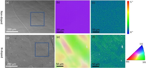
The N-doped and non-doped cavities show a clear surface strain difference. Optical microscopy images confirm the grain size of the non-doped sample is ∼300 µm to 800 µm, while the grain size of the N-doped sample is ∼50 µm to 400 µm (Figure a and c). Interestingly, the backscattered SEM images in Figure b and d show the contrast is uniform within each grain of the non-doped sample, while the contrast varies in the grains of the N-doped sample. This irregular contrast suggests the existence of grain misorientation or a change in the degree of deformation near the surface in the N-doped cavities [Citation33]. To quantitatively analyze the local misorientation, the EBSD result is obtained from a ∼250 µm × 250 µm region within one grain both from non-doped and N-doped samples, as shown in Figure a and d. The inverse pole figure (IPF) coloring map shows only one color for the region in the non-doped sample (Figure b). In contrast, several domains with different colors are discovered in the N-doped sample (Figure e), indicating the formation of subgrains or low-angle boundaries. The kernel average misorientation (KAM) mapping in Figure c and f, representing the local misorientation, is often used for strain analysis [Citation34]. The local misorientation of the N-doped sample is significantly higher than that of the non-doped sample, indicating the higher strain level at the surface by N-doping [Citation34], which is consistent with the SEM results. The N-doped sample’s high surface strain is likely due to the diffusion of N atoms into the Nb lattice during surface treatment [Citation22], similar to the hardening process for carburized steel with high in-plane compressive stress/strain near the surface [Citation35,Citation36].
Figure 1. Surface morphology characterization. The optical (a, c) and back scattered SEM (b, d) images of the non-doped (a-b) and nitrogen-doped (c-d) samples.
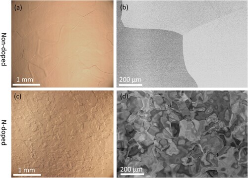
Figure 2. EBSD analysis of local misorientation. (a-c) non-doped sample and (d-f) N-doped sample. The blue squares in (a) and (d) indicate the ∼ 250 µm × 250 µm region within a coarse grain for EBSD scanning; IPF map of (b) non-doped and (e) N-doped samples, the domains with different colors in (e) represent regions with different orientations; (c) and (f) the corresponding KAM mapping of (b) and (e).
A relatively uniform ∼ 6 nm amorphous NbOx layer is revealed in the non-doped sample (Figure a). Corresponding energy-dispersive X-ray spectroscopy (EDS) elemental mappings (Figure S1a-d) display uniform O and Nb distribution inside the NbOx layer. The Nb metal shows 110 or 100 facets at the Nb/NbOx interface by atomic resolution bright-field (BF) STEM image, as indicated in Figure b. These facets are formed in the close-packed planes in Nb to minimize interface energy [Citation37]. Both facets have a 2∼4 monolayers step at the interface and the steps generate a 4∼6 monolayers terrace. The morphology of the facets (steps and terraces) tends to have different superconducting gaps, thus impacting the cavities’ performance [Citation33]. Meanwhile, the 110 and 100 facets provide a larger interface area for the diffusion [Citation38,Citation39]. Since O or H atoms prefer to diffuse into the interstitial sites of the Nb lattice (schematic in Figure c) [Citation30,Citation40,Citation41], the facets at the Nb/NbOx interface could facilitate subsequent formation of Nb (sub-)oxides or hydrides.
Figure 3. Microstructural and chemical analysis at Nb surface of the non-doped sample. (a) HRTEM image taken along [001] zone axis (ZA). (b) High-resolution BF-STEM image (top right inset is the corresponding fast Fourier transformation (FFT) image) shows the NbOx/Nb interface area. The white and red arrows indicate the 100 and 110 facets. The inset at the bottom right shows Nb lattice distortion close to the NbOx/Nb interface (indicated by light blue arrow). (c) schematic of Nb crystal structure with interstitial oxygen at the octahedral center, viewed along [001] ZA; (d) ABF image near the NbOx/Nb interface. The oxygen interstitials are indicated by blue arrows. (e-g) EELS analysis of the NbOx layer: (e) HAADF-STEM image and the first derivative of EELS line scan (color inset) of the Nb-M3 and O-K edges; (f-g) EELS spectrum of Nb-M2, 3 and O-K edges from positions 1–4 in (e).
![Figure 3. Microstructural and chemical analysis at Nb surface of the non-doped sample. (a) HRTEM image taken along [001] zone axis (ZA). (b) High-resolution BF-STEM image (top right inset is the corresponding fast Fourier transformation (FFT) image) shows the NbOx/Nb interface area. The white and red arrows indicate the 100 and 110 facets. The inset at the bottom right shows Nb lattice distortion close to the NbOx/Nb interface (indicated by light blue arrow). (c) schematic of Nb crystal structure with interstitial oxygen at the octahedral center, viewed along [001] ZA; (d) ABF image near the NbOx/Nb interface. The oxygen interstitials are indicated by blue arrows. (e-g) EELS analysis of the NbOx layer: (e) HAADF-STEM image and the first derivative of EELS line scan (color inset) of the Nb-M3 and O-K edges; (f-g) EELS spectrum of Nb-M2, 3 and O-K edges from positions 1–4 in (e).](/cms/asset/e8d1cca5-2891-46f2-80a2-aa55bce5d6e7/tmrl_a_2126737_f0003_oc.jpg)
Some interstitial oxygen atoms are visible by angular bright-field (ABF) imaging, which is an imaging mode that is sensitive to light elements by using an annular detector with a collection angle of 11 mrad-22 mrad [Citation42]. Figure d shows an atomic resolution ABF image around the NbOx/Nb interface. The O atomic positions are labeled by blue arrows, consistent with the schematic in Figure c. The interstitial O atoms are stable and may not be released below 1600 °C [Citation10]. Moreover, these interstitial O atoms distort the Nb lattice and introduce strain at the interface, as demonstrated by the lattice image in Figure d.
There is a transition of the valence state of Nb in the NbOx layer across the NbOx/Nb interface, as shown by the electron energy loss spectra (EELS) in Figure e–g. The Nb-M2,3 and O-K edge can distinguish different oxides (NbO, NbO2, or Nb2O5) [Citation12]. The Nb M2 and M3 edge is mainly attributed to the transition of Nb 3p electrons to unoccupied Nb 4d and 5s states, where the spin–orbit coupling of the 3p electrons results in the two sharp edges, namely the M3 and M2 [Citation12]. With the valence changes from Nb (0) to Nb (+5), a right shift of the M3 or M2 edges will be observed. An EELS line scan across the NbOx (step size ∼ 0.3 nm) and the color map generated by the first derivative method of the spectrum [Citation43] are shown in Figure e. There is an apparent shift of Nb-M3 and O-K edge position across the Nb/NbOx interface. After moving ∼1.5 nm from the interface into the NbOx layer, the Nb-M3 and O-K edges shift again. These shifts imply the valance changes at the two positions, indicating the thickness of the suboxides-rich layer is ∼1.5 nm. A detailed point analysis is subsequently applied to similar regions, and the results are shown in Figure f–g. The shift of the M3 edge and gradual change of the shoulders of Nb-M3 (arrows in Figure f) indicate an increasing phase fraction of Nb2O5 [Citation44]. As for the O-K edge, the double-peak feature near the edge onset becomes visible from points 1–4, resulting from the hybridization of oxygen 2p and Nb 4d orbitals, and indicates the formation of Nb2O5 at position 4. Meanwhile, the gradually increasing intensity of the peaks near ∼545 eV suggests an increase in the valence of Nb [Citation44]. Therefore, the EELS line scan and point analysis validate a suboxide layer at the Nb/amorphous NbOx interface.
The above results indicate that the oxide layer’s formation on the Nb surface is diffusion-controlled: the O atoms continuously diffuse into Nb octahedral interstitials until reaching saturated thickness [Citation8]. And sub-oxides will be formed due to the deficiency of O atoms near the (sub-)surface.
The NbOx layer thickness of the N-doped sample is ∼4.8 nm (Figure a). Corresponding EDS elemental mappings (Figure S1e-h) also show intermixing O and Nb signals inside the NbOx layer. No clear nitrogen signal is detected in the Nb metal, due to the low concentration of N2 during surface treatment [Citation31]. The 110 and 100 facets are discovered at the Nb/NbOx interface (Figure b), showing the same critical planes for N (O /H) atoms diffusion as the non-doped sample. The transition of the valence state of Nb in the NbOx layer also exists in the N-doped sample, as shown in Figure c–e. The EELS line profile in Figure c shows a shift at the Nb/NbOx interface, and another shift after moving ∼1 nm from the interface into the NbOx layer, indicating the thickness of the suboxide-rich region is ∼ 1 nm in the N-doped sample. Point analysis, as shown in Figure d–e, confirms an apparent shift of Nb M3 and O-K peak, suggesting the phase fraction of Nb2O5 gradually increases from Nb to NbOx surface.
Figure 4. Microstructural and chemical analysis at Nb surface of N-doped sample. (a) HRTEM image taken along [001] ZA. (b) High-resolution HAADF-STEM image shows the NbOx/Nb interface area (top right inset is the corresponding FFT), red and white arrows indicate the 110 and 100 facets. (c-e) EELS analysis of the NbOx layer: (c) HAADF-STEM image and the first derivative of EELS line scan (color inset) of the Nb-M3 and O-K edges; (d-e) EELS spectrum of Nb-M2, 3 and O-K edges from position 1–4 in (c).
![Figure 4. Microstructural and chemical analysis at Nb surface of N-doped sample. (a) HRTEM image taken along [001] ZA. (b) High-resolution HAADF-STEM image shows the NbOx/Nb interface area (top right inset is the corresponding FFT), red and white arrows indicate the 110 and 100 facets. (c-e) EELS analysis of the NbOx layer: (c) HAADF-STEM image and the first derivative of EELS line scan (color inset) of the Nb-M3 and O-K edges; (d-e) EELS spectrum of Nb-M2, 3 and O-K edges from position 1–4 in (c).](/cms/asset/b372a6cc-e1d9-4505-b9b2-22151616eebd/tmrl_a_2126737_f0004_oc.jpg)
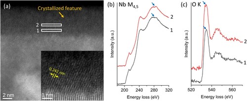
Although the NbOx layer shares chemical similarity in N-doped and non-doped samples, crystallized features are occasionally observed in the N-doped sample, as shown in Figure . A ∼5 nm nanocrystallized domain is captured in the N-doped sample. The spacing of the lattice fringes is ∼0.24 nm, close to the d-spacing of NbO 111 planes (0.2425 nm). EELS analysis also identified that the nanocrystal is highly possible to be NbO. The crystallized feature is not observed in the NbOx layer of the non-doped sample. Meanwhile, previous research indicates that the whole NbOx layer is removed during the nitrogen-doping treatment [Citation25]. Thus, the crystallized domains are formed during post-treatment in ambient conditions. This crystallization of NbO may be induced by the Nb surface strain relaxation [Citation45–47]. The compressive strain close to the Nb surface may also increase the hardness of the surface oxide layer [Citation48,Citation49].
Figure 5. Crystallized feature in NbOx amorphous layer. (a) HRSTEM image shows a crystalized feature in the amorphous layer, amplifying in the inset. (b-c) the EELS data from regions 1 and 2.
After comparing the microstructure and chemistry of non-doped and N-doped samples, we attribute the improved property of the N-doped sample to the following reasons. First, the thickness of the oxidation layer of the N-doped sample is 4.7 ± 0.6 nm, ∼20% less than that of the non-doped sample (5.8 ± 0.6 nm), resulting in lower surface resistance in the N-doped sample. The thickness reduction of the NbOx layer is related to the diffusion-control oxidation procedure. The Nb-oxide layer is removed at a high temperature before N-doping [Citation25]. Nitrogen atoms can diffuse into the octahedral interstitials of the Nb, causing a large residual in-plane compressive stress/strain near the surface [Citation35,Citation36], as indicated in our EBSD and backscattered image (Figures and ). The N-occupied interstitials and compressive stress/strain, impeding the diffusion of O atoms after treatment, can be explained by the atomic-scale and macroscopic views. In the atomic-scale view, the nitrogen atoms have already occupied some octahedral interstitial sites in the niobium lattice near the surface, reducing the available sites for subsequent oxygen diffusion in the N-doped Nb cavity. In the macroscopic view, the compressive stress/strain influences the flux of small gas atoms described by Fick’s first and second laws [Citation50,Citation51], limiting the diffusion rate and equilibrium oxygen concentration. Thus, the thickness of the NbOx layer is thinner in the N-doped sample compared with the non-doped sample. Meanwhile, strain relaxation induces a small amount of crystallization in the newly formed NbOx layer. The nano-domains potentially block the movement of O atoms by reducing the vacancies and interstitials in the amorphous layer [Citation52], limiting the mobility of free O atoms in the NbOx layer. Finally, since the H atoms will diffuse into either the octahedral or tetrahedral interstitial sites of Nb [Citation53], the existence of N interstitials blocks some of the diffusion pathways of the H atoms. Moreover, the interstitial N atoms can trap the H atoms [Citation54] and decrease hydrides’ thermodynamic stability [Citation30], reducing the likelihood of hydride precipitation at low temperatures [Citation55]. As a result, the cavities’ surface resistance decreases, and the Q-factor increases in various magnetic fields and frequencies by the N-doped surface treatment.
Conclusion
Our results help to understand the mechanisms of the property improvement in cavities by the N2 doping surface treatment. On the one hand, the N atoms diffuse into the Nb lattices, producing compressive stress/strain near the surface. The interstitial N atoms and compressive stress/strain impede the diffusion of oxygen atoms. We observed ∼20% thickness reduction of the oxidation layer in the N-doped sample compared with the non-doped sample. On the other hand, the interstitial N atoms could reduce the diffusion of hydrogen atoms and the stability of the hydrides at low temperatures. Since the amorphous oxidation layer and hydrides are two major components of the surface resistance, the N-doping surface treatment efficiently increases the Nb cavity’s performance. These findings will facilitate surface treatment optimization of the Nb SRF cavity.
Supplemental Material
Download MS Word (1.5 MB)Acknowledgments
This work was supported by the U.S. Department of Energy, Office of Science, National Quantum Information Science Research Centers, Superconducting Quantum Materials and Systems Center (SQMS) under the contract No. DE-AC02-07CH11359. All electron microscopy and related work were performed using instruments in the Sensitive Instrument Facility in Ames Lab. The Ames Laboratory is operated for the U.S. Department of Energy by Iowa State University under Contract No. DE-AC02-07CH11358.
Disclosure statement
No potential conflict of interest was reported by the author(s).
References
- Kneisel P. Radio-frequency superconductivity technology: Its sensitivity to surface conditions. Journal of Vacuum Science & Technology A: Vacuum, Surfaces, and Films. 1993;11:1575–1583.
- Dhakal P. Superconducting Radio Frequency Resonators for Quantum Computing: A Short Review. J Nep Phys Soc. 2021;7:1–5.
- Trenikhina Y, Romanenko A, Kwon J, et al. Nanostructural features degrading the performance of superconducting radio frequency niobium cavities revealed by transmission electron microscopy and electron energy loss spectroscopy. J Appl Phys. 2015;117:154507.
- Turneaure JP, Weissman I. Microwave Surface Resistance of Superconducting Niobium. J Appl Phys. 1968;39:4417–4427.
- Halbritter J, Kneisel P, Palmieri V, et al. Electric surface resistance RE(T, f, E⊥) of Nb/Nb2O5-y-interfaces and Q-drop of superconducting Nb cavities. IEEE Trans Appl Supercond. 2001;11:1864–1868.
- Barkov F, Romanenko A, Trenikhina Y, et al. Precipitation of hydrides in high purity niobium after different treatments. J Appl Phys. 2013;114:164904.
- Romanenko A, Barkov F, Cooley LD, et al. Proximity breakdown of hydrides in superconducting niobium cavities. Supercond Sci Technol. 2013;26:035003.
- Halbritter J. On the oxidation and on the superconductivity of niobium. Appl Phys A. 1987;43:1–28.
- Kim Y-J, Tao R, Klie RF, et al. Direct Atomic-Scale Imaging of Hydrogen and Oxygen Interstitials in Pure Niobium Using Atom-Probe Tomography and Aberration-Corrected Scanning Transmission Electron Microscopy. ACS Nano. 2013;7:732–739.
- Delheusy M, Stierle A, Kasper N, et al. X-ray investigation of subsurface interstitial oxygen at Nb/oxide interfaces. Appl Phys Lett. 2008;92:101911.
- Verjauw J, Potočnik A, Mongillo M, et al. Investigation of Microwave Loss Induced by Oxide Regrowth in High- Q Niobium Resonators. Phys Rev Applied. 2021;16:014018.
- Tao R, Todorovic R, Liu J, et al. Electron energy-loss spectroscopy study of metallic Nb and Nb oxides. J Appl Phys. 2011;110:124313.
- Nico C, Monteiro T, Graça MPF. Niobium oxides and niobates physical properties: Review and prospects. Prog Mater Sci. 2016;80:1–37.
- Cava RJ, Batlogg B, Krajewski JJ, et al. Electrical and magnetic properties of Nb2 O5 − δ crystallographic shear structures. Phys Rev B. 1991;44:6973–6981.
- Proslier T, Zasadzinski JF, Cooley L, et al. Tunneling study of cavity grade Nb: Possible magnetic scattering at the surface. Appl Phys Lett. 2008;92:212505.
- Romanenko A, Pilipenko R, Zorzetti S, et al. Three-Dimensional Superconducting Resonators at T < 20 mK with Photon Lifetimes up to τ = 2 s. Phys Rev Applied. 2020;13:034032.
- Antoine CZ, Berry S.. H in Niobium: origin and method of detection. In: AIP Conference Proceedings. Vol. 671. Virginia (USA): American Institute of Physics; July 2003. p. 176–189.
- Barkov F, Romanenko A, Grassellino A. Direct observation of hydrides formation in cavity-grade niobium. Phys Rev ST Accel Beams. 2012;15:122001.
- Knobloch J. The “Q disease” in superconducting niobium RF cavities. In: AIP Conference Proceedings. Vol. 671. Virginia (USA): American Institute of Physics; July 2003. p. 133–150..
- Ciovati G. Effect of low-temperature baking on the radio-frequency properties of niobium superconducting cavities for particle accelerators. J Appl Phys. 2004;96:1591–1600.
- Saito K, Noguchi S, Ono M, et al. Superiority of electropolishing over chemical polishing on high gradients. Part Accel. 1998;60:193–217.
- Cooper CA, Cooley LD. Mirror-smooth surfaces and repair of defects in superconducting RF cavities by mechanical polishing. Supercond Sci Technol. 2013;26:015011.
- Romanenko A, Grassellino A. Dependence of the microwave surface resistance of superconducting niobium on the magnitude of the rf field. Appl Phys Lett. 2013;102:252603.
- Dhakal P. Nitrogen doping and infusion in SRF cavities: A review. Physics Open. 2020;5:100034.
- Grassellino A, Romanenko A, Sergatskov D, et al. Nitrogen and argon doping of niobium for superconducting radio frequency cavities: a pathway to highly efficient accelerating structures. Supercond Sci Technol. 2013;26:102001.
- Grassellino A, Romanenko A, Trenikhina Y, et al. Unprecedented quality factors at accelerating gradients up to 45 MVm −1 in niobium superconducting resonators via low temperature nitrogen infusion. Supercond Sci Technol. 2017;30:094004.
- Reece CE, Palczewski AD, Xiao B. An analysis of the temperature and field dependence of the RF surface resistance of nitrogen-doped niobium SRF cavities with respect to existing theoretical models (No. JLAB-ACC-15-2050; DOE/OR/23177-3353). Thomas Jefferson National Accelerator Facility (TJNAF), Newport News, VA, USA; 2015.
- Martinello M, Bice DJ, Boffo C, et al. Q-factor optimization for high-beta 650 MHz cavities for PIP-II. J Appl Phys. 2021;130:174501.
- Martinello M, Checchin M, Romanenko A, et al. Field-Enhanced Superconductivity in High-Frequency Niobium Accelerating Cavities. Phys Rev Lett. 2018;121:224801.
- Garg P, Balachandran S, Adlakha I, et al. Revealing the role of nitrogen on hydride nucleation and stability in pure niobium using first-principles calculations. Supercond Sci Technol. 2018;31:115007.
- Ford DC, Cooley LD, Seidman DN. Suppression of hydride precipitates in niobium superconducting radio-frequency cavities. Supercond Sci Technol. 2013;26:105003.
- Schubert U, Metzger H, Peisl J. Diffuse X-ray scattering from interstitial nitrogen in niobium. I. Huang diffuse scattering. J Phys F: Met Phys. 1984;14:2457–2466.
- Oh J, Cha H, Kim T, et al. Low angle boundary migration of shot-peened pure nickel investigated by electron channeling contrast imaging and electron backscatter diffraction. Microsc Res Tech. 2019;82:849–855.
- Wright SI, Nowell MM, Field DP. A Review of Strain Analysis Using Electron Backscatter Diffraction. Microsc Microanal. 2011;17:316–329.
- Bourke MAM, Rangaswamy P, Holden TM, et al. Complementary X-ray and neutron strain measurements of a carburized surface. Mater Sci Eng A. 1998;257:333–340.
- Palaniradja K, Alagumurthi N, Soundararajan V. Residual Stresses in Case Hardened Materials. TOMSJ. 2010;4:92–102.
- Liu G, Yu JC, Lu G(, et al. Crystal facet engineering of semiconductor photocatalysts: motivations, advances and unique properties. Chem Commun. 2011;47:6763.
- Arfaoui I, Cousty J, Guillot C. A model of the NbOx≈1 nanocrystals tiling a Nb(110) surface annealed in UHV. Surf Sci. 2004;557:119–128.
- Uehara Y, Fujita T, Iwami M, et al. Single NbO nano-crystal formation on low temperature annealed Nb(001) surface. Surf Sci. 2001;472:59–62.
- Koch CC, Scarbrough JO, Kroeger DM. Effects of interstitial oxygen on the superconductivity of niobium. Phys Rev B. 1974;9:888–897.
- Kirchheim R. Metals as sinks and barriers for interstitial diffusion with examples for oxygen diffusion in copper, niobium and tantalum. Acta Metall. 1979;27:869–878.
- Findlay SD, Shibata N, Sawada H, et al. Dynamics of annular bright field imaging in scanning transmission electron microscopy. Ultramicroscopy. 2010;110:903–923.
- Leapman RD, Hunt JA. Comparison of detection limits for EELS and EDXS. Microsc Microanal Microstruct. 1991;2:231–244.
- Bach D. (2009). EELS investigations of stoichiometric niobium oxides and niobium-based capacitors. Available from: https://publikationen.bibliothek.kit.edu/1000012945.
- Shao X, Nilius N, Myrach P, et al. Strain-induced formation of ultrathin mixed-oxide films. Phys Rev B. 2011;83:245407.
- Akbashev AR, Plokhikh AV, Barbash D, et al. Crystallization engineering as a route to epitaxial strain control. APL Mater. 2015;3:106102.
- Yan Z, Hu Y, Song K, et al. Vickers-indentation-induced crystallization in a metallic glass. Appl Phys Lett. 2015;106:101909.
- Wang L, Bei H, Gao YF, et al. Effect of residual stresses on the hardness of bulk metallic glasses. Acta Mater. 2011;59:2858–2864.
- Ahn S, Park S-Y, Kim Y-C, et al. Surface residual stress in soda-lime glass evaluated using instrumented spherical indentation testing. J Mater Sci. 2015;50:7752–7759.
- Van Leeuwen HP. The kinetics of hydrogen embrittlement: A quantitative diffusion model. Eng Fract Mech. 1974;6:141–161.
- Toribio J, Elices M. Influence of residual stresses on hydrogen embrittlement susceptibility of prestressing steels. Int J Solids Struct. 1991;28:791–803.
- Lazarus D. Diffusion in Crystalline and Amorphous Solids. MRS Proc. 1985;57:297.
- Makenas BJ, Birnbaum HK. Phase changes in the niobium-hydrogen system—II. low temperature hydride phase transitions. Acta Metall. 1982;30:469–481.
- Pfeiffer G, Wipf H. The trapping of hydrogen in niobium by nitrogen interstitials. J Phys F: Met Phys. 1976;6:167–179.
- Makenas BJ, Birnbaum HK. Phase changes in the niobium-hydrogen system I: Accommodation effects during hydride precipitation. Acta Metall. 1980;28:979–988.