
 ?Mathematical formulae have been encoded as MathML and are displayed in this HTML version using MathJax in order to improve their display. Uncheck the box to turn MathJax off. This feature requires Javascript. Click on a formula to zoom.
ABSTRACT
The two-dimensional (2D) materials-based tunneling field-effect transistors (TFETs) suffer from low driving currents. In contrast to the prevailing wisdom that defects are detrimental, we proposed to harness the ubiquitous defects in MoS2 to overcome the problem of the low on-state current in TFET. The existence of certain molybdenum-related vacancies and sulfur vacancy in appropriate positions confers the higher driving currents without compromising the low-power benefits. Such performance enhancements are related to the defect-assisted resonant Zener tunneling mechanism introduced by the mid-gap states of the vacancy defects. These unveiled hidden defect benefits could provide new opportunities for boosting the performance of 2D TFETs.
GRAPHICAL ABSTRACT
IMPACT STATEMENT
The defect-assisted resonant Zener tunneling mechanism in TFET introduced by the mid-gap states of the vacancies in MoS2 is beneficial for enhancing the on-state current.
1 Introduction
Integrated circuit (IC) technology is advancing in the direction of miniaturization, ultrahigh speed, low-power consumption and high performance. Field-effect transistor (FET) is the most basic working unit in ICs, and the reduction of its physical size guarantees the exponential development of chip integration and the continuous improvement of the chip performance [Citation1,Citation2]. However, the resulting short channel effects [Citation3–4] and other quantum effects may degrade the performance of the conventional FETs and therefore new design space has to be explored. For a FET, the subthreshold swing SS = dVG/dlog10ID is an important figure of merit that reflects the steepness of the slope of the I-V transfer curve upon the transition between the off and on state, where VG is the gate voltage and ID is the drain current. In a conventional FET, the SS cannot be smaller than 60 mV/decade at room temperature because of the avoidable thermionic emission of carriers in the off-state (known as the Boltzmann limit) [Citation5], preventing the device power from further reduction. To enable denser integration and power up a lot more computing cores, it is necessary to use new devices with steeper subthreshold slopes.
In early this century, a new type of FET, the tunnel field-effect transistor (TFET), was proposed utilizing the Zener tunneling mechanism rather than thermal injection [Citation6–9]. The electron (hole) carrier transport in an n-type (p-type) TFET is from valence (conduction) band of p-doped (n-doped) source through the source–channel energy barrier via tunneling to the conduction (valence) band of channel, i.e. the band-to-band tunneling (BTBT). Because of the tunneling nature of carrier transport, SS less than 60 mV/decade and lower subthreshold leakage current can be achieved. However, due to the low transparency of the tunneling barrier, TFET suffers from low on-state current, usually orders of magnitude lower than that of the conventional MOSFET, which becomes a severe obstacle for TFET application in high performance IC. In the past decades, significant efforts have been made to investigate the solutions to the enhancement of the on-state current, such as the use of thin-body TFET structure to improve gate controllability, the use of low bandgap source, and the use of low-bandgap and small reduced-effective-mass channel materials [Citation10-15].
Two-dimensional (2D) semiconductors, such as MoS2, are emerging channel materials for future FETs [Citation16,Citation17]. Their natural ultra-thin bodies can improve gate controllability, making them also attractive for TFETs. Unfortunately, most of the experimentally fabricated 2D semiconductors have severely degraded carrier mobilities, impeding the realization of high on-state current [Citation18–20]. Unlike most conventional semiconductors with band-like transport [Citation21–24], the carrier transport in MoS2 has often been found to exhibit the characteristics of variable-range hopping [Citation25–27]. This unique property has been associated with the existence of rich defects. Direct observations of various vacancy defects have been reported in monolayer MoS2 grown by chemical vapor deposition method [Citation28]. S vacancies (VS) are common in all samples. Mo-related vacancies are also abundant, usually presented as VMoS3 defect complexes, each with three VS around a VMo.
In contrast to the common wisdom that defects are detrimental, Zhang et al. [Citation29] recently found that by tailoring the sulfur vacancy defects to an optimum density of 4.7% in monolayer MoS2, an unusual mobility enhancement can be obtained and a record-high carrier mobility is achieved. In this paper, we report more than two orders of magnitude enhancements of the on-state currents in TFETs in the presence of VMo, VS and VMoS3. This is found to be due to the inelastic defect-assisted resonant Zener tunneling. Our findings suggest a generic defect engineering strategy for boosting the performance of 2D TFETs for high-performance ICs.
2. Methods
The density functional theory and the non-equilibrium Green’s function method implemented in ATK 2020 package were employed [Citation30]. The double-ζ polarized basis set and Local Density Approximation exchange correlation were adopted. The k-point samples were 1 × 2 × 2 and 1 × 7 × 153 during the electronic structure and device transport calculations, respectively. A 20 Å vacuum layer was used in the x-direction, and the transport direction was along the z-axis. The energy difference was converged to 10−5 eV/atom, and the maximum residual force was converged to 0.01 eV/Å. The real space mesh cutoff energy was set at 75 Hartree, and the temperature was 300 K. The driving current at a given bias voltage VSD and gate voltage VG was calculated by the special thermal displacement-Landauer method [Citation31–33]:
(1)
(1)
where T (E, Vds, Vg) is the transmission coefficient, fS and fD are the Fermi–Dirac distribution functions for the source and drain, μS and μD are the electrochemical potentials.
3. Results and discussion
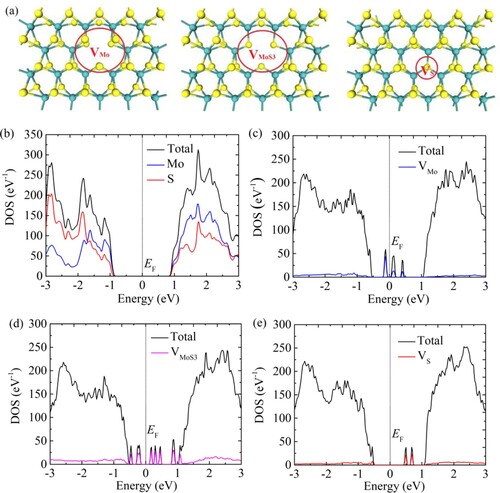
The calculated lattice constant of monolayer MoS2 is 3.11 Å, and the LDA band gap is 1.83 eV, in reasonable agreement with the experiments [Citation34]. Experimental observations have shown the existence of VS, VMo and VMoS3 in MoS2 [Citation28,Citation35], whose atomic structures are shown in Figure (a). The densities of states (DOSs) of the defect-free MoS2 and defective MoS2 are shown in Figure (b–e). It is seen that VMo, VMoS3 and VS can all introduce mid-gap states, but with varying energy distributions. In particular, the states of VMo tend to locate in the middle of the gap, while the states of VS locate near the edge of the conduction band. As expected, the states of VMoS3 are more broadly distributed in energy, from near the valence band edge to near the conduction band edge.
Figure 1. (a) Schematic representation of atomic structures of various common defects in MoS2, a 1 × 4 × 8 orthorhombic supercell is used for DOS calculation. Electronic density of states of (b) defect-free MoS2, and defective MoS2 containing (c) VMo, (d) VMoS3 or (e) VS. The DOSs for vacancies are obtained by the projection of density of states on particular atoms near the vacancy defects.
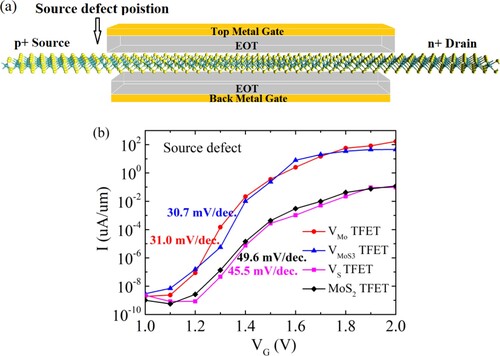
Next, we simulate the carrier transport phenomena in three dual-gated MoS2 homojunction TFETs, each containing one of these three types of point defects in the source region near the source–channel interface, as schematically shown in Figure (a). For the device model, the source and drain electrodes are p-type and n-type electrostatic doped by using the atomic compensation charges method, the doping concentration is 2.2 × 1013 cm−2. The length of the intrinsic channel region is 7.9 nm, the equivalent oxide thickness (EOT) was set to be 0.49 nm, and the dielectric constant was 3.9. Here, EOT indicates how thick a silicon oxide film would need to be to produce the same effect as the high-k material being used. In total, there are 492 atoms in a TFET model device. Each of the defective models contains only one defect on either the source side or the channel side of the source–channel heterojunction, which is equivalent to a defect density of 2 × 1013 cm-2 as normalized by the channel surface area. This defect density is comparable to that measured in experiment [Citation28,Citation35]. In addition, because there is at most one defect in the channel of the simulated device and the channel length is much greater than the localization length estimated from the variable-range hopping model [Citation27], the mechanism of conduction in the channel of the simulated device is actually assumed to be band-like transport. In fact, band-like transport behavior can be observed in the high-carrier density linear region if the devices are carefully prepared and measured under conditions that minimize surface adsorbates [Citation21–24].
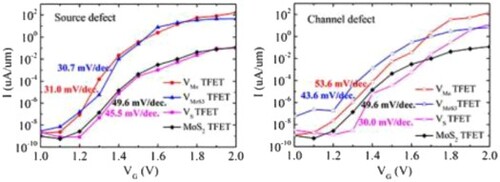
Figure 2. (a) Atomic configuration of monolayer MoS2 TFET with a vacancy defect in the source region near the source-channel interface. (b) Comparison of the transfer characteristics between the defect-free MoS2 TFET and defect-containing MoS2 TFETs. The drain bias is set to be VSD = −0.69 V.
The calculated transfer curves for the defect-free and defect-containing devices are shown in Figure (b). Compared to the defect-free device, the on-state currents of the VMo and VMoS3-containing devices are larger by nearly three orders of magnitude, while the off-state currents are only slightly higher. The SS values are calculated to be 31.0 mV/decade for VMo-containing TFET and 30.7 mV/decade for VMoS3-containing TFET. On the other hand, both the on-state and off-state currents of the VS-containing device are comparable to those of the defect-free device.
To better understand the origins of the performance enhancements achieved by introducing VMo and VMoS3 into the source regions, analyses of the device densities of states (DDOSs) of the defect-free MoS2 TFET (Figure (a)), and of the devices containing VS, VMo and VMoS3 defects (Figure (b–d)) at their on-state are conducted. One can see from Figure (b,c) that there are many mid-gap states within the tunneling window localized at the source–channel interface. It is therefore expected that the defect-assisted resonant Zener tunneling can occur. To verify this hypothesis, we examine the atomic projected densities of states (PDOSs) and the transmission coefficients (T(E)s) in the on-state MoS2 TFETs without and with point defects, as shown in Figure (e–h). As can be seen, the source valance band (VB) and the channel conduction band (CB) overlap each other, opening up the BTBT window. Compared to the defect-free TFET (Figure (e)), one can find in Figure (f) that the existence of the VMo defect dramatically increases the T(E), with the energies where T(E) peak coinciding with the VMo defect energy levels. This indicates that the resonant tunneling occurs as assisted by the mid-gap defect states. Similar phenomena can be found in the case of VMoS3, as shown in Figure (g). Compared to VMo and VMoS3, the existence of VS does not increase the on-state current (Figure (b)). This can be understood by noticing that the VS mid-gap states locate outside the BTBT window, as expected from the high energy positions of the VS defect states near the CB edge of the source MoS2 (Figure (d,h)).
Figure 3. Device densities of states of MoS2 TFETs (a) without defect and with (b) VMo, (c) VMoS3 and (d) VS defects in the source regions. Atomic projected densities of states and the transmission coefficients in the MoS2 TFETs (e) without and with (f) VMo, (g) VMoS3 and (h) VS defects. The overlapped region between the source valance band and channel conduction band defines the BTBT window.
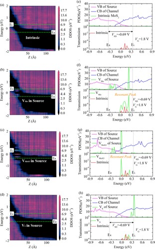
Figure 4. (a) Atomic configuration of monolayer MoS2 TFET with a vacancy defect located in the channel region near the source-channel interface. (b) Comparison of the transfer characteristics between the defect-free MoS2 TFET and defect-containing MoS2 TFETs. The drain bias is set to be VSD = −0.69 V.
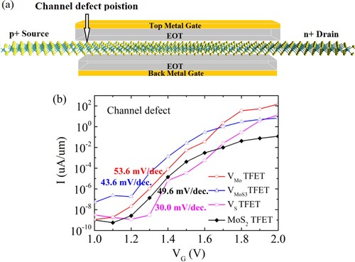
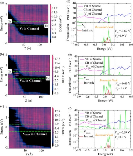
Given the above findings and considering the two facts that the tunneling window is formed between the source VB edge and channel CB edge, and the energy positions of the VS defect states are near the CB edge of MoS2, it is natural to ask whether or not creating a VS defect in the channel region near the source–channel interface can enable defect-assisted tunneling and achieve high on-state current. To answer this question, TFET models without and with VS, VMo and VMoS3 defects in the channel regions near the source–channel interface are built, as shown in Figure (a).
Figure (b) shows the transfer characteristics of a monolayer MoS2 TFET with such a VS located in the channel region. In line with our expectation, the TFET shows nearly two orders of magnitude increase in the on-state current compared to that of the defect-free device, with a low SS of 30 mV/decade. The DDOS, PDOS as well as the tunneling transmission coefficient (Figure (a,d)) further show that the energies where the transmission coefficient peaks coincide with the mid-gap defect levels within the BTBT window, which is a key signature of the resonant Zener tunneling. The transfer characteristics of MoS2 TFETs with VMo and VMoS3 defects located in the channel region are also shown in Figure (b). It is seen that these two devices have on-state currents larger than that of the defect-free device as well, both with sub-60 mV/decade SSs. Figure shows that there are also resonant mid-gap defect states within the BTBT windows whose energy levels coincide with those at which the transmission coefficients peak. The abilities of the VMo and VMoS3 defects that locate at either position, i.e. in the source region or in the channel region, to assist BTBT can be understood as due to their near-middle of the gap or broadly distributed energy levels. The above findings provide new insights into the design of MoS2 TFETs by engineering suitable defects into appropriate positions to overcome the problems of limited on-state currents in TFETs. Further improvements may be through other materials engineering approaches, such as the use of low-bandgap source, as recently demonstrated in experiment where record high I60 (the current where SS becomes 60 mV/decade) was achieved [Citation14]. In addition, the effects of defect density on VMo-containing and VS-containing devices have been discussed in the Supporting Information.
Figure 5. Device density of states of MoS2 TFETs with (a) VS, (b) VMo, and (c) VMoS3 defects in the channel region. Atomic projected density of states and the transmission coefficients in the MoS2 TFETs with (d) VS, (e) VMo, and (f) VMoS3 defects.
Accordingly, we envision that the main practical challenge to implement this approach effectively is to precisely create the desired defects and control their positions. As for position-selective creation of defects, with the advancement of scanning transmission electron microscopy (STEM), the sub-angstrom-sized electron probe guarantees single-atom accuracy of the electron–matter interaction and allows electron-beam irradiation to precisely create defects in 2D MoS2 [Citation36]. Recently, Zhang et al. [Citation29] also reported a method to tailor a single vacancy in 2D MoS2, involving a mild anneal in the high-pure hydrogen atmosphere. As for the creation of VMo and VMoS3 defects with higher formation energies compared to that of VS defect, non-equilibrium growth techniques can be used, such as rapid cooling. It has also been found experimentally that under prolonged electron-beam irradiation VMoS3 can be generated, presumably via ionization, beam-induced chemical etching, ballistic displacement, or catalyzed by hydrocarbon surface contamination [Citation28,Citation36].
4. Conclusions
We have demonstrated that engineering defects in MoS2 can be beneficial for assisting the BTBT process in the operating of the TFET. In particular, by introducing defects, whose mid-gap states lie close to conduction band edge, such as VS, into the channel region near the source–channel interface, or by introducing defects, whose mid-gap states lie close to the valence band edge, into the source region near the source–channel interface can enhance the on-state current of an n-type TFET because the mid-gap defect levels fall within the BTBT window and therefore can assist tunneling. Defects that have near-middle of the gap states or broadly distributed energy levels, such as VMo and VMoS3, can be engineering into both the source region and the channel region for the same purpose. The arguments developed in this work are very general and could be readily extrapolated to p-type TFETs (opposite ‘defect level-defect position' design rule) and other materials systems. In our simulated cases, the introduction of suitable defects at appropriate positions enhances the driving currents without compromising the low-power benefits. Our work provides a new strategy to overcome the problem of the limited on-state currents in TFETs.
Supplemental Material
Download MS Word (619.6 KB)Disclosure statement
No potential conflict of interest was reported by the author(s).
Additional information
Funding
References
- Moore GE. (2006). Cramming more components onto integrated circuits, Reprinted from Electronics, volume 38, number 8, April 19, 1965, pp.114 ff., IEEE Solid-State Circuits Society Newsletter 11, 33.
- International roadmap for devices and systems (IRDSTM). (2020 edition). https://irds.ieee.org/editions/2020.
- Godoy A, Lopez-Villanueva JA, Jimenez-Tejada JA, et al. A simple subthreshold swing model for short channel MOSFETs. Solid State Electron. 2001;45:391.
- Oh SH, Monroe D, Hergenrother J. Analytic description of short-channel effects in fully-depleted double-gate and cylindrical, surrounding-gate MOSFETs. IEEE Electron Device Lett. 2000;21:445.
- Taur Y, Ning TH. Fundamentals of modern VLSI devices. Cambridge (England): Cambridge University Press; 1998.
- Ionescu AM, Riel H. Tunnel field-effect transistors as energy-efficient electronic switches. Nature. 2011;479:329.
- Avci UE, Morris DH, Young IA. Ieee journal of the electron devices society information for authors. IEEE J Electron Dev Soc. 2015;3:C3.
- Zhang Q, Zhao W, Seabaugh A. Low-subthreshold-swing tunnel transistors. IEEE Electron Device Lett. 2006;27:297.
- Zener C. (1932). Proceedings of the Royal Society A pp. 696.
- Sarkar D, Xie X, Liu W, et al. A subthermionic tunnel field-effect transistor with an atomically thin channel. Nature. 2015;526:91.
- Roy T, Tosun M, Xi C, et al. Dual-Gated MoS2/WSe van der Waals tunnel diodes and transistors. Acs Nano. 2015;9:2071.
- Gong C, Zhang HJ, Wang WH, et al. Band alignment of two-dimensional transition metal dichalcogenides: application in tunnel field effect transistors. Appl Phys Lett. 2013;103:329.
- Verhulst AS, Vandenberghe WG, Maex K, et al. Boosting the on-current of a n-channel nanowire tunnel field-effect transistor by source material optimization. J Appl Phys. 2008;104:064514.
- Kim S, Myeong G, Shin W, et al. Thickness-controlled black phosphorus tunnel field-effect transistor for low-power switches. Nat Nanotechnol. 2020;15:203.
- Zhou WH, Qu HZ, Guo SY, et al. Dependence of tunneling mechanism on two-dimensional material parameters: a high-throughput study. Phys Rev Appl. 2022;17:6.
- Liu Y, Duan X, Shin HJ, et al. Promises and prospects of two-dimensional transistors. Nature. 2021;591:7848.
- Liu C, Chen H, Wang S, et al. The switch is on. Nat Nanotechnol. 2020;15:7.
- Yu ZH, Ong ZY, Li SL, et al. Analyzing the carrier mobility in transition-metal dichalcogenide MoS2 field-effect transistors. Adv Mater. 2017;27:1604093.
- Radisavljevic B, Radenovic A, Brivio J, et al. Single-layer MoS2 transistors. Nat Nanotechnol. 2011;6:147.
- Baugher BWH, Churchill HOH, Yang Y, et al. Intrinsic electronic transport properties of high-quality monolayer and bilayer MoS2. Nano Lett 2013;13:4212.
- Jariwala D, Sangwan VK, Late DJ, et al. Band-like transport in high mobility unencapsulated single-layer MoS2 transistors. Appl Phys Lett. 2013;102:173107.
- Schmidt H, Wang SF, Chu LQ, et al. Transport properties of monolayer MoS2 grown by chemical vapor deposition. Nano Lett 2014;14:1909.
- Wan Y, Li E, Yu ZH, et al. Low-defect-density WS2 by hydroxide vapor phase deposition. Nat Commun. 2022;13:4149.
- Cheng J, Poehler S, Laskar M, et al. Temperature dependent carrier transport in few-layered MoS2: from hopping to band transport. J Phys D: Appl Phys. 2022;55:195109.
- Qiu H, Xu T, Wang ZL, et al. Hopping transport through defect-induced localized states in molybdenum disulphide. Nat Commun. 2013;4:2642.
- Zhu WJ, Low T, Lee YH, et al. Electronic transport and device prospects of monolayer molybdenum disulphide grown by chemical vapour deposition. Nat Commun. 2014;5:3087.
- Ovchinnikov D, Allain A, Huang YS, et al. Electrical transport properties of single-layer WS2. Acs Nano. 2014;8:8174.
- Zhou W, Zou XL, Najmaei S, et al. Intrinsic structural defects in monolayer molybdenum disulfide. Nano Lett. 2013;13:2615.
- Zhang XK, Liao QL, Liu ZKBS, et al. Hidden vacancy benefit in monolayer 2D semiconductors. Adv Mater. 2021;33:7.
- Brandbyge M, Mozos JL, Ordejon P, et al. Density-functional method for nonequilibrium electron transport. Phys Rev B. 2002;65:16.
- Datta S. Electronic transport in mesoscopic systems. Cambridge: Cambridge University Press; 1995.
- Gunst T, Markussen T, Palsgaard MLN, et al. First-principles electron transport with phonon coupling: large scale at low cost. Phys Rev B. 2017;96:16.
- Jiang JW, Park HS, Rabczuk T. Molecular dynamics simulations of single-layer molybdenum disulphide (MoS2): Stillinger-Weber parametrization, mechanical properties, and thermal conductivity. J Appl Phys. 2013;114:6.
- Mak KF, Lee C, Hone J, et al. Atomically thin MoS2: a new direct-gap semiconductor. Phys Rev Lett. 2010;105:13.
- Hong JH, Hu ZX, Probert M, et al. Exploring atomic defects in molybdenum disulphide monolayers. Nat Commun. 2015;6:6293.
- Liang QJ, Zhang Q, Zhao XX, et al. Defect engineering of two-dimensional transition-metal dichalcogenides: applications, challenges, and opportunities. ACS Nano. 2021;15:2165.