
 ?Mathematical formulae have been encoded as MathML and are displayed in this HTML version using MathJax in order to improve their display. Uncheck the box to turn MathJax off. This feature requires Javascript. Click on a formula to zoom.
ABSTRACT
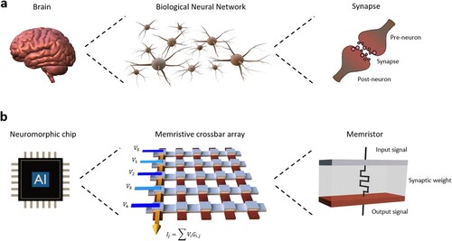
Neuromorphic computing based on brain-inspired frameworks has shown its potential to perform computation with remarkable power and speed efficiency. The spintronic device has been considered a promising candidate for neuromorphic computing because of its intrinsic non-volatility, ultrafast switching dynamics and scalability. This article will review the current status of neuromorphic computing techniques employing spintronic materials and devices. We will begin with a concise introduction to the biological structure of neurons and then go through several important models of artificial neural networks. The revolutionary breakthroughs of spintronic-based neuromorphic computation will be demonstrated together with their challenges and outlook.
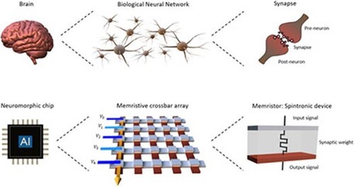
GRAPHICAL ABSTRACT
IMPACT STATEMENT
This paper will systematically review the status of neuromorphic computing techniques employing spintronic materials and devices. After reading this article, readers can grasp the revolutionary breakthroughs of spintronic-based neuromorphic computation.
1. Introduction
Playing Go games was absolutely a milestone for modern computer technology [Citation1], because, unlike other chess games, Go would yield the most possible events, i.e. 1919 playable points with 3 different possibilities for every single play, which makes it almost impossible for conventional computers to calculate all viable movements in a very limited time. Quantum computing may be one of the possible solutions to solve this issue; however, the quantum technology so far is still at the incubation stage. It drives current computing-related research to look for an upgrade approach to accelerate the computing speed to meet the rising requirements like the Go game. Neuromorphic computing-based artificial intelligence (AI) appears to be an ideal alternative because it mimics how a human brain behaves. Although the advantages of AI techniques look promising, some critical issues still emerge and can be ascribed to two perspectives [Citation2]:
Speed: During a certain process of information, central processing units (CPUs) require devices with long- and short-term memory to store and use the information back and forth. This gives rise to the unavoidable delay between computing and storage devices unless in-memory computing is realized.
Power consumption: Modern AI technology can perform multiple data processes with a relatively high speed; however, computing based on complementary metal–oxide-semiconductor transistor (CMOS) circuits often needs a complex array architecture to accomplish the assigned tasks, leading to tremendous energy consumption.
Technically, a dilemma exists for accelerating calculation speed and simultaneously reducing power consumption because high calculation speed is often fulfilled by a colossal system, thus, accompanying high power consumption. To conquer this dilemma, new approaches out of the conventional scope were proposed in recent years, including materials, circuits, algorithms, system architectures, etc. [Citation3]. Various approaches to the applications of AI and neuromorphic computing have been demonstrated using ferro-electric materials [Citation4], resistive switching materials [Citation5], analog very-large-scale integration designs [Citation6] and spike-based algorithms on both circuit and hardware [Citation7]. Among all demonstrations, the magneto-resistive random-access memory (MRAM) has been considered an ideal candidate to realize low power consumption with a high speed for neuromorphic computing because of its non-volatility and ultrafast switching dynamics [Citation8]. These characteristics, together with the non-trivial spintronic properties via spin-transfer torque (STT), voltage control magnetic anisotropy (VCMA), spin-torque oscillator or spin–orbit torque (SOT), further polish various facets of MRAM to be applied for different neuromorphic applications. Even benefitted from the promising nano-scalability and read/write speed at (sub)-GHz scale, MRAM has distinguished itself from other memories and is capable of participating in advanced computing technologies [Citation9,Citation10].
In this review, we will show the state-of-the-art neuromorphic applications utilizing spintronic materials and devices. The core structure of this article focuses on how to turn a solid-state device to be a bionic neuron to perform specific tasks in computing. In Section 2, we will begin with a concise introduction to the properties of biological neurons and the way to bridge them to the artificial neurons composed of solid-state devices. Section 3 will demonstrate the architecture of how the current AI works in different types of neural networks along with their pros and cons. Additionally, we focus on the development of novel computing schemes and hardware to overcome the limitations of current computing technology. To realize a high calculation speed and energy efficiency, Section 4 will report the current neuromorphic computing based on the spintronics of STT, VCMA and stochastic cells. In Section 5, we will present SOT-based neuromorphic devices, of which remarkable stability and spike-timing dependent-plasticity (STDP) at a nanosecond scale open a new page for neuromorphic computing technology. In Section 6, we will come up with the challenges and outlook for materials and devices to be implemented for the last mile toward a spintronic artificial neural network (ANN).
2. Biological neurons and synapses
The brain is the most complex organ in the human body, which gathers tens of thousands of neurons to process signal delivery for our daily life. Composed of dendrites, soma and axons, neurons can receive signals/stimuli, proceed with the analysis and then deliver messages to the following acceptors through axons. Signal transfer occurs when neurons start to inter-communicate by passing the electrical potential on the membrane through ion channels.
2.1. How do neurons and synapses work?
To explain how neurons work, we would like to briefly describe how neurons respond to stimuli and deal with signal transfer. A cell of a neuron is composed of three parts: dendrites, soma and axon, as shown in Figure (a). A typical neuron cell would have many dendrites but only one axon. Dendrites are channels where stimuli are input into a neuron and the axon is the output passage of a neuron. Soma, which refers to the main cell body of a neuron, is responsible for collecting stimuli and deciding whether output signals should be fired. Signals in a neuron are delivered through changes in electrical potential, denoted as an action potential. When a neuron decides to fire out a signal, it generates an action potential passing along the membrane of the axon and arriving at a synapse, which is the joint between the axon and the dendrite of the next neuron. To generate changes in action potential responding to stimuli, various ions need to be exchanged through the membrane of neural cells, which comprises voltage-gate calcium channels (Cav), voltage-gate sodium channels (Nav), voltage-gate potassium channels (Kv) and other specialized chemical acceptors such as N-Methyl-D-aspartic acid (NMDA) acceptors [Citation11]. Nav and Kv are usually found in all parts of neurons including presynaptic terminals, while Cav is commonly located at pre- and post-synaptic terminals.
Figure 1. (a) Typical structure of a neuron composed of dendrites, soma, axon and synaptic terminals. (b) Illustration for action potential of a neuron. (c) Schematic diagram for the four phases of the change on membrane potential. Blue and red dots are Na+ and K+ ions, respectively. Yellow, green and orange channels are Na+ channels, K+ channels and Na+/K+ pumps, respectively.
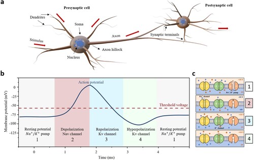
Figure (b) shows a typical action potential profile of a neuron with four different phases, corresponding to the schematic diagrams in Figure (c). Ion concentrations inside and outside of a neuron determine the state of membrane potential. When no stimulus or no chemical signal is treated, a neuron sustains at its resting potential (−70 mV), as shown in phase 1 of Figure (b). At this stage, the resting potential originates from the concentration difference between K+ inside and Na+ outside the neuron, at which we refer to a polarization state. When a neuron receives excitatory signals, the channels of Na+ ions in the membrane allow more Na+ ions to permeate into the cell, leading to potential increment. When the potential surpasses a threshold voltage, the local Nav will be fully opened to drive in a large amount of Na+ ions, which we refer to as a depolarization state, as shown in phase 2 of Figure (b). To balance the excess cations inside the membrane, K+ ions will be released through the Kv outward together with the suppressed Na+ migration through the Nav inward, thus leading to a potential drop as a repolarization state as phase 3 of Figure (b). Because the Kv is less sensitive to respond to the potential variation during the cation exchange, K+ is often over-released although the potential has been recovered to the resting state, at which we refer to a hyperpolarization state as phase 4 in Figure (b). Once the hyperpolarization occurs, the Na+/K+ pumps are subsequently activated to turn the potential back to the resting state to complete a cycle for the next action potential. Biologically, the height of action potential is determined by the concentration of Na+/K+ so any modification on Na+/K+ concentration would lead to variations on the action potential, serving as the origin of intrinsic plasticity of a neuron, enabling the modification of signal when it is delivered.
In addition to Na+ and K+ ion channels, Ca2+ ions are active around synapses through Cav. When an action potential reaches a synaptic terminal, it would activate Cav in this area. The functionality of Cav takes charge of the formation of exocytosis and releases neurotransmitters to post-synaptic terminals. These bubble-like neurotransmitters would flow through the area of the synapse and arrive at the post-synaptic terminal and subsequently trigger another action potential in the following neuron. Any disturbance or variation in the concentration of chemicals around the synapse could lead to the modification of the signal, which is the common origin of synaptic plasticity. To summarize, biological neurons can reshape signals (information) during delivery due to intrinsic and synaptic plasticity.
2.2. Learning process in neurons
A synapse is where information can be modified while transferring signals between neurons. Synaptic plasticity is, therefore, regarded as the most critical component for biological learning and memory. In terms of the timescale of plasticity response, synaptic plasticity can be categorized into short-term synaptic plasticity (STSP) and long-term synaptic plasticity (LTSP). If the plasticity results in an increase or decrease of membrane potential, it is referred to as excitatory post-synaptic potential (EPSP) or inhibitory post-synaptic potential (IPSP), respectively.
STSP is a temporary modification of action potential between terminals with a Ca2+ concentration gradient. Paired-pulse facilitation is one of the common triggers for an STSP [Citation12], that is, if two action potentials reach the synapse gaped within a very short time around tens of milliseconds, the exceeding Ca2+ would promote releasing the neuron transmitter, thus strengthening the signal temporarily. On the contrary, a series of action potentials may trigger an LTSP, usually sustainable at the timescale in hours or even longer, which makes the changes much more pronounced than STSP. For LTSP, long-term potentiation (LTP) and long-term depression (LTD) are reflected in the increased and decreased output signal, respectively, after receiving input stimuli. In particular, stimuli within a short period but high frequency could often induce LTP, while stimuli with a high period but low frequency would oppositely lead to LTD [Citation13], as shown in Figure .
Figure 2. Schematic diagram of LTP and LTD in a biological system. Utilizing different frequencies and durations of stimuli could result in LTP (blue) and LTD (red), respectively.
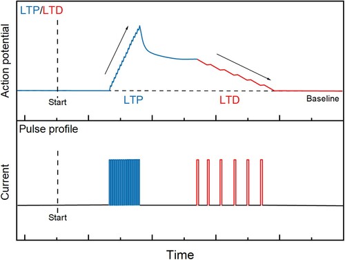
Based on the schematic diagram shown in Figure , the application of intense stimuli can be regarded as a training process for a neuron and LTP reflects the result of ‘learning’. Once the LTP occurs, the neuron may be boosted to a higher action potential by consecutively inputting an identical stimulus closely. LTD, on the other hand, could make the action potential depressed to the normal baseline, as the red curve in Figure , which often reflects the result of ‘forgetting’ in the biological nervous system. Therefore, this is the way a biological neuron can learn from different stimulus histories and then modify itself accordingly.As mentioned earlier, plasticity in biological neurons can originate from the neuron itself (intrinsic plasticity) or varied input profiles (synaptic plasticity). However, for artificial neurons in a solid-state device, it is hard to dynamically modify themselves once the device has been fabricated, so the intrinsic plasticity is difficult to be realized. As a result, artificial neurons may mainly rely on synaptic plasticity, which usually refers to spike-timing-dependent plasticity (STDP) and originates from different stimulus profiles rather than the changes in device properties. Therefore, LTP and LTD can be realized once the STDP indeed exists in the device. The observation of LTP and LTD in artificial neural systems aroused wide attention, which promoted the study of STDP and soon made it become an explicit topic to characterize neural performance after treating different stimulus conditions such as stimulus frequency, pitch and duration [Citation2,Citation14]. In the next section, the focus will be on how an artificial neuron works, the differences between artificial and biological neurons and the strategies to improve the efficiency of neuromorphic computing.
3. Artificial neurons and synapses
3.1. Neural network models
Although modern computing technology with super-fast computing speed attempts to compete with human brains in many aspects to help deal with data processing and information transfer, the human brain is still in the upper hand today. Therefore, we need to consider how to convert speed advantages to compensate for drawbacks of other aspects. Hopfield et al. proposed one of the pioneering approaches to mimic neural behaviour using electronic circuits [Citation15]. This approach consisting of N interacting neurons, expressed by non-linear differential equations, attempts to describe the states of neurons, which change with time due to the interaction among neurons and synaptic currents. Although the approach can fulfil the synaptic dynamics in a network and has been used for years, it is computationally expensive upon increasing the number of neurons, because several non-linear differential equations are required. That promoted some simplified approaches to accelerate the computation. However, the simplicity constraints the neuro-dynamics in reality; therefore, significant efforts have been devoted to looking for new approaches to function as human brains.
An ANN is a general framework, which transforms the inputs from pre-neurons to post-neurons through an activation function featuring a non-linear response with adjustable weights. The weight is given as the strength of the interaction between the pre-neuron (input, stimulus) and post-neuron (output). The goal of ANN is to approximate the input and make the output closer to the expected value. Each input, modified by its weight, is summed up and compared with the results in the database. The mismatch from the comparison will further adjust the weight to produce expected output. In general, utilizing a non-linear function may allow more flexibilities, while doing the approximation to fit the expected outcome, compared to utilizing a linear function. Therefore, conventional ANN introduces several kinds of non-linear functions, i.e. sigmoid, to adjust the weights to accomplish certain ANN tasks such as image recognition.
As described in Section 2, plasticity in biological neurons is an ability to adjust the amplitude of action potentials. In artificial neurons, plasticity is defined as the ability of how a neural network adjusts its weights. There are several types of ANN currently developed in terms of the way of adjusting the weight during signal processing.
Convolutional neural network (CNN) is one of the common neural networks used for image recognition. The process of CNN used for image recognition is described as follows: (1) The input image is cut into many segments. Depending on the complexity of the input data, the segments can be divided into many layers. For instance, colourful images can be divided into Red–Green–Blue layers. (2) A predefined matrix of weights is applied to all segments, namely a convolution process. After obtaining results from weight adjustments, the results are collected and computed by a specific non-linear function. It should be noticed that the background signal would be screened through a threshold of the non-linear process so the signature signal could be further processed for image recognition. (3) Thereafter, these final elements, which are the most representative signature for each segment, are compared with the trained database. Consequently, segments from the input image can be recognized by matching elements in the trained database. As a result, the non-linear function applied in CNN is the core of the image recognition task.
A recurrent neural network (RNN) is another type of ANN, which introduces a recurrent connection from the output back to the input. The additional feedback is designed for faster predictions. For instance, the feedback from the first approximation is applied as a new input for the next iteration, supporting the precise weight adjustment for the following computation. The recurrent connection makes RNN more temporally efficient since it helps to avoid unnecessary computation.
Unlike previous neural networks, a spiking neural network (SNN) does not use analog input/output. Instead, it utilizes time-dependent binary spikes as input/output. As introduced in Section 2, biological neurons transmit information through binary signals as the action potential. Also, they modify the signal through STDP. Computation in SNNs is similar to that in biological neurons, which utilizes time-dependent spikes to complete tasks. The plasticity in biological neurons can be induced by varying stimulus frequencies. The initial input spike is integrated and accumulated with the following input spikes within a period, resulting in a stronger response. In SNN, a leaky-integrate-fire (LIF) model has been proposed to mimic the time-dependent plasticity observed in biological neurons [Citation16]. The integration of spikes needs to be completed in a short time range; otherwise, it leaks over time with decreased strength; therefore, higher input-spike frequency results in stronger output, which provides a way for SNN to adjust its weights. Utilizing binary devices, SNN can achieve complex computation tasks using a spatio-temporal scheme, which makes SNN more energetically efficient due to the event-based functionality.
3.2. Differences between artificial and biological neurons
Biological neurons work at millisecond timescale and accomplish difficult tasks with astonishing energy efficiency, compared to the state-of-the-art CMOS-based ANNs. Here we itemize the uniqueness of biological neurons from several perspectives:
A biological neuron possesses dual functionalities as an information processor and memory in the same unit. However, the von Neumann bottleneck commonly appears in the current ANN architectures, which is an intrinsic obstacle that hinders the process of ANN towards a neuron-like efficiency because the training of ANN generates tremendous data to be processed and stored back and forth between the processor and memory. This leads to significant latency and energy consumption.
When a biological neuron receives a stimulus, its activation is determined by if the action potential surpasses its threshold. In computer science, weight is an equivalent factor to the strength of the synaptic signal received from a pre-neuron. Normally, the weight of an artificial neuron in a solid-state device is set permanently once the device is fabricated. However, biological neurons possess plasticity so the strength of the synaptic signal can be modified by interneural communications. Therefore, ANN typically requires extra devices and complex circuits to function as a biological neuron to host plasticity and tailor the weight. This structural design makes ANN, especially for CNN and RNN, energetically unfavourable. Even the most energetically efficient SNN today cannot rival a human brain regarding energy consumption.
The working principle of decision-making of a neural system has long been a tough topic in biological research [Citation17–19]. Neurons can communicate internally and then decide how to act, but ANN requires a huge array and complex circuit designs for communication among artificial neurons, which is always full of technical issues. It relies on the breakthrough no matter the development of materials or circuit designs, which are still challenging …
3.3. New computing architectures
Even with assistance from the ANNs, the current computing technologies are still far behind the requirements on low power consumption with a high calculation speed. Therefore, engineers are currently exploring various materials and structures under the ANN frameworks, which attempt to mimic the functionality of brains to reduce latency and boost energy efficiency. To address the issues, non-volatile memory together with memristive properties is the key to developing the hardware device for neuromorphic computing, which offers potential solutions to fit the rising computation demands nowadays. Several important breakthroughs and approaches are listed below:
Non-von Neumann architectures: The emergence of non-von Neumann architectures has brought the human brain as a model to build brain-inspired architectures to perform computation efficiently together by removing the memory bottleneck of the current architectures. Figure (a) shows a conventional computer without mature non-volatile memories; the bottleneck is about the huge power waste and latency because the information needs to travel back and forth between memory and process units. The corresponding strategy is to integrate the memory and process unit in the same device (Figure (b)) to realize in-memory computing [Citation20]. To build up an in-memory architecture, non-volatile memories are required for fast enough to read/write speed. Demonstrations of resistive random-access memory (RRAM) [Citation21,Citation22] and phase-change random-access memory [Citation23,Citation24] have been proposed for operational in-memory computing architecture. In-memory computing constructed using spintronic devices, for example, STT-MRAM will be covered in Section 4. Breakthroughs on in-memory computing composed of non-volatile memories have been shown to promote the ANN learning speed because of the reduced information travelling in circuits [Citation8,Citation20,Citation25].
Memristor as a building block for brain-inspired technologies: A memristor, combining adjustable resistance state with non-volatility, can provide analog outputs instead of digital ones. Applications of memristors appear to enhance computing capability via different resistance states and simultaneously reduce power consumption due to their non-volatility [Citation26]. For neuromorphic computing, the weights can be reflected on the memristor, whose state can be modulated by different operating histories, i.e. frequent pulse or narrow pulse duration. Recently, a great effort has been devoted to studying how to mimic a neural network since the first memristor-based functional array was demonstrated, as conceptually depicted in Figure [Citation27,Citation28]. Using memristors as the basic units to mimic neurons and synaptic behaviour provides the possibility of engineering memristor-based neural networks through circuit designs. Unlike conventional binary systems, memristors yield non-linearity in nature, whose properties determine a threshold and produce an analog output for varying weights. The non-linear dynamics of memristors appeal to introduce more flexible models, which can enable the optimization of the learning process in ANNs.
Figure 3. Computing architectures. (a) Schematic diagram of von Neumann architecture. Information in memories needs to be fetched to processing units and then stored back. (b) Schematic diagram of brain-inspired computing as non-Von Neumann architecture. Memory and processing units are in the same device.
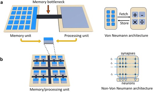
Figure 4. Neuromorphic computing architecture inspired by a human brain. (a) The brain computing architecture, built from the collection of neurons, is interconnected by synapses. (b) AI chips developed from brain-inspired architecture using memristors as artificial neurons interconnected in a crossbar array to mimic synaptic connections.
In addition to the two items above, quantum computing refers to the superposition and entanglement of states to develop algorithms, which are faster than conventional computing. In the past decade, superconducting qubits have demonstrated significant progress and their memory capabilities have been established, such as voltage-history dependence of the inductance and phase-dependent conductance [Citation29]. The quantum memristor, based on superconductive Josephson junctions [Citation30–32], serves as the building block for quantum neuromorphic computing [Citation33], and its integration with other quantum properties is expected to offer new functionalities, such as the entanglement of quantum memristors [Citation34], artificial synapses [Citation35], quantum neural networks on quantum processors [Citation36]. So far, the coherence times and the processing power of quantum processors have shown revolutionary breakthroughs in quantum-based neuromorphic computing. Controllable coherence in quantum neural networks could be beneficial to some extent such as non-linearity, making this approach more robust than the gate-based approach [Citation33]. Neuromorphic devices implementing quantum materials have also been realized, i.e. molecules and nanodiamonds [Citation37–40], taking advantage of the variable lifetime of their metastable states to provide intermediate states for short-term memory. Quantum materials offer unique features, especially in strongly correlated oxides, which possess a variety of macroscopic phases and enable the conversion of information modes by combining spin, charge and superconductive properties [Citation41].
4. Spintronics-based neuromorphic applications
4.1. Characteristics of MRAM
As one of the non-volatile memories, MRAM has been regarded as a promising candidate for in-memory neuromorphic computing since the architecture of magnetic tunnelling junctions (MTJs) was greatly improved in the last few decades [Citation42]. Composed of an oxide layer sandwiched by two magnetic layers in the form of a spin valve, the MTJ structure yields a large resistance change due to the tunnelling magnetoresistance (TMR) effect so the ‘1’ and ‘0’ bits can be well distinguished [Citation43]. Based on the concept of spin valves, one of the magnetic layers with lower coercivity (or without pinning) is defined as a free layer (FL) so it can be switched freely by external perturbation, i.e. magnetic field or spin current. Another magnetic layer, a pinned layer (PL) serving as a reference, often yields a larger coercivity or is magnetically pinned by an antiferromagnet. The switching of FL, which makes a parallel or anti-parallel configuration with PL, can give rise to a large resistance change of the MTJ (up to ∼500% at room temperature) [Citation44]. In addition to the natural non-volatility, which allows the low power consumption, current MRAM technologies also feature several unique characteristics for neuromorphic applications as follows:
Remarkable read-write speed. Switching is often at a nanosecond scale so the writing/reading can be done within a very short time [Citation45]. This would be a striking signature for MRAM compared with other memories.
Scalability. Reducing the writing current is one of the key developments of MRAM. In a practical sense, the amplitude of the writing current is proportional to the total magnetizations of FL so scaling MRAM down to a nanometer level is a straightforward strategy. The MTJ size is approximately 100 nm in diameter [Citation45,Citation46] or even 40 nm fabricated using advanced processing [Citation42].
Memristive property. The multi-level cell (MLC) has been reported in MRAM, which yields controllable resistance states together with non-volatility. So far, MLC in MRAM has been shown by manipulating the domain wall (DW) dynamics during the magnetization switching, especially in the case of SOT MRAM. It keeps promoting the potential of MRAM for possible neuromorphic applications in the future.
In addition to the mentioned advantages of MRAM, several kinds of properties in terms of different working principles were demonstrated to fulfil the different facets of ANNs. The developed MRAM and spintronics techniques including STT, voltage-controlled magnetic anisotropy (VCMA) and stochastic MRAM will be reviewed in this section. The developing MRAM technique currently based on SOT has been also demonstrated to be applicable for ANNs, especially on the issue of the spiking time-dependent plasticity (STDP). It provides space for external tuning on the device properties and will be reviewed in Section 5.
4.2. Spin-transfer torque MRAM and its applications
Predicted in 1996 [Citation47] and experimentally discovered in 1999 [Citation48,Citation49], the STT switching was the first current-driven magnetization switching for MRAM and soon became the major writing scheme in MRAM technology to the present. It was an encouraging discovery driving MRAM towards the whole electrical control withremarkable scalability, different from the traditional type of toggle magnetic field switching. This session will introduce STT from fundamentals to the current benchmark of in-memory computing arrays.
4.2.1. Working principle of STT
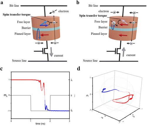
Figure is a schematic diagram to illustrate the STT switching mechanism in a spin valve (FL/barrier/PL) structure. When the electron current flows through the PL in Figure , the electron current can be spin-polarized to carry net spin flow in the device. Upon the itinerant spin interacting with the localized magnetic moment (as the FL layer in Figure ), it produces a torque to make a magnetic moment of the FL process. Therefore, the electron current penetrating the MTJ would attempt to switch the magnetization of FL once the amplitude reaches the threshold. By applying a current from FL (PL) to PL (FL) (as shown in Figure (a, b)), the parallel (anti-parallel) magnetization configuration of the final state can be achieved via the transmitted (back-reflected) spins from PL, so 0 and 1 can be easily defined by the low (parallel) and high (anti-parallel) resistance state across the MTJ. Figure (c, d)) shows the simulated STT-driven magnetization switching versus time and the spatial switching trajectory, respectively. Present STT-MRAM is structurally based on a two-terminal design, which shows great scalability and makes STT-MRAM ideal to be integrated with modern CMOS and even embedded cache memory [Citation50–52].
Figure 5. Writing mechanism of typical STT. (a) Writing a parallel magnetization configuration, in which the current is applied from FL to PL. (b) Writing an anti-parallel magnetization configuration, in which the current is applied from PL to FL. (c) Simulated STT-driven magnetization dynamics in a free layer versus time. (d) Magnetization trajectory corresponding to (c) in space.
4.2.2. Uniqueness of STT-MRAM
Since STT-MRAM is CMOS-compatible, a memory array of STT-MRAM has already revealed several neuromorphic demonstrations on STDP [Citation53]. While the spin-polarized current flows into MTJ cells, if the input current is insufficient, the output should be zero because of no magnetization switching. When the current exceeds the threshold, the magnetization of FL can be switched; however, writing errors may also occur in some situations, which may result from either magnetic uniformity due to fabrication or the back-hoping effect [Citation54]. Such writing errors become an issue in STT-MRAM so typically additional circuits may be required to avoid or correct writing errors. Interestingly, if a statistical analysis of writing errors can be summarized after performing writing tests, a non-linear correlation between switching probability and writing current can be often obtained. As discussed in Section 3, this non-linear curve, such as a sigmoid, could be applied for error correction. For instance, if a magnitude of writing current was expected to switch the magnetization but ultimately failed, it would be counted as one writing error. After summarizing all writing errors as a feedback report, the input magnitude could be self-calibrated to guarantee successful writing afterwards. Based on this idea, A. Vincent et al. demonstrated a simulated switching in an STT-MRAM array in 2015 [Citation55]. They first adopted the data from other STT-MRAM experiments [Citation56], then utilized the varied thresholds of writing current and recorded the time required for a complete switching. Typically, a larger writing current would lead to faster switching and higher switching probability. This work reported that switching probability versus delay time of complete switching could be fitted by a gamma distribution. As a result, their findings could provide a solid statistical prediction for switching probability as soon as the writing current is input to the MTJ cell. The work thus proposed a model to predict the smallest input current of STT-MRAM required for a complete switching.
Interestingly, their following work practically applied this self-calibrated approach to recognize cars on a highway [Citation53]. An array of STT-MRAM, composed of 32,678 MTJ cells, was applied for image recognition by assigning each MTJ cell as a pixel of an image. The final picture could be presented by MTJ output in the array. Electrical signals of pixels, originally from the camera, now are presented by 1 (white dots) or 0 (black dots). In the beginning, the reconstructed pictures for recognizing the moving cars were not clear because the individual STT-MRAM pixel cell showed writing errors. To improve the distinguishability of the pictures, they adopted the correlation of switching probability versus delay time for complete switching, claimed as a simplified STDP rule, to ‘train’ the STT-MRAM array to proceed with the self-calibration. Training is often an approach by applying an external stimulus to the investigated system, for example, the self-calibration of input to fix the writing error in this work. Before training, the image was extremely blurred because of considerable writing errors so the white pixel might turn out to be black. However, after signals were input five times in a row, the switched pixels would become stable, indicating that the MTJ array is ‘learning’ from the series of inputs. Note that learning is often a process to make a system respond to the input stimulus properly, which typically needs to be assisted by an algorithm. Therefore, learning in this study reflects on the stabilization process of the switched pixels in the MTJ array. After the learning, each pixel could yield a nearly correct value and a quite recognizable image was presented. Although writing errors might occur in an array of STT-MRAM, they could be gradually improved using multiple inputs and specific artificial STDP learning rules.
Zheng et al. proposed using the STT-MRAM as the building blocks for the artificial RNN learning design [Citation57]. As reviewed in Section 3, artificial neurons in RNN have an additional recurrent mechanism to have ‘feedback’ and then self-correct the original information correspondingly. In this work, the inputs for the STT-MRAM array composed of 40 cells are not conventional writing pulses, but AC in the form of a sine wave. Unlike a pulse signal, an AC input would oscillate the magnetic moment in FL, so the output signal would be also a sine wave. In this work, they input a continuous AC of a sine wave as training inputs. A force-learning algorithm [Citation58] was also applied to the learning process. At first, consolidation output from the STT-MRAM array does not perfectly match the input sine wave. Each STT-MRAM might have slight variations in its oscillation frequency or magnitude. After the AC input for 3000 ns, collective output signals are stable and perfectly match the input magnitude. Afterwards, as soon as they change the input profile of the sine wave, 40 STT-MRAMs took another 3000 ns to match themselves to the input signal.
For the typical set-up of RNN, additional circuit designs are required for the correction. In Zheng’s work, although the feedback takes a period to stabilize the oscillation from FL, which could be regarded as a ‘training’ process, this design did not require any additional recurrent circuits, thus simplifying the whole structure for computing. The stabilization process after changing input is equivalent to the correction circuits in RNN. The CMOS-based RNN circuits are often complicated, but this work demonstrated how to use only 40 STT-MRAMs to substantially simplify the circuit required to realize RNN functionality, making this work solid proof that STT-MRAM is capable for advanced neural networks [Citation57].
4.2.3. Stochastic MRAM
Traditional memory provides digital information, which would possess an energy barrier larger than 60 between ‘1’ and ‘0’ states to ensure acceptable thermal stability. On the other hand, the recently developed quantum computing gives a new concept for computer science. Unlike traditional computers, which use digital bits, the quantum computer could have a superposition state within a single bit, the so-called qubit. The qubit could make neural networks work more efficiently since it provides multiple possibilities instead of predictable results. Recently, a stochastic magnetic tunnelling junction (SMTJ) has been developed to exploit magnetization with weak thermal stability [Citation59]. The energy barrier of SMTJs should be lower than 15 so the magnetizations of FL can freely hop between the anti-parallel (AP) and parallel (P) states (Figure (a)) after giving a writing input; therefore, the magnetization switching may not be precisely predicted and controlled due to thermal fluctuation. SMTJ can be used as a probabilistic bit (p-bit), which naturally fluctuates between ‘0’ and ‘1’, and can be integrated into stochastic neural networks acting as a binary stochastic neuron, as shown in Figure (a), namely whose switching property cannot be predicted.
Figure 6. Experimental demonstration of a p-bit. (a) Electrical diagram of a p-bit consisting of an SMTJ, an NMOS transistor, a comparator and a resistor. (b) Time-averaged as a function of applied input
, fitted to sigmoidal function. (c) Time snapshots of
for three inputs
, showing a preferred state of the p-bit (high or low) as a function of its input voltage. Copyright 2019, Springer Nature [Citation59].
![Figure 6. Experimental demonstration of a p-bit. (a) Electrical diagram of a p-bit consisting of an SMTJ, an NMOS transistor, a comparator and a resistor. (b) Time-averaged VOUT as a function of applied input VIN, fitted to sigmoidal function. (c) Time snapshots of VOUT for three inputs VIN, showing a preferred state of the p-bit (high or low) as a function of its input voltage. Copyright 2019, Springer Nature [Citation59].](/cms/asset/cecf9f06-3e38-4d24-9149-75254a5f76a8/tmrl_a_2147803_f0006_oc.jpg)
The demonstration of p-bit adopts the idea of quantum computing but with more accessible hardware devices. The key challenges lie in how to introduce stochasticity in SMTJ while maintaining its controllability for writing ‘0’ and ‘1’. In an ideal MTJ with high thermal stability, the writing current over a critical threshold would switch magnetization between two distinguishable resistance states. On the other hand, in an SMTJ, the low magnetization retention originating from low anisotropy (right-hand side of Figure (a)) would yield significant stochasticity because the low anisotropy cannot effectively confine the magnetization at the P/AP state. This stochasticity tuning via controlling anisotropy strength can be directly done by reducing the volume of the FL with decreased diameter or thickness. As shown in Figure (b), the magnetization state can be read out across the SMTJ after averaging the Vout signal during the retention (∼100 ms) (Figure (c)). The Vout signal is a function of the writing voltage Vin, in which a larger (smaller) Vin would favour the AP (P) state so the Vout–Vin correlation would appear like a sigmoid response (Figure (b)). This property can be employed to mimic the activation function of ANNs and this study successfully demonstrates how to convert the stochasticity to control the magnetization state in a p-bit.
Kaiser et al. [Citation60] attempted to utilize low input current to achieve the expected output of SMTJs through specialized circuits and algorithms. In their work, the SMTJ-based full adder has the functionality of self-calibrated modification. The signal retention from SMTJ-based full adder is traced for approximately 100 ms after the input. The output is then compared to the one from the ‘ideal’ MTJ-based full adder with high thermal stability as a reference. Subsequently, the input current for writing SMTJ is modified according to its mismatch to the current required for writing an ideal MTJ. After a certain training and retention period, the output of an SMTJ-based full adder shows self-correction to the value as done by an ideal MTJ-based full adder. This result indicates that p-bit based on SMTJ may provide advantages of superposition as ones in qubits after being arranged in the algorithm of a full adder.
Adopting the same idea, a neural network can be built by the interconnection of SMTJs. The input for each SMTJ comes from two outputs of other SMTJs, and the weights are updated based on the SMTJ with a lower energy barrier within one writing event. Pervaiz et al. interconnected 8 p-bits to build an 8-bit asynchronous p-computer [Citation61], which can solve optimization problems and integer factorization, tasks generally assigned to test quantum computing algorithms [Citation59]. The artificial synapse was built using a microcontroller that converted the digital output from other SMTJs to an analog input for another SMTJ. The convergence of the learning process was determined by the synapse time, defined by the microcontroller, often in the order of 100 to 1 ms. It needed to be smaller than the SMTJ’s retention time, which was in the order of 10–100 ms. The successful training was often time-consuming because it took approximately 1000 s, in general, to wait for the output stabilization in SMTJs [Citation60]. The increase of learning speed can be achieved by changing the circuit design to a crossbar architecture where the synapses can operate with GHz speeds with the execution time down to 10 ps and the fluctuation time of SMTJs can be in the order of 100 ps. Stochastic computing or p-computing has gained interest to serve as a partial bridge between spintronics and quantum computing and to perform specific quantum computing applications without the expensive hardware constraints used for quantum bits. Additionally, stochastic neural networks represent a natural alternative to mimic the stochastic process that occurs in the brain.
The last example of STT-MRAM for neuromorphic computing is the realization of in-memory computing, reported by a Samsung Electronics group [Citation8]. The development of modern computer technology is stuck by transition delay between processing units and memory, so one of the practical solutions is to realize in-memory computing. If the CPU can integrate memory inside itself, the delay between read/write and storage devices would be avoided; therefore, crossbar-type in-memory computing was developed correspondingly to address the delay [Citation20]. In Samsung Electronics’ work [Citation8], the demonstration of an in-memory chip is composed of 6464 STT-MTJ crossbar arrays. Each bit-cell consists of two transistors and two MTJs in the form of 2T2M for basic logic calculation. This 2T2M architecture could perform the functionality of an XNOR gate. They demonstrated that the chip could do image recognition by itself, which became the most intriguing point of this work.
4.2.4. Voltage control magnetic anisotropy and its applications
Magnetization can be switched by electricand magnetic fields via the magneto-electrical interaction. Based on this concept, not only the magnetization but also the anisotropy can be changed using an electrical field. It is the principle of voltage-controlled magnetic anisotropy (VCMA) [Citation62]. VCMA has attracted attention for neuromorphic applications since the observation in 2011 by Wang et al. [Citation63]. Although applying an electrical field alone could not drive a deterministic magnetization switching in the regular MTJ design, it indeed influenced the switching current and the property of stochastic switching. Several neuromorphic applications based on VCMA-MRAM have been demonstrated:
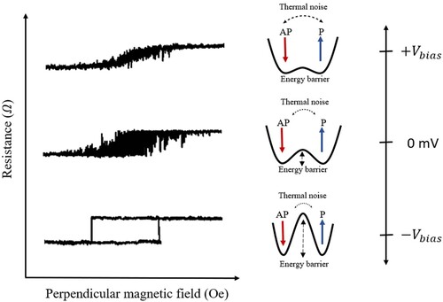
Cai et al. presented the first VCMA in a single MRAM cell [Citation64], in which the magnetic switching through different applied voltages across the MTJ cell could be observed. The MTJ cell containing an ultra-soft FL yielded different field-to-resistance curves while applying an electrical voltage and magnetic field simultaneously. In this demonstration, field-assisted magnetization switching was conducted first, which looked like normal MTJ behaviour. However, applying a strong electrical field on the MTJ cell would lead to stochastic switching because of the reduction in coercivity and anisotropy field. In an ideal MTJ, switching in FL should always take place around the coercivity. However, under an external voltage as a fluctuation, the magnetization of FL can freely switch between AP/P states because of the reduced anisotropy confinement, and thus the expected deterministic switching vanishes accordingly, as shown in Figure . When experiencing an identical field sweeping, the MTJ cells with a voltage applied would show stochastic switching near the zero fields. The stochastic behaviour is similar to what has been observed in STT-MRAM. It enables similar stochastic applications as introduced in SMTJ. Consequently, this stochastic property ensures the potential of VCMA to be applied for image recognition.
Figure 7. Schematic diagram to illustrate VCMA effect on the modification of switching barrier (at right) and its associated switching properties on the magnetoresistance measurement (at left).
To further introduce plasticity, Mishra et al. used a gate voltage to drive oxygen migration adjacent to the gate to mimic synaptic behaviour [Citation65]. Figure (a–d) shows the experimental details of this work, including the material and the device structure. Due to the gradual propagation of oxygen ions within the resistance layer (GdOI) (Figure (a–b)), the whole structure could behave in a typical learning/forgetting curve, similar to biological synapses. When applying a strong enough stimulus, i.e. a positive gate voltage on the light blue area of the device (Figure (c)), anomalous-hall effect (AHE) resistance (RAHE) of the device started to increase until the relief of voltage, as shown in Figure (d) and then the AHE signal started to decrease if no voltage was applied on the device. Because the migration of oxygen would significantly influence the magnetic anisotropy of Co due to the different degrees of Co oxidation, leading to the varied RAHE signals, shown in Figure (d). The decay of the RAHE signal in Figure (e) coincides with the customized Kohlrausch equation referring to ‘forgetting’ in a human brain [Citation66]. Ultimately, they also proposed that an MRAM cell could perform a typical response as LTP.
Figure 8. Demonstration of learning and forgetting curve in the structure of Pt/Co/GdOx. (a) and (b) The oxygen ions (blue dots) diffuse along the direction of an external electrical field. (c) Optical microscope image for the device geometry. (d) Applying a certain voltage on the device would result in an increase in AHE resistance. After releasing the voltage, the AHE signal started to decay. (e) Potentiation fitting for both device (dots) and model from nature (solid line). Copyright 2019, American Physical Society [Citation65].
![Figure 8. Demonstration of learning and forgetting curve in the structure of Pt/Co/GdOx. (a) and (b) The oxygen ions (blue dots) diffuse along the direction of an external electrical field. (c) Optical microscope image for the device geometry. (d) Applying a certain voltage on the device would result in an increase in AHE resistance. After releasing the voltage, the AHE signal started to decay. (e) Potentiation fitting for both device (dots) and model from nature (solid line). Copyright 2019, American Physical Society [Citation65].](/cms/asset/f26e0ca1-ef13-46da-bdbd-270ea9d78eaf/tmrl_a_2147803_f0008_oc.jpg)
5. SOT-based neuromorphic applications
5.1. Introduction of SOT switching and SOT-induced multi-levels
Miron et al. demonstrated a current-induced magnetization switching in a heavy metal (HM)/ferromagnet (FM) bilayer Pt/Co with a perpendicular anisotropy [Citation67]. As conceptually depicted in Figure (a), while a horizontal charge current flows into the HM layer, a vertically diffusing spin current is generated by the spin Hall effect [Citation68–70], which leads to opposite spin accumulations at the top and bottom surface of HM (Pt). Consequently, the spin accumulation in the vicinity of the HM/FM interface would induce a torque to re-orientate FM (Co) magnetization via two kinds of effective field induced by field-like torque along the y-direction and damping-like torque along the x-direction [Citation71,Citation72], as shown in Figure (a). During the application of current-induced torque, an external field collinear to the applied current is required to break the reversal symmetry of the magnetization, leading to deterministic switching [Citation70,Citation73]. It is the core concept of writing in the 3rd MRAM generation, which uses the spin current generated in HM to switch the adjacent FM. Because the spin torque is generated mainly by the spin Hall effect as a result of strong spin-orbital coupling in HM, the torque is named SOT afterwards [Citation74,Citation75].
Figure 9. SOT-driven magnetization switching in HM/FM heterostructures. (a) Spin current injection from heavy metal (HM) and generation of spin accumulation at the top and bottom surfaces of HM. (b) DMI effect at heavy metal/ferromagnet (FM) interface leading to the neighbouring spin canting. (c) Magnetization switching by SOT-driven DW propagation. (d) Magnetization switching by SOT-driven nucleation of reversed domains.
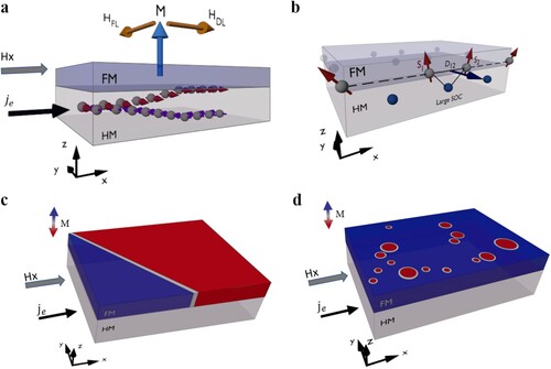
The magnetization switching by SOT was related to the DW dynamics and could be affected by the Dzyaloshinskii–Moriya interaction (DMI) naturally developed at the HM/FM interface (Figure (b)) [Citation76,Citation77]. The DMI is a peculiar interaction that generates a canting angle between the neighbouring spins at the HM/FM interface and determines the speed of DW motion during magnetization reversal [Citation78–80]. In addition to the dynamic issue, the different DW types were also associated with the strength of DMI. For example, in the perpendicular magnetization system, the strong DMI would result in a Néel type DW with a specific chirality [Citation81,Citation82]. In addition, the nucleation of reversed domains and subsequent DW propagation could be observed during the SOT switching (Figure (c)). Instead, once the DMI strength is too small to sustain the Néel type DW, a mixed DW type between Néel and Bloch DW may exist [Citation83,Citation84]. In this situation, nucleation-driven switching can be observed, as depicted in Figure (d). The precise control over the domain dynamics has been currently appealing in this field because the MLC could be observed once the magnetic intermediate states could be finely controlled via a gradual DW propagation or nucleation of reversed domains.
Many approaches have been reported to exploit the interplay between SOT and DMI for generating an MLC because this property can artificially mimic the synaptic weight. Under an external stimulus, action potentials from the pre-neuron are transmitted through the synapse to the post-neuron, together with varied synaptic weight. Huang et al. reported the generation/stabilization of MLC using Co/Pt multilayers [Citation85], turning the typical binary switching to an analog switching with robust MLC. The impact of this work is that the MLC could be achieved without the initialization, that is, the intermediate states can be directly achieved without initialization to the saturation state, which was typically required in most of the MLCs. The output of MLC was simply determined as a function of current amplitude and polarity [Citation86].
Fukami et al. demonstrated a field-free SOT device with the feature of MLC in a PtMn/(Co/Ni) system, in which Co/Ni multilayer could host the perpendicular anisotropy and antiferromagnetic (AFM) PtMn could establish an in-plane exchange bias collinearly aligned with the input current [Citation87]. In this study, the dual functionalities of PtMn generating spin current and in-plane exchange bias enabled field-free SOT switching because the existence of in-plane exchange bias could serve as an in-plane effective field to break the SOT reversal symmetry of Co/Ni. Besides, because of the varied coupling strength between FM and AFM (PtMn) among grains at the interface and the different alignment of exchange bias direction with the applied current, the gradual domain reversal accompanied by increasing the writing current produces the MLC at the zero fields. This work aroused attention to using AFMs to be the spin current source and a pinning layer to realize field-free MLC by SOT. Huang et al. further demonstrated an MLC with a ratchet effect as a result of the exchange spring coupling in an IrMn/perpendicular CoFeB bilayer, in which the SOT switching following (against) the exchange bias would feature an analog (digital) property [Citation88]. This digital–analog duality is first observed in a single SOT device with AFM. This observation also promoted the AFM materials to be more active in the MRAM-related research field. Interestingly, it has been shown the spin current does not only switch the FM magnetization but also reverses the direction of exchange bias in an HM/FM/AFM trilayer system [Citation89], which may realize the thermally stable SOT device at the nanoscale because exchange bias can be switched during SOT pulse on but is fixed afterwards.
5.2. Current achievements of neuromorphic computing applications using SOT
The achievement of MLC in SOT-MRAM opens a new avenue towards neuromorphic applications because the precise control of multi-level switching enables a cell to produce an analog response. Since the MLCs were demonstrated in multilayers [Citation85,Citation90], heterostructures [Citation91–93] and in an AFM/FM exchange-coupled system [Citation87,Citation89,Citation94], manipulating the domain and DW dynamics to accommodate intermediate states in a SOT device has been proposed through different manners [Citation95–98]. To mimic the neuron property using SOT devices, some artificial stimulations have been used to activate neuromorphic responses in SOT devices and further explore the plasticity.
Liu et al. demonstrated neuromorphic LTP and LTD in ferrimagnet-based (CoGd) SOT devices by varying the current pulse polarity [Citation95]. That is, consecutively applying a positive (negative) current pulse leads to the LTP (LTD) on the output electrical signal. They demonstrated how LTP (LTD) is achieved by the observation of magnetic domains. The gradual increment (decrement) of current pulses will nucleate new reversed domains with limited propagation, allowing the analog-like output and preserving the magnetic states due to the non-volatility. The variations of the magnetic states, read out by anomalous hall resistance (RH), on SOT switching can be used for representing synaptic weight. Based on the LTP and LTD, this ferrimagnetic artificial neuron can be used to recognize a handwritten digit performed by simulated multilayer perceptron (MLP), and the recognition accuracy is approximately 93%.
Zhou et al. reported the domain nucleation-dominated SOT switching in an L11-CuPt/CoPt bilayer, giving rise to an MLC property as a sigmoidal neuron for a deep learning network [Citation96]. Live training based on these spintronic neurons achieves a high recognition rate on the handwritten digit recognition, comparable to the results of pure simulation based on an ideal sigmoid function. Additionally, the L11-CuPt/CoPt bilayer provides field-free switching due to a SOT symmetry-breaking, originating from its low-symmetry point group (3 m1) [Citation99]. This structure simplifies the layer design, and its switching by nucleation makes it less rigorous against defects than in the case of propagation.
Cao et al. reported the field-free STDP in an interlayer exchange-coupled SOT device (Pt/Co(perpendicular magnetization)/Ta/Co (in-plane magnetization)), which was treated as an artificial synapse to joint pre-neuron and post-neuron, as shown in Figure (a) [Citation97]. Due to the presence of in-plane Co, the multi-level SOT switching of perpendicular Co can be realized without the assistance of an external field. Under the STDP process, if a neuron receives an input spike immediately before, or after, it outputs a spike, the input may make the output stronger or weaker. This work demonstrated that the artificial synaptic plasticity reflected by RH could be modulated by the temporal gap (causality, ) of the spikes, defined by the time difference on inputs from both ends in the current channel of the device (input along the
x-direction in Figure (b)), in which the pre-spike and post-spike shared the same waveform but were opposite in polarity. Although a single pre- or post-spike did not exceed the threshold current, the overlapped waveform will produce a short peak over the threshold, of which sign and magnitude depended on the Δt. A LTD or LTP of the synaptic weight occurs when the post-neuron spikes just before (Δt < 0) or after (Δt > 0) the pre-neuron spikes, respectively, as demonstrated in Figure (c). The |Δt| dependence of the synaptic potentiation/depression magnitudes is similar to that of the biological synapse, i.e. closer spikes bring a stronger stimulus. A biological synapse realizes such plastic functions by regulating the ion concentrations, as discussed in Section 2. Although there is still a lack of explanation on the RH-
correlation in this study, the results suggest that giving the stimuli with changes in the time domain would indeed influence the output of the device, reflecting the existence of plasticity for the adjustable weight of ANNs.
Figure 10. SOT-induced STDP in the artificial synapse. (a) Scheme of synapse between a pre-neuron and post-neuron. (b) Artificial synapses modulated by the causality of the spikes from both ends of the x channel. (c) STDP window with the spikes shown in (b). Copyright 2019, Wiley [Citation97].
![Figure 10. SOT-induced STDP in the artificial synapse. (a) Scheme of synapse between a pre-neuron and post-neuron. (b) Artificial synapses modulated by the causality Δt of the spikes from both ends of the x channel. (c) STDP window with the spikes shown in (b). Copyright 2019, Wiley [Citation97].](/cms/asset/4795d15d-434e-4542-bfc6-7cb507217efb/tmrl_a_2147803_f0010_oc.jpg)
Kurenkov et al utilized AFM/FM SOT devices to demonstrate the functionality of both neurons and synapses on the same material system by changing the device size [Citation98]. This work simultaneously utilized temperature dynamics, SOT switching dynamics and the unique device size-dependent behaviour of AFM/FM heterostructures. This AFM (PtMn)/FM (Co/Ni) stack was patterned into 100 nm devices with binary switching for neurons and 5 µm analog devices for synapses (Figure (a)). The weight function of the 5 µm analog device is electrically equivalent to the spike-timing-dependent update of a biological synapse, as shown in Figure (b). On the other hand, for the 100 nm device with binary switching, the two magnetization states were associated with a non-firing and firing states of a neuron and the temperature represented the excitation level. The observed dependencies of firing probability on the frequency (Psw vs. fin) (Figure (c)) and number (Psw vs. npulses) (Figure (d)) of incoming stimuli reproduce LIF functionality of a biological spiking neuron.
Figure 11. Synaptic and neuronal functionalities and their realizations in AFM/FM heterostructures. (a) Scheme of the device structure. Left inset: 5 µm artificial synapse with analog output. Right inset: 100 nm artificial neuron with binary output. (b) Weight update function of the artificial synapse, composed of a 5 µm analog device, produced by pairs of rectangular pulses with delays Δτ from −5 to 5 µs. (b) Dependence of switching probability on the frequency
of incoming trains of
pulses for an artificial neuron, composed of a 100 nm binary device. (c) Dependence of
on
for an artificial neuro with
fixed at 8 MHz. Copyright 2019, Wiley [Citation98].
![Figure 11. Synaptic and neuronal functionalities and their realizations in AFM/FM heterostructures. (a) Scheme of the device structure. Left inset: 5 µm artificial synapse with analog output. Right inset: 100 nm artificial neuron with binary output. (b) Weight update function of the artificial synapse, composed of a 5 µm analog device, produced by pairs of rectangular pulses with delays Δτ from −5 to 5 µs. (b) Dependence of switching probability Psw on the frequency fin of incoming trains of 104 pulses for an artificial neuron, composed of a 100 nm binary device. (c) Dependence of Psw on npulses for an artificial neuro with fin fixed at 8 MHz. Copyright 2019, Wiley [Citation98].](/cms/asset/e7732bdf-4320-419e-9860-079be4ae3d46/tmrl_a_2147803_f0011_oc.jpg)
5.3. Spin Hall nano-oscillators for neuromorphic applications
The integration of artificial neurons into large-scale ANN represents a great engineering challenge. For complex tasks, the ANN must consist of several layers of interacting artificial neurons to achieve accurate predictions. STT-nano-oscillator (STNO) [Citation100] was proposed to address this issue; Later, Zahedinejad et al. [Citation101] using a similar idea but a simplified process demonstrated a spin Hall nano-oscillators (SHNO) to address the same issue STNO encountered. Based on the architecture of SOT devices, SHNO in the form of a three-terminal structure utilizes pure spin current from the HM layer to excite the adjacent magnetization and then achieve steady-state precession, which emits a microwave with a specific frequency. The fabrication of nano-constrictions in the magnetic layer can be used as individual artificial neurons [Citation102], which are capable of mutual synchronization with their neighbouring neurons by magnetic exchange and dipolar interactions. Large-scale implementation of SHNO has been demonstrated in 2D arrays and the individual frequency tuning is achieved by modifications of the dimensions of nano-constrictions [Citation101]. SHNO can perform tasks such as voice recognition by mapping synchronization ranges for each vowel, with low operation power and large mutual synchronization. However, the frequencies are set when the devices are fabricated; therefore, this approach did not allow frequency adjustment for weights to train the ANN for neuromorphic applications due to the lack of plasticity.
To overcome this issue, a promising alternative to control individual artificial neurons was proposed by Zahedinejad et al.[Citation103]. The integration of an oxide gate with SHNO, as shown in Figure (a–b), provides manipulation of auto-oscillation frequency by adjusting the magnetic anisotropy, leading to large-scale mutual synchronization. When an electric field is applied to the gate oxide, conductive ionic filaments would be formed accompanied by migration of oxygen anions and metal cations, as shown in Figure (b). These ionic filaments would remain even after turning off gate voltage later, and hence preserved the non-volatility in each SHNO. The ionic motion intrinsically alters the magnetic anisotropy, and thus changes auto-oscillation frequency. Furthermore, the variations on ionic filament density controlled by gate voltage lead to a memristive response of the microwave output, serving as an ideal candidate for ANN thanks to the control of the mutual synchronization used as weights.
Figure 12. Schematic diagram of SHNO with a memristive gate fabricated on the top of the nano-constrictions. Operating in (a) HRS and (b) LRS. (c) MLC switching of the memristive gate. (d) SHNO chain consisting of seven nano-constrictions connected by six bridges. (e) AO frequency versus nano-constriction number when no additional current is provided by the gates. (f) AO frequency of the same SHNO chain when each gate voltage matches its programmed resistance such that the frequency of each nano-constriction reaches that of its upstream neighbour. As a consequence, all SHNOs mutually synchronize on the frequency of the first SHNO. (g) AO frequency of the same chain when two of the input voltages do not match their programmed resistances (indicated by grey arrows). Here, is too low, and
is too high and as a consequence, the chain is only partially synchronized as it breaks up into three different segments (cuts indicated by blue dashed lines). Copyright 2022, Springer Nature [Citation103].
![Figure 12. Schematic diagram of SHNO with a memristive gate fabricated on the top of the nano-constrictions. Operating in (a) HRS and (b) LRS. (c) MLC switching of the memristive gate. (d) SHNO chain consisting of seven nano-constrictions connected by six bridges. (e) AO frequency versus nano-constriction number when no additional current is provided by the gates. (f) AO frequency of the same SHNO chain when each gate voltage matches its programmed resistance such that the frequency of each nano-constriction reaches that of its upstream neighbour. As a consequence, all SHNOs mutually synchronize on the frequency of the first SHNO. (g) AO frequency of the same chain when two of the input voltages do not match their programmed resistances (indicated by grey arrows). Here, V2 is too low, and V5 is too high and as a consequence, the chain is only partially synchronized as it breaks up into three different segments (cuts indicated by blue dashed lines). Copyright 2022, Springer Nature [Citation103].](/cms/asset/09076237-4fdd-4330-9ae5-112cd48aae54/tmrl_a_2147803_f0012_oc.jpg)
This approach quantitatively improved the performance relative to their previous work, in which only partial devices could be synchronized due to the differences in the structural constrictions [Citation104]. When the system is in the high resistance state (HRS), as shown in Figure (a), no conductive paths are formed in the insulating layer, and only the electric field alters magnetic anisotropy, thus changing the precession angle of the magnetization. On the counterpart, when the system is driven to the low resistance state (LRS) (Figure (b)), the resistance state can be further changed by sweeping the gate voltage under current compliance (CC) to manipulate the size of the conducting path in the insulating layer, leading to memristor behaviour, as shown in Figure (c). Figure (d–e) shows 7 SHNO with individual auto-oscillating (AO) frequency due to different sizes of the constrictions. To drive the oscillator network into synchronization, the gate voltage must match the programmed resistance, and hence mutual synchronization is achieved, as shown in Figure (f). Figure (g) shows the case when two gate voltages do not match the programmed resistance so the mutual synchronization breaks and three synchronized segments are formed. SHNOs with memristive functionalities are attractive for new computing architectures aiming to eliminate the von-Neumann bottleneck since the weight adjustments for individual SHNOs allow the training in oscillator networks.
5.4. Skyrmion-based SOT device for neuromorphic applications
Magnetic skyrmions, first theorized by Skyrme in 1962 [Citation105], are one kind of quasi-particles with a specific spin texture at the nanoscale. Extensive research studies have been conducted to fabricate skyrmion-based memory and logic applications because of the low current density required to drive skyrmion nucleation and propagation in magnetic multilayers. Büttner et al. reported the SOT-driven generation and motion of skyrmions for the racetrack memories [Citation106]. The stabilization of magnetic skyrmions at room temperature has been a challenge for long [Citation107]. The significant large DMI found in magnetic multilayers such as Co/Pt multilayer provides the required energy to stabilize skyrmions at room temperature; therefore, the nucleation and propagation of skyrmions using magnetic multilayers have been studied for novel computing applications [Citation108,Citation109]. Once nucleated, skyrmions show quasi-particle-like behaviour and can be transported by external forces like a magnetic field or current. Incorporating imperfection sites in the device assisted in creating skyrmions by SOT due to the reduced perpendicular anisotropy [Citation106,Citation110].
SOT provides skyrmions with an additional force to change skyrmions’ trajectories, depending on skyrmion size, defects along the motion path and the strength of SOT. The precise control over skyrmions’ position by SOT-driven motion is useful for neuromorphic applications [Citation111,Citation112]. Song et al. developed a skyrmion-based system as an artificial synapse by the accumulation/decrement of skyrmions. They showed how the change in the number of skyrmions in the sensing area can mimic the potentiation (LTP) and depression (LTD) of a synapse, which can be accomplished using consecutive positive (negative) current pulse, respectively [Citation113]. Then, they simulated an ANN for the pattern recognition with a skyrmion synapse device in a 2T1R configuration, showing the skyrmion-based ANN can achieve a training accuracy of ∼93%, comparable to the accuracy obtained using standard software. The approach shows a promising future for skyrmion-based computing technologies. However, a real demonstration of ANN using skyrmions is not demonstrated yet.
6. Challenges and outlook
Current developments in neural networks are fully based on brain-inspired technology; therefore, a large number of neurons and synapses need to work together to process the information and then make the decision, which brings serious issues of energy and latency in the neural network. Spintronics-based neuromorphic technology becomes an ideal candidate to potentially solve the energy and latency issue thanks to its intrinsic non-volatility and remarkable scalability, which distinguishes the spintronic device (including MRAM) itself from other devices or memories to be one of the dominant branches in neuromorphic computing. Although spintronic devices look promising to make neuromorphic computing more energetically efficient, there still exist several challenges to making spintronic devices one step away from the practical ANN.
Non-linear input-output response (non-linearity) is the basic requirement for ANN, i.e. Sigmoid in CNN. On the other hand, the conventional MRAM design only reveals its binary nature and allows digital output. Therefore, searching for a specific system featuring analog output as a memristor, as described in the previous sessions, is the way to work out for non-linearity. The emergent SOT techniques should be one of the important MRAM families to play a role in this perspective. It may be a great breakthrough to use a single SOT-MRAM cell as a memristor to replace a colossal array structure, simplify circuit design and perform the remarkable non-linear analog output through precise control over the DW dynamics. Utilizing an AFM [Citation98], inter-exchange-coupled FMs [Citation97] and even ferrimagnet [Citation95] has enabled the control over the DW dynamics to reveal memristive properties. Furthermore, magnetization switching driven by SOT would not influence the microstructure of devices and shows good reversibility to fundamentally address the reliability issue in real operation.
The next issue is associated with scaling because it indeed affects how ideal a memristor can perform, i.e. how many intermediate states of an MLC can be obtained when scaling down. This forces researchers to rethink if there is an effective strategy to incorporate more intermediate states with remarkable controllability and distinguishability in the MLC for analog output. The resistance changes based on MTJs are typically much smaller than the other emergent memory technologies, which makes robust intermediate states even more challenging. Precise control over the DW position during the switching, refining the reversed domains or reducing the skyrmions’ size can be possible solutions to address the issue. The introduction of AFM may incorporate more ingredients into present SOT-MRAM on many aspects such as MLC [Citation74], ratchet [Citation75] and thermal stability [Citation76], which may provide another tuning knob for robust intermediate states.
Non-volatility is the common advantage of MRAM, but it may be also an opposite pronoun of stochasticity. The implementation of SMTJ due to its stochasticity not only demonstrates a new kind of framework of neuromorphic computing but also bridges the beauty of quantum application using spintronics. On the other hand, ideal non-volatility often requires robust anisotropy to sustain the magnetization state, so it may not allow stochasticity [Citation114]. This issue would be also correlated with the memristive property, which needs sustainable intermediate states for memory. The balance between stochasticity and robust anisotropy to sustain non-volatility should be taken into account. Memristor with plasticity may be one of the possible solutions because the plasticity reflects on the changeable response of an MRAM cell as manipulating the external stimuli; therefore, plasticity may provide space to introduce stochasticity into the system.
To reduce the energy consumption at the device level, the electrical current threshold to drive magnetization switching should be further reduced. In addition to the conventional strategy with scaling, exploring new materials with a stronger charge-to-spin conversion effect is essential, which refers to the spin Hall angle of HMs [Citation69,Citation115]. This issue promotes the exploration of new metal alloys [Citation116–118] and the potential topological insulators [Citation119–121], of which the charge-to-spin conversion effect is larger than that of a typical HM. The recently reported topological Dirac semimetal can also be one of the potential solutions [Citation122]. Furthermore, different combinations of spintronic approaches, i.e. SOT+VCMA or SOT+STT [Citation123], may also reduce the writing current significantly.
The items reviewed above are all specific issues of using MRAM (or spintronic devices) for neuromorphic computing. The trade-off, among the properties above, leads to even more complicated challenges for developing spintronics-based neuromorphic computing. On the other hand, significant progress has been gradually realized by various proof-of-concept neuromorphic computing implementations with spintronic materials and devices, as demonstrated in Sections 4/5. With the further exploration of novel materials and circuit designs, a large-scale ANN based on spintronic devices will pave a new avenue for neuromorphic computing. To achieve this goal, technical issues may be potentially encountered in the large-size fabrication together with CMOS-compatible techniques. It implies that technical breakthrough is always the basis of developing a functional ANN architecture, which needs more effort to get involved from various fields.
Disclosure statement
No potential conflict of interest was reported by the author(s).
Additional information
Funding
References
- Bouzy B, Cazenave T. Computer Go: an AI oriented survey. Artif Intell. 2001;132(1):39–103.
- Tang J, Yuan F, Shen X, et al. Bridging biological and artificial neural networks with emerging neuromorphic devices: fundamentals, progress, and challenges. Adv Mater. 2019;31(49):e1902761.
- Schuman CD, Kulkarni SR, Parsa M, et al. Opportunities for neuromorphic computing algorithms and applications. Nat Comput Sci. 2022;2(1):10–19.
- Asadi K. Resistance switching in two-terminal ferroelectric-semiconductor lateral heterostructures. Appl Phys Rev. 2020;7(2):021307.
- Wang Z, Wu H, Burr GW, et al. Resistive switching materials for information processing. Nat Rev Mater. 2020;5(3):173–195.
- Bartolozzi C, Indiveri G. Synaptic dynamics in analog VLSI. Neural Comput. 2007;19(10):2581–2603.
- Roy K, Jaiswal A, Panda P. Towards spike-based machine intelligence with neuromorphic computing. Nature. 2019;575(7784):607–617.
- Jung S, Lee H, Myung S, et al. A crossbar array of magnetoresistive memory devices for in-memory computing. Nature. 2022;601(7892):211–216.
- Grollier J, Querlioz D, Stiles MD. Spintronic nanodevices for bioinspired computing. Proc IEEE Inst Electr Electron Eng. 2016;104(10):2024–2039.
- Christensen DV, Dittmann R, Linares-Barranco B, et al. Roadmap on neuromorphic computing and engineering. Neuromorphic Comput Eng. 2022;2(2):022501.
- Lai HC, Jan LY. The distribution and targeting of neuronal voltage-gated ion channels. Nat Rev Neurosci. 2006;7(7):548–562.
- Santschi LA, Stanton PK. A paired-pulse facilitation analysis of long-term synaptic depression at excitatory synapses in rat hippocampal CA1 and CA3 regions. Brain Res. 2003;962(1-2):78–91.
- Bliss TV, Gardner-Medwin AR. Long-lasting potentiation of synaptic transmission in the dentate area of the unanaestetized rabbit following stimulation of the perforant path. J Physiol. 1973;232(2):357–374.
- Yang JQ, Wang R, Ren Y, et al. Neuromorphic engineering: from biological to spike-based hardware nervous systems. Adv Mater. 2020;32(52):e2003610.
- Hopfield JJ, Tank DW. Computing with neural circuits: a model. Science. 1986;233(4764):625–633.
- Abbott LF. Lapicque’s introduction of the integrate-and-fire model neuron (1907). Brain Res Bull. 1999;50(5-6):303–304.
- Kiani R, Cueva CJ, Reppas JB, et al. Dynamics of neural population responses in prefrontal cortex indicate changes of mind on single trials. Curr Biol. 2014;24(13):1542–1547.
- Rich EL, Wallis JD. Decoding subjective decisions from orbitofrontal cortex. Nat Neurosci. 2016;19(7):973–980.
- Nogueira R, Abolafia JM, Drugowitsch J, et al. Lateral orbitofrontal cortex anticipates choices and integrates prior with current information. Nat Commun. 2017;8:14823.
- Sebastian A, Le Gallo M, Khaddam-Aljameh R, et al. Memory devices and applications for in-memory computing. Nat Nanotechnol. 2020;15(7):529–544.
- Wang JJ, Hu SG, Zhan XT, et al. Handwritten-digit recognition by hybrid convolutional neural network based on HfO2 memristive spiking-neuron. Sci Rep. 2018;8(1):12546.
- Wang W, Pedretti G, Milo V, et al. Learning of spatiotemporal patterns in a spiking neural network with resistive switching synapses. Sci Adv. 2018;4(9):eaat4752.
- Wong HSP, Raoux S, Kim S, et al. Phase change memory. Proc IEEE. 2010;98(12):2201–2227.
- Tuma T, Pantazi A, Le Gallo M, et al. Stochastic phase-change neurons. Nat Nanotechnol. 2016;11(8):693–699.
- Ielmini D, Wong HSP. In-memory computing with resistive switching devices. Nat Electron. 2018;1(6):333–343.
- Strukov DB, Snider GS, Stewart DR, et al. The missing memristor found. Nature. 2008;453(7191):80–83.
- Boybat I, Le Gallo M, Nandakumar SR, et al. Neuromorphic computing with multi-memristive synapses. Nat Commun. 2018;9(1):2514.
- Wang Z, Joshi S, Savel’ev S, et al. Fully memristive neural networks for pattern classification with unsupervised learning. Nat Electron. 2018;1(2):137–145.
- Shevchenko SN, Pershin YV, Nori F. Qubit-Based memcapacitors and meminductors. Phys Rev Appl. 2016;6(1):014006.
- Salmilehto J, Deppe F, Di Ventra M, et al. Quantum memristors with superconducting circuits. Sci Rep. 2017;7(1):42044.
- Peotta S, Di Ventra M. Superconducting memristors. Phys Rev Appl. 2014;2(3):034011.
- Pfeiffer P, Egusquiza IL, Di Ventra M, et al. Quantum memristors. Sci Rep. 2016;6:29507.
- Marković D, Grollier J. Quantum neuromorphic computing. Appl Phys Lett. 2020;117(15):150501.
- Kumar S, Cárdenas-López FA, Hegade NN, et al. Entangled quantum memristors. Phys Rev A. 2021;104(6):062605.
- Jué E, Iankevich G, Reisinger T, et al. Artificial synapses based on josephson junctions with Fe nanoclusters in the amorphous Ge barrier. J Appl Phys. 2022;131(7):073902.
- Herrmann J, Llima SM, Remm A, et al. Realizing quantum convolutional neural networks on a superconducting quantum processor to recognize quantum phases. Nat Commun. 2022;13(1):4144.
- Del Valle J, Salev P, Kalcheim Y, et al. A caloritronics-based mott neuristor. Sci Rep. 2020;10(1):4292.
- Oh S, Shi Y, Del Valle J, et al. Energy-efficient mott activation neuron for full-hardware implementation of neural networks. Nat Nanotechnol. 2021;16(6):680–687.
- Del Valle J, Salev P, Tesler F, et al. Subthreshold firing in mott nanodevices. Nature. 2019;569(7756):388–392.
- Zhang HT, Park TJ, Zaluzhnyy IA, et al. Perovskite neural trees. Nat Commun. 2020;11(1):2245.
- Armitage NP, Fournier P, Greene RL. Progress and perspectives on electron-doped cuprates. Rev Mod Phys. 2010;82(3):2421–2487.
- Ikeda S, Miura K, Yamamoto H, et al. A perpendicular-anisotropy CoFeB-MgO magnetic tunnel junction. Nat Mater. 2010;9(9):721–724.
- Yuasa S, Djayaprawira DD. Giant tunnel magnetoresistance in magnetic tunnel junctions with a crystalline MgO(0 0 1) barrier. J Phys D Appl Phys. 2007;40(21):R337–R354.
- Lee YM, Hayakawa J, Ikeda S, et al. Effect of electrode composition on the tunnel magnetoresistance of pseudo-spin-valve magnetic tunnel junction with a MgO tunnel barrier. Appl Phys Lett. 2007;90(21):212507.
- Baumgartner M, Garello K, Mendil J, et al. Spatially and time-resolved magnetization dynamics driven by spin-orbit torques. Nat Nanotechnol. 2017;12(10):980–986.
- Yoda H, Shimomura N, Ohsawa Y, et al. Voltage-control spintronics memory (VoCSM) having potentials of ultra-low energy-consumption and high-density. 2016 IEEE international electron devices meeting (IEDM); 2016. p. 27.6.1–27.6.4.
- Slonczewski JC. Current-driven excitation of magnetic multilayers. J Magn Magn Mater. 1996;159(1-2):L1–L7.
- Tsoi M, Jansen AG, Bass J, et al. Generation and detection of phase-coherent current-driven magnons in magnetic multilayers. Nature. 2000;406(6791):46–48.
- Wegrowe JE, Kelly D, Jaccard Y, et al. Current-induced magnetization reversal in magnetic nanowires. Europhys Lett. 1999;45(5):626–632.
- Dieny B, Sousa RC, Herault J, et al. Spin-transfer effect and its use in spintronic components. Int J Nanotechnol. 2010;7(4/5/6/7/8):591.
- Dieny B, Chshiev M. Perpendicular magnetic anisotropy at transition metal/oxide interfaces and applications. Rev Mod Phys. 2017;89(2):025008.
- Kawahara T, Ito K, Takemura R, et al. Spin-transfer torque RAM technology: review and prospect. Microelectron Reliab. 2012;52(4):613–627.
- Vincent AF, Larroque J, Locatelli N, et al. Spin-transfer torque magnetic memory as a stochastic memristive synapse for neuromorphic systems. IEEE Trans Biomed Circuits Syst. 2015;9(2):166–174.
- Devolder T, Bultynck O, Bouquin P, et al. Back hopping in spin transfer torque switching of perpendicularly magnetized tunnel junctions. Phys Rev B. 2020;102(18):184406.
- Vincent AF, Locatelli N, Klein J-O, et al. Analytical macrospin modeling of the stochastic switching time of spin-transfer torque devices. IEEE Trans Electron Devices. 2015;62(1):164–170.
- de Castro M M, Sousa RC, Bandiera S, et al. Precessional spin-transfer switching in a magnetic tunnel junction with a synthetic antiferromagnetic perpendicular polarizer. J Appl Phys. 2012;111(7):07c912.
- Zheng Q, Zhu X, Mi Y, et al. Recurrent neural networks made of magnetic tunnel junctions. AIP Adv. 2020;10(2):025116.
- Sussillo D, Abbott LF. Generating coherent patterns of activity from chaotic neural networks. Neuron. 2009;63(4):544–557.
- Borders WA, Pervaiz AZ, Fukami S, et al. Integer factorization using stochastic magnetic tunnel junctions. Nature. 2019;573(7774):390–393.
- Kaiser J, Borders WA, Camsari KY, et al. Hardware-aware in situ learning based on stochastic magnetic tunnel junctions. Phys Rev Appl. 2022;17(1):014016.
- Pervaiz AZ, Datta S, Camsari KY. Probabilistic computing with binary stochastic neurons. 2019 IEEE BiCMOS and compound semiconductor integrated circuits and technology symposium (BCICTS); 2019. p. 1–6.
- Vaz CA. Electric field control of magnetism in multiferroic heterostructures. J Phys Condens Matter. 2012;24(33):333201.
- Wang WG, Li M, Hageman S, et al. Electric-field-assisted switching in magnetic tunnel junctions. Nat Mater. 2011;11(1):64–68.
- Cai J, Fang B, Zhang L, et al. Voltage-controlled spintronic stochastic neuron based on a magnetic tunnel junction. Phys Rev Appl. 2019;11(3):034015.
- Mishra R, Kumar D, Yang H. Oxygen-migration-based spintronic device emulating a biological synapse. Phys Rev Appl. 2019;11(5):054065.
- Hu SG, Liu Y, Chen TP, et al. Emulating the Ebbinghaus forgetting curve of the human brain with a NiO-based memristor. Appl Phys Lett. 2013;103(13):133701.
- Miron IM, Gaudin G, Auffret S, et al. Current-driven spin torque induced by the Rashba effect in a ferromagnetic metal layer. Nat Mater. 2010;9(3):230–234.
- Tanaka T, Kontani H, Naito M, et al. Intrinsic spin Hall effect and orbital Hall effect in4d and 5d transition metals. Phys Rev B. 2008;77(16):165117.
- Liu L, Pai CF, Li Y, et al. Spin-torque switching with the giant spin Hall effect of tantalum. Science. 2012;336(6081):555–558.
- Liu L, Lee OJ, Gudmundsen TJ, et al. Current-induced switching of perpendicularly magnetized magnetic layers using spin torque from the spin Hall effect. Phys Rev Lett. 2012;109(9):096602.
- Avci CO, Garello K, Nistor C, et al. Fieldlike and antidamping spin-orbit torques in as-grown and annealed Ta/CoFeB/MgO layers. Phys Rev B. 2014;89(21):214419.
- Garello K, Miron IM, Avci CO, et al. Symmetry and magnitude of spin-orbit torques in ferromagnetic heterostructures. Nat Nanotechnol. 2013;8(8):587–593.
- Yang M, Cai K, Ju H, et al. Spin-orbit torque in Pt/CoNiCo/Pt symmetric devices. Sci Rep. 2016;6:20778.
- Pesin DA, MacDonald AH. Quantum kinetic theory of current-induced torques in Rashba ferromagnets. Phys Rev B. 2012;86(1):014416.
- Garello K, Avci CO, Miron IM, et al. Ultrafast magnetization switching by spin-orbit torques. Appl Phys Lett. 2014;105(21):212402.
- Dzyaloshinskii IE. Thermodynamic theory of weak ferromagnetism in antiferromagnetic substances. Sov Phys JETP. 1958;5:1259–1262.
- Moriya T. New mechanism of anisotropic superexchange interaction. Phys Rev Lett. 1960;4(5):228–230.
- Emori S, Bauer U, Ahn SM, et al. Current-driven dynamics of chiral ferromagnetic domain walls. Nat Mater. 2013;12(7):611–616.
- Kim N-H, Cho J, Jung J, et al. Role of top and bottom interfaces of a Pt/Co/AlOx system in Dzyaloshinskii-Moriya interaction, interface perpendicular magnetic anisotropy, and magneto-optical Kerr effect. AIP Adv. 2017;7(3):035213.
- Nembach HT, Shaw JM, Weiler M, et al. Linear relation between Heisenberg exchange and interfacial Dzyaloshinskii–Moriya interaction in metal films. Nat Phys. 2015;11(10):825–829.
- Baumgartner M, Gambardella P. Asymmetric velocity and tilt angle of domain walls induced by spin-orbit torques. Appl Phys Lett. 2018;113(24):242402.
- Kim S, Ueda K, Go G, et al. Correlation of the Dzyaloshinskii-Moriya interaction with Heisenberg exchange and orbital asphericity. Nat Commun. 2018;9(1):1648.
- Thiaville A, Rohart S, Jue E, et al. Dynamics of Dzyaloshinskii domain walls in ultrathin magnetic films. EPL. 2012;100(5):57002.
- Martinez E, Emori S, Perez N, et al. Current-driven dynamics of Dzyaloshinskii domain walls in the presence of in-plane fields: full micromagnetic and one-dimensional analysis. J Appl Phys. 2014;115(21):213909.
- Huang KF, Wang DS, Tsai MH, et al. Initialization-free multilevel states driven by spin-orbit torque switching. Adv Mater. 2017;29(8):1601575.
- Huang K-F, Wang D-S, Lin H-H, et al. Engineering spin-orbit torque in Co/Pt multilayers with perpendicular magnetic anisotropy. Appl Phys Lett. 2015;107(23):232407.
- Fukami S, Zhang C, DuttaGupta S, et al. Magnetization switching by spin-orbit torque in an antiferromagnet-ferromagnet bilayer system. Nat Mater. 2016;15(5):535–541.
- Huang YH, Yang CY, Cheng CW, et al. A spin-orbit torque ratchet at ferromagnet/antiferromagnet interface via exchange spring. Adv Funct Mater. 2022;32(16):2111653.
- Lin PH, Yang BY, Tsai MH, et al. Manipulating exchange bias by spin-orbit torque. Nat Mater. 2019;18(4):335–341.
- Schlage K, Bocklage L, Erb D, et al. Spin-structured multilayers: a new class of materials for precision spintronics. Adv Funct Mater. 2016;26(41):7423–7430.
- Zhang S, Luo SJ, Xu N, et al. A spin-orbit-torque memristive device. Adv Electron Mater. 2019;5(4):1800782.
- Zhang S, Su Y, Li X, et al. Spin-orbit-torque-driven multilevel switching in Ta/CoFeB/MgO structures without initialization. Appl Phys Lett. 2019;114(4):042401.
- Zheng Z, Zhang Y, Feng X, et al. Enhanced spin-orbit torque and multilevel current-induced switching in W/Co−Tb/Pt heterostructure. Phys Rev Appl. 2019;12(4):044032.
- Kang J, Ryu J, Choi JG, et al. Current-induced manipulation of exchange bias in IrMn/NiFe bilayer structures. Nat Commun. 2021;12(1):6420.
- Liu J, Xu T, Feng H, et al. Compensated ferrimagnet based artificial synapse and neuron for ultrafast neuromorphic computing. Adv Funct Mater. 2021;32(1):2107870.
- Zhou J, Zhao T, Shu X, et al. Spin-orbit torque-induced domain nucleation for neuromorphic computing. Adv Mater. 2021;33(36):e2103672.
- Cao Y, Rushforth AW, Sheng Y, et al. Tuning a binary ferromagnet into a multistate synapse with spin-orbit-torque-induced plasticity. Adv Funct Mater. 2019;29(25):1808104.
- Kurenkov A, DuttaGupta S, Zhang C, et al. Artificial neuron and synapse realized in an antiferromagnet/ferromagnet heterostructure using dynamics of spin-orbit torque switching. Adv Mater. 2019;31(23):e1900636.
- Liu L, Zhou C, Shu X, et al. Symmetry-dependent field-free switching of perpendicular magnetization. Nat Nanotechnol. 2021;16(3):277–282.
- Kiselev SI, Sankey JC, Krivorotov IN, et al. Microwave oscillations of a nanomagnet driven by a spin-polarized current. Nature. 2003;425(6956):380–383.
- Zahedinejad M, Awad AA, Muralidhar S, et al. Two-dimensional mutually synchronized spin Hall nano-oscillator arrays for neuromorphic computing. Nat Nanotechnol. 2020;15(1):47–52.
- Haidar M, Awad AA, Dvornik M, et al. A single layer spin-orbit torque nano-oscillator. Nat Commun. 2019;10(1):2362.
- Zahedinejad M, Fulara H, Khymyn R, et al. Memristive control of mutual spin Hall nano-oscillator synchronization for neuromorphic computing. Nat Mater. 2022;21(1):81–87.
- Fulara H, Zahedinejad M, Khymyn R, et al. Giant voltage-controlled modulation of spin Hall nano-oscillator damping. Nat Commun. 2020;11(1):4006.
- Skyrme THR. A unified field theory of mesons and baryons. Nucl Phys. 1962;31:556–569.
- Buttner F, Lemesh I, Schneider M, et al. Field-free deterministic ultrafast creation of magnetic skyrmions by spin-orbit torques. Nat Nanotechnol. 2017;12(11):1040–1044.
- Woo S, Litzius K, Kruger B, et al. Observation of room-temperature magnetic skyrmions and their current-driven dynamics in ultrathin metallic ferromagnets. Nat Mater. 2016;15(5):501–506.
- Soumyanarayanan A, Raju M, Gonzalez Oyarce AL, et al. Tunable room-temperature magnetic skyrmions in Ir/Fe/Co/Pt multilayers. Nat Mater. 2017;16(9):898–904.
- Wang L, Liu C, Mehmood N, et al. Construction of a room-temperature Pt/Co/Ta multilayer film with ultrahigh-density skyrmions for memory application. ACS Appl Mater Interfaces. 2019;11(12):12098–12104.
- Fernandes I L, Bouaziz J, Blugel S, et al. Universality of defect-skyrmion interaction profiles. Nat Commun. 2018;9(1):4395.
- Casiraghi A, Corte-León H, Vafaee M, et al. Individual skyrmion manipulation by local magnetic field gradients. Commun Phys. 2019;2(1):145.
- Feilhauer J, Saha S, Tobik J, et al. Controlled motion of skyrmions in a magnetic antidot lattice. Phys Rev B. 2020;102(18):184425.
- Song KM, Jeong J-S, Pan B, et al. Skyrmion-based artificial synapses for neuromorphic computing. Nat Electron. 2020;3(3):148–155.
- Kobayashi K, Borders WA, Kanai S, et al. Sigmoidal curves of stochastic magnetic tunnel junctions with perpendicular easy axis. Appl Phys Lett. 2021;119(13):132406.
- Choi J-G, Lee JW, Park B-G. Spin Hall magnetoresistance in heavy-metal/metallic-ferromagnet multilayer structures. Phys Rev B. 2017;96(17):174412.
- Wang P, Migliorini A, Yang SH, et al. Giant spin Hall effect and spin-orbit torques in 5d transition metal-aluminum alloys from extrinsic scattering. Adv Mater. 2022;34(23):e2109406.
- Bekele ZA, Liu X, Cao Y, et al. High-efficiency spin–orbit torque switching using a single heavy-metal alloy with opposite spin Hall angles. Adv Electron Mater. 2020;7(1):2000793.
- Masuda H, Modak R, Seki T, et al. Large spin-Hall effect in non-equilibrium binary copper alloys beyond the solubility limit. Commun Mater. 2020;1(1):2668.
- Khang NHD, Ueda Y, Hai PN. A conductive topological insulator with large spin Hall effect for ultralow power spin-orbit torque switching. Nat Mater. 2018;17(9):808–813.
- Fan Y, Upadhyaya P, Kou X, et al. Magnetization switching through giant spin-orbit torque in a magnetically doped topological insulator heterostructure. Nat Mater. 2014;13(7):699–704.
- Yasuda K, Tsukazaki A, Yoshimi R, et al. Current-Nonlinear Hall effect and spin-orbit torque magnetization switching in a magnetic topological insulator. Phys Rev Lett. 2017;119(13):137204.
- Ding J, Liu C, Kalappattil V, et al. Switching of a magnet by spin-orbit torque from a topological dirac semimetal. Adv Mater. 2021;33(23):2005909.
- Grimaldi E, Krizakova V, Sala G, et al. Single-shot dynamics of spin-orbit torque and spin transfer torque switching in three-terminal magnetic tunnel junctions. Nat Nanotechnol. 2020;15(2):111–117.