
 ?Mathematical formulae have been encoded as MathML and are displayed in this HTML version using MathJax in order to improve their display. Uncheck the box to turn MathJax off. This feature requires Javascript. Click on a formula to zoom.
ABSTRACT
Ferroelectric polymer PVDF possesses different polymorphs. Solution-processed thin films crystallize mostly into the paraelectric α-phase. From α-PVDF, the electroactive phases β-, γ-, δ-PVDF can be achieved by further treatments. For instance, δ-PVDF, also known as αp-phase, can be obtained by electro-forming. In this work, we study the α-PVDF surface morphology using atomic force microscopy through a high-resolution image at the sub-nanometre scale. We go through the ferro- and piezoelectric properties of the electro-formed δ-PVDF thin films and we present an electro-mechanical characterization in high-fields regime, for studying the non-linear electrostrain behaviour, and in low-fields regime, for extracting the piezoelectric coefficient.
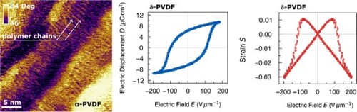
GRAPHICAL ABSTRACT
IMPACT STATEMENT
The capability of atomic force microscopy to investigate surfaces at sub-nanometre scale is applied for a direct observation of polymer chains within the crystalline lamellae at the unit-cell length characteristic.
KEYWORDS:
Introduction
Polyvinylidene fluoride (PVDF) is one of the most attractive ferroelectric polymers thanks to its electroactive properties which originate from the highly polar dipole -CH2CF2- [Citation1]. PVDF finds several applications, including memory device [Citation2,Citation3], tunnel junctions [Citation4–6], sensors [Citation7,Citation8], transistors [Citation9,Citation10] and energy harvesting [Citation11,Citation12]. Five different polymorphs called α-, β-, δ-, γ- and ϵ-phases characterize PVDF. Each of them has a different chain conformation: as TTTT for the β-phase, TGTG’ for α- and δ-phases and T3GT3G’ for γ and ϵ-phases [Citation13]. Solution-processed pristine thin films of PVDF are non-ferroelectric, since the most thermodynamically stable polymorph is the non-polar α-phase [Citation14]. Through different treatments α-PVDF can be converted into electroactive polymorphs [Citation13,Citation15,Citation16]. For instance, δ-PVDF is known as the polar version of the α-phase, since they have the same chain conformation, and can be obtained by electro-forming [Citation14]. By applying high voltage to a non-polar α-phase thin film, a reversal of the dipole components in every second chain occurs, resulting in the molecular packing of the δ-phase [Citation17]. In the α-δ transition the dipoles reversal could be accomplished through several ways. In literature, different possible mechanisms have been discussed, like a reorientation of every second chain by 180° through a propagation of a twist along the molecule, or a 90° rotation about every gauche and gauche minus bond of alternate chains [Citation17–22]. Despite the reversal phenomena, the α-δ transition does not affect molecular conformation TGTG’ and unit-cell dimensions, which remain identical for both phases. The unchanged unit-cell dimensions lead to identical Fourier transforms infrared (FTIR) spectra for both polymorphs. In the same way, X-ray diffraction (XRD) patterns do not show differences in peak positions and only small differences in intensities [Citation14,Citation17]. Ferroelectric characteristics as coercive field and remnant polarization of electro-formed PVDF δ-phase thin films have already been investigated [Citation14]. However, an in-depth and comprehensive electrostrain analysis, i.e. the butterfly curve, for solution-processed thin films and piezoelectric characteristic in the low electric field regime, is still lacking.
In this work, we present a morphological study of PVDF thin films from micro- to sub-nanometre scale using atomic force microscopy (AFM). Starting from the typical PVDF spherulite microstructure, we generated high-resolution morphological maps of the surface at the sub-nanometre scale, which allowed us, for the first time, to observe the polymer chains’ organization inside the crystalline lamellae. FTIR and XRD have been conducted in order to identify the crystalline phase. We report also an electro-mechanical analysis and characterization of the α-δ transition by using micromachined capacitors. Electric displacement and strain characteristics as a function of the electric field have been recorded through stepwise increased electric field applied in order to study the transition from non-polar to polar polymorphic state, and hence, from electrostrictive behaviour to butterfly curve, i.e. the α-δ transition. From this analysis, remnant polarization, coercive field, electrostriction coefficient and piezoelectric coefficient have been determined. Furthermore, we carried out low-field regime measurements by applying an electric field, below the coercive field, demonstrating negative piezoelectric activity depending on the polarized state. We conclude with a comparison between our results and data from literature.
Materials and methods
Synthesis of polymer thin films
The polymer thin films were fabricated via spin-coating from polymer solution. High purity powder, purchased from Sigma-Aldrich, was added with weight ratio of 4% into the solvent dimethylformamide (DMF) at 60°C for increasing the dissolution rate. The polymer solution was spin-coated at 3000 rpm on the substrate which was heated up to 170°C to ensure a smooth and homogeneous surface of the polymer and avoid vapor-induced phase separation [Citation14,Citation23]. Subsequently, the sample was annealed for 2 h at 170°C and cooled down under natural convention. This process led to a film thickness of about 300 nm.
Fabrication of metal-ferroelectric-metal capacitors
For electrical and electro-mechanical characterization of PVDF, micromachined circular shaped capacitors with 6 mm of diameter were fabricated. To start, a 4″ (100) silicon (Si) wafer with 250 nm LPCVD silicon dioxide (SiO2) and 80 nm silicon nitride (Si3N4) layers, needed for electrical insulation, served as substrate. Bottom electrodes were formed by lift-off process, depositing 50 nm of chromium (Cr) by electron-beam evaporation as adhesion promoter for a 100 nm thermally evaporated gold (Au) layer. Afterwards, the polymer was spin-coated and annealed. On top of the polymer, a 150 nm Au layer was thermally evaporated and subsequently patterned by wet chemical etching to serve as top electrode. Details about the microfabrication process can be found in supplementary information (1). Prior to any electro-mechanical characterization, the polymer thin films are polarized by applying sufficiently large DC voltage, meaning above the coercive field.
High-spatial resolution morphological and ferroelectric characterization
The molecular resolution images of PVDF films were obtained by operating an AFM in amplitude modulation mode [Citation24] by applying very small oscillation amplitudes in the range of 100–500 pm to the cantilever. Small and ultra-small amplitudes have already allowed to obtain molecular resolution images of polymer thin films, such as polythiophene [Citation25]. Small amplitude operation enhances the sensitivity to short-range interaction forces and therefore provides a higher spatial resolution. Experiments were performed using PPP-FM-AuD cantilevers (NanoAndMore, Germany) driven in their second flexural mode with typical parameters f2 = 448 kHz, k2 = 158 N m−1 and Q2 = 575. The macroscopic polarization of the material as a function of the electric field was measured via a Sawyer-Tower bridge (see supplementary information (2)). By applying a 10 Hz triangular wave AC signal to the micromachined capacitor and increasing step by step the amplitude, the transition from paraelectric α- to ferroelectric δ-phase has been studied and the hysteretic behaviour was measured, enabling an evaluation of coercive field (Ec) and remnant polarization (Pr). The analysis of the electro-mechanical response has been performed through highly sensitive optical lever readout of a Bruker Dimension Edge AFM. The displacement of the polymer thin film in response to the applied electric field was measured at a single point in the centre of the capacitor. For that purpose, a cantilever (Nanoworld PNP-TR with a spring constant of k = 0.32 N/m) made of silicon nitride (non-conductive cantilever for avoiding electrical interference caused by ground loops) was used. Details of this measurement technique, including a comprehensive discussion on clamping effects, are described elsewhere [Citation26,Citation27].
Results and discussion
Nano- and microstructure of PVDF
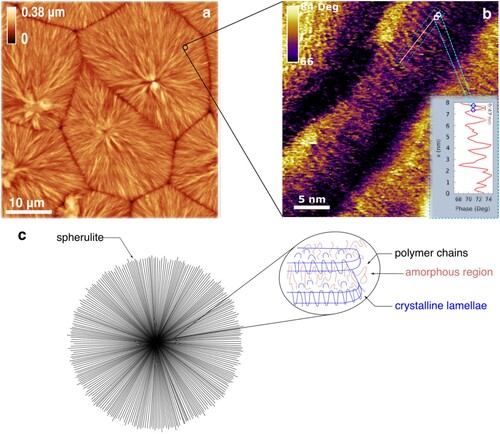
In Figure (a), an AFM height image of the PVDF thin film morphology after annealing is presented, showing typical spherulite microstructure [Citation14]. PVDF crystals growth outward starting from a central nucleation point towards the grain boundary, forming so-called spherulites [Citation27]. Inside the spherulites, polymer chains are orderly packed within platelet-like crystals with a thickness of around 10 nm, called lamellae. Between the lamellae there are gaps where polymer chains are arranged in disordered conformations, resulting in amorphous interlamellar regions [Citation28]. Since a single polymer chain folds back and forth multiple times through the same lamella and/or across different lamellae, crystalline and amorphous parts are strongly intertwined within a single spherulite (see Figure (c)) [Citation27]. PVDF α-phase, arranged in TGTG’ configuration, is characterized by a crystalline unit-cell whose lattice constants are equal to a = 4.96 Å, b = 9.64 Å and c = 4.62 Å [Citation14]. In order to achieve and measure these values, indirect observations have been carried out through spectroscopy techniques, like FTIR and XRD. So far, nobody was able to observe microscopically, so through direct observation, how chains are actually arranged and to measure at the sub-nanometre scale data like the crystalline unit-cell and chain dimension. In Figure (b), we present for the first time a high-resolution AFM phase image in the sub-nanometre regime of a PVDF α-phase thin film that we could use to analyse the packing characteristic of the polymer chains inside a crystalline lamella. The image shows a close-up of the dendrite-like characteristic of the spherulites, already seen in Figure (a) and recognizable in the three raised bands pointing in the same direction, and, most of all, allows us to see the polymer chains arrangement within the crystalline structure of the PVDF α-phase. The AFM measurement section in Figure (b), indicated by a white line drawn perpendicular to the polymer chains, shows the height profile of the raised band surface characterized by distinct ridges. As consequence, we determined at half peak-to-valley height the width of one representative ridge as quantity to measure one polymer chain dimension, resulting in a value of 0.47 nm ( = 4.7 Å). From a projection onto the ab plane of the α-PVDF crystalline unit-cell [Citation17,Citation18], the a-value from these measurements corresponds to the dimension of a polymer chain. The distance peak-to-peak along the y-axis (x(nm)) presented in Figure (b) has been measured in the order of 0.96 nm, therefore in agreement with the b-dimension of the crystalline unit-cell (see supplementary information (3)). Since, as mentioned above, the crystalline unit-cell of PVDF α-phase has lattice constants equal to a = 4.96 Å, b = 9.64 Å and c = 4.62 Å, we have measured for the first time the dimension of a unit-cell through direct microscopic observation. All the ridges on the raised band in Figure (b) are polymer chains packed in parallel within crystalline lamellae. As result of the semi-crystalline nature of PVDF, ordered crystals are characterized also by amorphous parts (see Figure (c)), therefore the profile drawn does not show regular periodicity. Although Figure (b) is associated with PVDF α-phase, since the atomic positions and unit-cell dimensions are identical for both α- and δ-phases [Citation14], it is reasonable to assume that an analogue microscopy-based measurement on the PVDF δ-phase surface would have led to the same crystalline unit-cell value.
Figure 1. Surface morphology of PVDF at the micro-, nanometre and sub-nanometre scale. (a) AFM height image performed at a scan range of 50 µm, which shows the spherulites characterizing the PVDF microstructure. (b) High-resolution AFM height image showing chains organization within a spherulite at the sub-nanometre scale. (c) Schematic illustration of the spherulites structure.
Phase study and molecular conformation
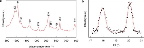
To study and detect the polymer phase of solution-processed thin films, FTIR and XRD have been performed. In Figure (a) the identification of the peaks characterizing the FTIR spectra are presented. The pristine PVDF crystallizes manly into the α-phase, therefore characteristic bands like 615, 764, 795, 855, 976 and 1209 cm−1 are identified [Citation13,Citation29]. No absorption peaks related to γ-phase and β-phase have been found [Citation14,Citation26]. α- and δ-PVDF instead show an identical FITR spectra [Citation14,Citation30–32]. Figure (b) shows the XRD pattern of the solution-processed PVDF thin films. For evaluation of the data, a Split Pearson VII function was fitted to each scattered intensity characteristics to extract peak positions. The 2θ values relating to the peaks are 17.9° and 20.1°, which refer to the (100) and (110) orientation planes of the non-polar TGTG’ α-phase, confirming the observation from the FTIR spectra [Citation14,Citation32–34].
Figure 2. Chain conformation and crystal structure of P(VDF-TrFE). (a) FTIR spectrum (absorbance) and (b) XRD pattern, fitted by a Split Pearson VII, of solution-processed PVDF.
Electro-mechanical characterization
By applying a sufficiently high electric field on a PVDF thin film a transformation from α-PVDF into δ-PVDF occurs. Figure demonstrates the electro-forming process of the δ-phase. The transition is presented through the measured hysteretic response of electric displacement D as a function of electric field E, and electro-mechanical response of strain S as a function of electric field E using micromachined capacitors. The corresponding mechanical strain S = Δl/l0 is calculated as the relative change in thickness of the polymer thin film, where Δl is the variation in thickness from its zero-field value l0 after initial polarization. As presented in Figure , if we start from a pristine film with an applied Emax = 100 Vµm−1, PVDF shows a paraelectric behavior, i.e. α-phase. By increasing E stepwise, the hysteresis and the butterfly curves appear, indicating the transformation into ferroelectric δ-phase. The full D-E loop with a constant Pr is obtained at Emax of about 200 Vµm−1 in conjunction with a stabilized and symmetric S-E curve. In order to evaluate the Ec and Pr from the hysteretic loop, we used an empirical model developed by Miller et al. where two parts composing the hysteresis curve are distinguished: and
[Citation35]. The fitted D-E curve is shown in Figure (a) and the resulting fitting parameters Ec and Pr, equal to 113 Vµm−1 and 6.1 µCcm−2, are mean values of parameters extracted from the two branches, which are in agreement with data previously published [Citation14,Citation36,Citation37]. Furthermore, we studied the Ec and Pr dependency on the frequency applied on the PVDF thin film (see supplementary information (3)). Together with the hysteretic loop, we measured also electrostrain characteristic [Citation26,Citation38]. In general, electrostriction describes the quadratic change of a polarization-induced mechanical strain and, since independent of the crystal class, is present even in amorphous materials [Citation39]. According to the electrostriction model, PVDF piezoelectricity originates from electrostriction and S in ferroelectric polymers varies with the square of D in terms of a Taylor series with the first non-vanishing term [Citation40]:
(1)
(1)
where Q33 is the longitudinal electrostriction coefficient, written with two indices following Voigt’s notation,
is the spontaneous polarization and ϵ = ϵoϵr is the dielectric permittivity [Citation26]. The first term
corresponds to the pure electrostrictive effect, whereas the second one,
, is referred to the linear longitudinal piezoelectric effect, with the piezoelectric coefficient
. The origin of piezoelectricity is attributed to electrostriction biased by spontaneous polarization [Citation24,Citation26,Citation37–39]. The last term,
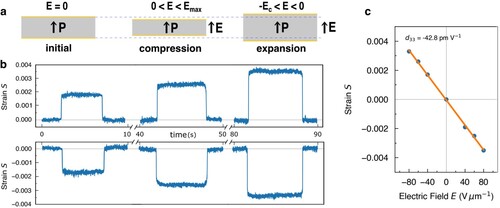
, represents the spontaneous strain. Since a negative Q33 was extracted, the corresponding d33 is negative as well, resulting in values of Q33 = −3.7 m4C−2 and d33 = −39 pmV−1. Similar to the fitting procedure of the D-E hysteresis, two branches can be used. The result from the electrostriction model is compared with measured data and represented in Figure (b). In general, when the electric field applied exceeds the coercive value, the ferroelectric material undergoes polarization reversal, exhibiting a highly non-linear behaviour of the electrostrain, i.e. the butterfly curve [Citation41]. Carrying out measurements at low electric fields, below the coercive value, we can study the piezoelectric nature of the ferroelectric PVDF thin films. PVDF, as its copolymer P(VDF-TrFE), exhibits negative piezoelectricity which arises from the Van der Waals forces acting as intermolecular bonds [Citation42]. Negative piezoelectric behaviour is shown in Figure (a). Applying an electric field along the direction of the polarization results in a contraction of the material, instead, if applied in the opposite direction of the polarization, in an expansion, as long as the field applied is below the coercive field [Citation26,Citation27,Citation42]. However, for proceeding with piezoelectric coefficient analysis, the polymer has to be turned macroscopically into the ferroelectric state [Citation26]. Therefore, we applied an electric field of 150 Vµm−1 for 5 min, since Ec is equal to 113 Vµm−1. Afterwards, we applied different DC voltages, still below coercivity, for an interval of time approximately of 10 s and measured the corresponding lateral displacement of the thin film. The measured data are shown in Figure (a). When an electric field is applied, S moves from zero instantly to a strain value and, once switched off, comes back to the initial zero position. By increasing E, the strain S increases as well. We gathered corresponding E-S pairs and visualized them in an S(E) plot, shown in Figure (c). As expected, the piezoelectric response of the PVDF thin film is linear, and the proportionality factor is d33. Through a linear fit, d33 = −42.8 pmV−1 was extracted, in good agreement with d33 = −39 pmV−1 determined from high fields measurements. The d33 values presented in this work are also comparable to those of biaxially stretched β-PVDF (−31 pm V−1) and solid-state processed PVDF (−36 pm V−1) [Citation36].
Figure 3. D-E (blue) and S-E (red) characteristics as a function of the maximum electric field applied. By increasing the electric field, we have a transformation α- to δ-phase, therefore, from a paraelectric to a ferroelectric behaviour (hysteresis loop).
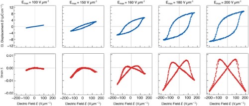
Figure 4. Polarization and ferroelectric characteristics of δ-PVDF. (a) Fit according to the Miller model (grey line) for the measured D-E data (blue circles). (b) Fit according to the electrostrictive model (grey line) for the measured electro-mechanical response (red circles).
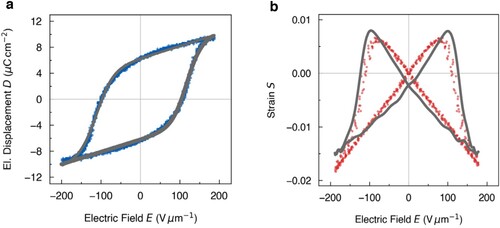
Figure 5. DC step voltage measurements and piezoelectric coefficient estimation. (a) Representation of the negative piezoelectric behaviour. (c) Plot of the S and E values collected from (b) in S as a function of E chart: the linear fitting gives d33.
Conclusion
The spherulite microstructure, typical for α-PVDF has been presented through atomic force microscopy and analysed at the nano- and sub-nanometre scale. By means high-resolution AFM surface imaging, we showed that it is possible to directly observe the crystalline constitution of the polymer. We measured the unit-cell characteristic of PVDF α-phase directly on the polymer surface, finding good agreement with data from literature. Furthermore, we studied ferro- and piezoelectric properties of δ-PVDF thin film and measured Ec = 113 Vµm−1 and Pr = 4.7 µCcm−2. We measured the electro-mechanical behaviour for high fields, recording the highly non-linear electrostrain characteristic and extracted Q33 = −2.4 m4C−2 as well as d33 = −29.8 pmV−1. Low electric field measurements on a polarized thin film showed a linear S-E characteristic that we measured by applying DC voltages and recording the strain due to the piezoelectric response. From that, we obtained d33 = −42.8 pmV−1, in good agreement with measurements for high fields. Next, we compared the data with literature showing how our measurements provided reliable results in terms of ferroelectric activity. The limited number of reports regarding δ-PVDF, especially in terms of electro-mechanical characterization, might be due to the delicate processing, requiring high substrate temperatures and smooth film topographies. Nevertheless, the promising piezoelectric characteristic demonstrated in this work makes the electro-formed δ-PVDF thin films an interesting candidate for several applications in micro electromechanical systems and microelectronics.
Supplemental Material
Download MS Word (4.7 MB)Acknowledgement
The authors acknowledge TU Wien Bibliothek for financial support through its Open Access Funding Program.
Disclosure statement
No potential conflict of interest was reported by the author(s).
Correction Statement
This article has been corrected with minor changes. These changes do not impact the academic content of the article.
Additional information
Funding
References
- Furukawa T. Ferroelectric properties of vinylidene fluoride copolymers. Phase Transitions. 1989;18:143–211.
- Chen X, Han X, Shen QD. PVDF-based ferroelectric polymers in modern flexible electronics. Adv Electron Mater. 2017;3:1600460.
- Guo M, Jiang J, Qian J, et al. Flexible robust and high-density FeRAM from array of organic ferroelectric nano-lamellae by self-assembly. Adv Sci. 2019;6:1801931. Available from: https://onlinelibrary.wiley.com/doi/10.1002advs.201801931
- Garcia V, Bibes M. Ferroelectric tunnel junctions for information storage and processing. Nat Commun. 2014;5:4289.
- López-Encarnación JM, Burton JD, Tsymbal EY, et al. Organic multiferroic tunnel junctions with ferroelectric poly(vinylidene fluoride) barriers. Nano Lett. 2011;11:599–603.
- Kusuma DY, Lee PS. Ferroelectric tunnel junction memory devices made from monolayers of vinylidene fluoride oligomers. Adv Mater. 2012;24:4163–4169.
- Ruan L, Yao X, Chang Y, et al. Properties and applications of the β phase poly(vinylidene fluoride). Polymers (Basel). 2018;10:228.
- Das MS, Mohapatra PC, Aria AI, et al. Piezoelectric materials for energy harvesting and sensing applications: roadmap for future smart materials. Adv Sci. 2021;8:2100864.
- Laudari A, Barron J, Pickett A, et al. Tuning charge transport in PVDF-based organic ferroelectric transistors: status and outlook. ACS Appl Mater Interfaces. 2020;12:26757–26775.
- Georgakopoulos S, Del Pozo FG, Mas-Torrent M. Flexible organic transistors based on a solution-sheared PVDF insulator. J Mater Chem C. 2015;3:12199–12202.
- Costa P, Nunes-Pereira J, Pereira N, et al. Recent progress on piezoelectric, pyroelectric, and magnetoelectric polymer-based energy-harvesting devices. Energy Technol. 2019;7:1–19.
- Wang Y, Zhu X, Zhang T, et al. A renewable low-frequency acoustic energy harvesting noise barrier for high-speed railways using a Helmholtz resonator and a PVDF film. Appl Energy. 2018;230:52–61. doi:10.1016/j.apenergy.2018.08.080
- Martins P, Lopes AC, Lanceros-Mendez S. Electroactive phases of poly(vinylidene fluoride): determination, processing and applications. Prog Polym Sci. 2014;39:683–706. doi:10.1016/j.progpolymsci.2013.07.006
- Li M, Wondergem HJ, Spijkman MJ, et al. Revisiting the δ-phase of poly(vinylidene fluoride) for solution-processed ferroelectric thin films. Nat Mater. 2013;12:433–438.
- Sencadas V, Gregorio R, Lanceros-Méndez S. Α to β phase transformation and microestructural changes of PVDF films induced by uniaxial stretch. J Macromol Sci Part B Phys. 2009;48:514–525.
- Park JH, Kurra N, AlMadhoun MN, et al. A two-step annealing process for enhancing the ferroelectric properties of poly(vinylidene fluoride) (PVDF) devices. J Mater Chem C. 2015;3:2366–2370.
- Davis GT, McKinney JE, Broadhurst MG, et al. Electric-field-induced phase changes in poly(vinylidene fluoride). J Appl Phys. 1978;49:4998–5002.
- Scheinbeim JI, Yoon CH, Pae KD, et al. Poling-time dependence of the field-induced phase transition and piezoelectric response of poly(vinylidene fluoride) films. J Polym Sci Polym Phys Ed. 1980;18:2271–2276. Available from: https://onlinelibrary.wiley.com/doi/10.1002pol.1980.180181111
- Naegele D, Yoon DY, Broadhurst MG. Formation of a new crystal form (α p) of poly(vinylidene fluoride) under electric field. Macromolecules. 1978;11:1297–1298. Available from: https://pubs.acs.org/doi/abs/10.1021ma60066a051
- Dvey-Aharon H, Taylor PL, Hopfinger AJ. Dynamics of the field-induced transition to the polar α phase of poly(vinylidene fluoride). J Appl Phys. 1980;51:5184–5187.
- Hasegawa R, Takahashi Y, Chatani Y, et al. Crystal structures of three crystalline forms of poly(vinylidene fluoride). Polym J. 1972;3:600–610.
- Bachmann MA, Lando JB. A reexamination of the crystal structure of phase II of poly(vinylidene fluoride). Macromolecules. 1981;14:40–46.
- Li M, Katsouras I, Piliego C, et al. Controlling the microstructure of poly(vinylidene-fluoride) (PVDF) thin films for microelectronics. J Mater Chem C. 2013;1:7695–7702.
- Garcia R. Amplitude modulation atomic force microscopy. Weinheim: Wiley-VC Verlag GmbH & Co. KGaA; 2010.
- Korolkov VV, Summerfield A, Murphy A, et al. Ultra-high resolution imaging of thin films and single strands of polythiophene using atomic force microscopy. Nat Commun. 2019;10:1537. Available from: http://www.nature.com/articles/s41467-019-09571-6
- Hafner J, Benaglia S, Richheimer F, et al. Multi-scale characterisation of a ferroelectric polymer reveals the emergence of a morphological phase transition driven by temperature. Nat Commun. 2021;12:1–9. doi:10.1038/s41467-020-20407-6
- Katsouras I, Asadi K, Li M, et al. The negative piezoelectric effect of the ferroelectric polymer poly(vinylidene fluoride). Nat Mater. 2016;15:78–84.
- Kepler RG, Anderson RA. Ferroelectric polymers. Adv Phys. 1992;41:1–57.
- Benz M, Euler WB, Gregory OJ. The role of solution phase water on the deposition of thin films of poly(vinylidene fluoride). Macromolecules. 2002;35:2682–2688.
- Lovinger AJ. Molecular mechanism for α-γ transformation in electrically poled poly(vinylidene fluoride). Macromolecules. 1981;14:225–227.
- Bachmann M, Gordon WL, Weinhold S, et al. The crystal structure of phase IV of poly(vinylidene fluoride). J Appl Phys. 1980;51:5095–5099.
- Wang TT, West JE. Polarization of poly(vinylidene fluoride) by application of breakdown fields. J Appl Phys. 1982;53:6552–6556. Available from: http://aip.scitation.org/doi/10.10631.330075
- Das Gupta DK, Doughty K. Changes in x-ray diffraction patterns of polyvinylidene fluoride due to corona charging. Appl Phys Lett. 1977;31:585–587.
- Das-Gupta DK, Doughty K. Corona charging and the piezoelectric effect in polyvinylidene fluoride. J Appl Phys. 1978;49:4601–4603.
- Miller SL, Nasby RD, Schwank JR, et al. Device modeling of ferroelectric capacitors. J Appl Phys. 1990;68:6463–6471.
- Martín J, Zhao D, Lenz T, et al. Solid-state-processing of δ-PVDF. Mater Horizons. 2017;4:408–414.
- Li M, Katsouras I, Asadi K, et al. Low voltage extrinsic switching of ferroelectric δ-PVDF ultra-thin films. Appl Phys Lett. 2013;103:072903.
- Hafner J, Teuschel M, Schneider M, et al. Origin of the strong temperature effect on the piezoelectric response of the ferroelectric (co-)polymer P(VDF 70 -TrFE 30). Polymer. 2019;170:1–6. doi:10.1016/j.polymer.2019.02.064
- Hafner J, Teuschel M, Disnan D, et al. Large bias-induced piezoelectric response in the ferroelectric polymer P(VDF-TrFE) for MEMS resonators. Mater Res Lett. 2021;9:195–203. doi:10.1080/21663831.2020.1868593
- Furukawa T, Seo N. Electrostriction as the origin of piezoelectricity in ferroelectric polymers. Jpn J Appl Phys. 1990;29:675–680.
- Furukawa T, Nakajima K, Koizumi T, et al. Measurements of nonlinear dielectricity in ferroelectric polymers. Jpn J Appl Phys. 1987;26:1039–1045. Available from: https://iopscience.iop.org/article/10.1143JJAP.26.1039
- You L, Zhang Y, Zhou S, et al. Origin of giant negative piezoelectricity in a layered van der Waals ferroelectric. Sci Adv. 2019;5:1–10. doi:10.1126/sciadv.aav3780