
 ?Mathematical formulae have been encoded as MathML and are displayed in this HTML version using MathJax in order to improve their display. Uncheck the box to turn MathJax off. This feature requires Javascript. Click on a formula to zoom.
Abstract
Aluminum scandium nitride (AlScN) has been receiving increasing interest for radio frequency microelectromechanical systems because of their higher achievable bandwidths owing to the larger piezoelectric response of AlScN compared to AlN. However, alloying scandium (Sc) with aluminum nitride (AlN) significantly lowers the thermal conductivity of AlScN due to phonon alloy scattering. Self-heating in AlScN devices potentially limits power handling, constrains the maximum transmission rate, and ultimately leads to thermal failure. We grew plasma-assisted molecular beam epitaxy (PAMBE) AlScN on AlN-Al2O3 and GaN-Al2O3 substrates, and compared the cross-plane thermal conductivity to current work on AlScN grown on Si substrates.
GRAPHICAL ABSTRACT
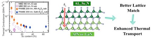
IMPACT STATEMENT
AlScN grown on AlN-Al2O3 and GaN-Al2O3 substrates achieve a better lattice match and a comparable thermal conductivity to AlScN grown on Si substrates, but with significantly thinner films.
1. Introduction
Aluminum scandium nitride (AlScN) has gained increasing attraction for use as an active epitaxial layer in GaN-based high-power radio frequency (RF) and mm-wave devices due to its strong piezoelectric and spontaneous polarization and lattice-matching with GaN for Sc content < 18% [Citation1,Citation2]. This allows for tunable barrier thicknesses and epitaxial strain management and higher on-currents and output power densities due to a larger carrier concentration in the polarization-induced two-dimensional electron gas (2DEG) in AlGaN/AlScN/GaN, compared to traditional AlGaN/GaN HEMTs [Citation3,Citation4]. In addition, RF microelectromechanical systems (MEMS) based on AlScN are replacing AlN-based devices because of AlScN’s larger piezoelectric response relative to AlN, which leads to higher achievable bandwidths [Citation5]. As a result, manufacturers have recently started utilizing AlScN as the piezoelectric material in film bulk acoustic resonators (FBARs) [Citation5]. Nonetheless, to handle high operational frequencies, an FBAR’s physical size typically decreases, while higher RF input powers are required to counter signal attenuation, thereby leading to an increased operational heat flux [Citation5]. Although AlN has a large bulk thermal conductivity of 320 (W/m-K), [Citation6] adding Sc to AlN drastically decreases the thermal conductivity [Citation5,Citation7,Citation8]. Self-heating in AlScN FBARs potentially limits power handling, constrains the maximum transmission rate, and ultimately leads to thermal failure [Citation5].
Recent work on AlScN has been based on growing the layer on silicon (Si) substrates for MEMS applications [Citation5,Citation7,Citation8]. However, the significant lattice mismatch between Si and AlScN can decrease the quality of the film and thereby result in increased operational temperatures. To mitigate thermal failure and guide its future use in devices, it is necessary to understand and enhance the thermal transport properties of AlScN thin films to ensure the higher power handling capability is not compromised by inefficient heat removal. In this work, we grew 200 nm plasma-assisted molecular beam epitaxy AlScN on AlN-Al2O3 substrates and GaN-Al2O3 substrates and measured the cross-plane thermal conductivity utilizing the pump–probe method of frequency-domain thermoreflectance. We observed comparable thermal conductivity to AlScN grown on Si substrate, but with 50% to 75% thinner AlScN films.
2. Materials and methods
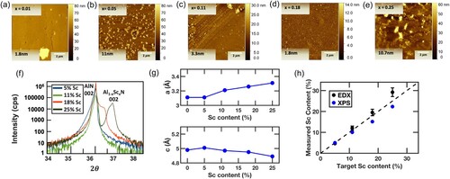
The Al1-xScxN/AlN-Al2O3 heterostructures; x = 0.01, 0.05, 0.11, 0.18 and 0.25; were grown by plasma-assisted molecular beam epitaxy (PAMBE) in a Veeco GenXplor system on AlN-Al2O3 substrates. Growth characterization of atomic force microscopy (AFM), x-ray diffraction (XRD), reciprocal space mapping (RSM), energy-dispersive x-ray (EDX) spectroscopy, and x-ray photoelectron spectroscopy (XPS) measurements are provided in Figure . XRD shows the AlN and the AlScN peaks Figure (f). RSM measurements were taken to determine the lattice parameters of 200 nm thick wurtzite AlScN films grown on AlN, Figure (g). As shown in Figure (g), the non-monotonic trend of the out-of-plane, or lattice parameter as a function of Sc content is due to two competing effects: (1) larger bond length of Sc-N than Al-N tends to increase both
and
lattice parameters (2) due to different crystalline structure between ScN and AlN, as Sc is introduced, the tetrahedral bonds are rotated into the plane, causing an increasing
but decreasing
. Lastly, true Sc content was determined through EDX spectroscopy (bulk values) and XPS (surface values), Figure (h).
Figure 1. AFM images of AlScN on AlN-Al2O3 substrate with Sc composition (a) x = 0.01, (b) x = 0.05, (c) x = 0.11, (d) x = 0.18 and (e) x = 0.25. (f) 002 omega-2theta XRD scans. (g) In-plane, a, and out-of-plane, c, lattice parameters of 200 nm thick wurtzite AlScN films grown on AlN-Al2O3 substrates, determined by RSM measurements. (h) Measured versus target Sc content of 200 nm thick AlScN films. The true Sc content was measured by EDX spectroscopy (bulk values) and XPS (surface values).
The Al1-xScxN/GaN-Al2O3 heterostructures; x = 0.18, 0.23, 0.28, 0.35, and 0.65; were grown on a Veeco GENXplore PAMBE system with conventional Al, Ga and Sc effusion cells and a radio-frequency (RF) plasma source to supply active nitrogen. A 200 nm GaN buffer layer was grown in-situ on 11 cm2 GaN-Al2O3 substrate right before the growth of AlScN. Growth characterization of high-resolution XRD, AFM, and EDX spectroscopy are provided in the Figure . A Veeco Dimension ICON AFM was employed to characterize the surface morphology of the samples. Smooth surface morphology was obtained for the AlScN films as shown in the 5 μm × 5 μm AFM images, Figure (a–e). As shown in Figure (a), spiral atomic steps were observed at low Sc composition (x = 0.18) indicating that the AlScN layer followed the morphology of underlaying GaN layer [Citation9]. However, the atomic steps degraded into high density grains for high (x = 0.65) Sc composition, Figure (e). High-resolution XRD
-
scans were recorded on Rigaku Smartlab XRD. The XRD plot presented in Figure (f) clearly shows the GaN and the AlScN peaks. This also confirms the pure wurtzite phase of AlScN present in the samples. Further, the specifics of the growth procedure for Al1-xScxN/GaN-Al2O3 and Al1-xScxN/AlN-Al2O3 are provided in the Supplementary Material.
Figure 2. AFM image of AlScN on GaN-Al2O3 substrate with Sc composition (a) x = 0.18, (b) x = 0.23, (c) x = 0.28, (d) x = 0.35 and (e) x = 0.65. The bright spots in the AFM images are dislocations which include mixed and screw dislocations [Citation10]. (f) High-resolution XRD plot of AlScN with Sc composition. (g) Measured versus target Sc content of AlScN on GaN-Al2O3 substrates, measured by EDX.
![Figure 2. 5μm×5μm AFM image of AlScN on GaN-Al2O3 substrate with Sc composition (a) x = 0.18, (b) x = 0.23, (c) x = 0.28, (d) x = 0.35 and (e) x = 0.65. The bright spots in the AFM images are dislocations which include mixed and screw dislocations [Citation10]. (f) High-resolution XRD plot of AlScN with Sc composition. (g) Measured versus target Sc content of AlScN on GaN-Al2O3 substrates, measured by EDX.](/cms/asset/f6ce659e-22ec-46ad-af52-c75f02f75961/tmrl_a_2279667_f0002_oc.jpg)
We measured the cross-plane thermal conductivity (k⊥) of AlScN thin films using the optical pump–probe method of frequency-domain thermoreflectance (FDTR). The electro-optic modulator induced an intensity modulation on the 488 nm continuous wave laser, generating a periodic heat flux on the sample surface [Citation11]. An unmodulated, 532 nm continuous wave laser monitored the surface temperature through a change in surface reflectivity (Figure S2) [Citation12]. The measurement of individual material physical properties was performed as an inverse problem, minimizing the error between measured lock-in phase data and the calculated phase via a nonlinear least-squares algorithm [Citation12]. An instance of the phase versus frequency data attained from FDTR of an average of three runs collected at a specific location is depicted in Figure S3. The best fit curve closely approximates the data, derived by solving the heat diffusion equation. Schmidt et al. have provided a more detailed explanation of how this equation is solved [Citation12]. We previously applied FDTR to study homoepitaxial AlN and pulsed laser deposited h-BN [Citation6,Citation13]. Further, the specifics of the experimental setup are provided in the Supplementary Material. Each measured k⊥ data was an average of three measurements on three different locations on the sample e.g. total of nine measurements.
3. Results and discussion
We investigated the cross-plane thermal conductivity (k⊥), hereafter denoted as k, of AlScN thin films grown on different high k materials (i.e. AlN and GaN). The Al1-xScxN layer of 200 nm thick was grown at various Sc content. Specifically, the AlScN/AlN-Al2O3 samples were grown at x 0.01, 0.05, 0.11, 0.18 and 0.25 Sc, while the AlScN/GaN-Al2O3 samples were grown at x
0.18, 0.23, 0.28, 0.35, and 0.65 Sc. Lattice parameters for AlScN and substrates of AlN, GaN, and Si are shown in Figure (a), in which the lattice mismatch is calculated as
where
and
are the in-plane lattice parameters of the AlScN film and the substrate, respectively. Although mixed phases of AlN (wurtzite) and ScN (rock salt) are prevalent for x > 0.40 Sc as shown in Figure (b), [Citation14] we were interested in measuring the thermal conductivity across a wide range of alloy compositions to determine if the k follows the typical alloyed trend.
Figure 3. (a) Lattice parameters of AlScN, AlN and GaN structures explored in this work. AlN and GaN wurtzite structures have a lattice mismatch of 4% and 2% with Al1−xScxN, respectively. Si lattice parameters are shown as a reference for current k literature of large lattice mismatched Al1−xScxN/Si heterostructures. Si (001) rock salt structure [Citation15] induces a large lattice mismatch of 40% with the AlScN wurtzite structure, while Si (111) results in a larger lattice mismatch of 51% [Citation16]. (b) Mixed phases of AlN (wurtzite) and ScN (rock salt) are prevalent for x > 0.40 Sc. After the critical Sc content x > 0.56, Al1−xScxN prefers the rock salt structure.
![Figure 3. (a) Lattice parameters of AlScN, AlN and GaN structures explored in this work. AlN and GaN wurtzite structures have a lattice mismatch of 4% and 2% with Al1−xScxN, respectively. Si lattice parameters are shown as a reference for current k literature of large lattice mismatched Al1−xScxN/Si heterostructures. Si (001) rock salt structure [Citation15] induces a large lattice mismatch of 40% with the AlScN wurtzite structure, while Si (111) results in a larger lattice mismatch of 51% [Citation16]. (b) Mixed phases of AlN (wurtzite) and ScN (rock salt) are prevalent for x > 0.40 Sc. After the critical Sc content x > 0.56, Al1−xScxN prefers the rock salt structure.](/cms/asset/cbf2b06f-4730-4379-8d7d-16469ba250da/tmrl_a_2279667_f0003_oc.jpg)
The observed decline in k of AlScN due to alloying aligns with the prevailing findings in previous experimental studies of various alloyed materials, such as AlxGa1-xN, InxGa1-xN and InxAl1-xN, as shown in Figure . But AlScN shows a steeper drop at the dilute limit. At 1% Sc, the k drop is already 75%. We think this can be attributed to the more severe lattice disruption. Unlike the other alloy systems, AlN and ScN have intrinsically different crystal structures—wurtzite and rocksalt, respectively. The introduction of Sc not only introduces mass disorder but also has a stronger force constant disorder given the tendency to disrupt the original crystal structure. In other words, Sc atoms are less comfortable sitting on a wurtzite lattice site, compared to Ga atoms introduced to AlN, as GaN itself also has a wurtzite structure. In addition, in AlScN the Sc-N bonds are on average longer than the Al-N bonds and more ionic in nature. This results in a decrease in the elastic stiffness coefficient and an increase in the piezoelectric stress coefficient [Citation5]. As a result, as Sc atomic percent increases, the acoustic phonon (primary heat carriers) group velocities decrease and phonon-alloy scattering increases, thereby depleting the thermal conductivity, as shown in Figure .
Figure 4. (a) Thermal conductivity (k) as a function of mass fraction. k of PAMBE-grown Al1−xScxN on AlN-Al2O3 substrates (filled orange diamonds) and on GaN-Al2O3 substrates (filled blue diamonds) to mass fraction, x. AlxGa1-xN (unfilled black), [Citation17–20] InxGa1-xN (unfilled green circles), [Citation19–21] and InxAl1-xN (unfilled blue squares) [Citation20–22] literature results are shown for comparison. As the mass fraction x is increased, the typical U-shaped alloy k behavior of an abrupt reduction in k, followed by a gradual approach to a minimum, and finally a rapid increase in k is followed by Al1−xScxN (blue trendline shown to guide reader’s eyes), similar to that of AlxGa1-xN (gray trendline). (b) Results shown in log-scale to better distinguish our results with current literature. Inset shows AlScN grown on either AlN-Al2O3 or GaN-Al2O3 substrates.
![Figure 4. (a) Thermal conductivity (k) as a function of mass fraction. k of PAMBE-grown Al1−xScxN on AlN-Al2O3 substrates (filled orange diamonds) and on GaN-Al2O3 substrates (filled blue diamonds) to mass fraction, x. AlxGa1-xN (unfilled black), [Citation17–20] InxGa1-xN (unfilled green circles), [Citation19–21] and InxAl1-xN (unfilled blue squares) [Citation20–22] literature results are shown for comparison. As the mass fraction x is increased, the typical U-shaped alloy k behavior of an abrupt reduction in k, followed by a gradual approach to a minimum, and finally a rapid increase in k is followed by Al1−xScxN (blue trendline shown to guide reader’s eyes), similar to that of AlxGa1-xN (gray trendline). (b) Results shown in log-scale to better distinguish our results with current literature. Inset shows AlScN grown on either AlN-Al2O3 or GaN-Al2O3 substrates.](/cms/asset/51ad4c2a-c117-49d4-81be-cd40a0fd8781/tmrl_a_2279667_f0004_oc.jpg)
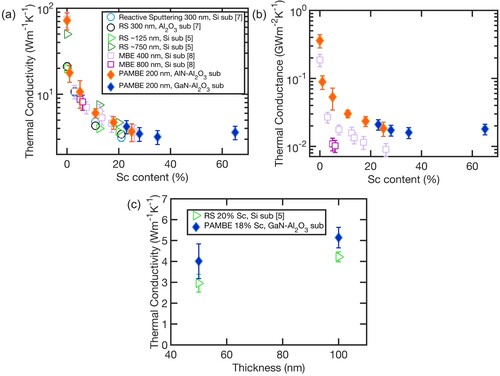
We then compared our PAMBE-grown AlScN/AlN-Al2O3 and AlScN/GaN-Al2O3 with reactive sputter (RS) and MBE-grown AlScN/Si in Figure (a). Based on the size effect, we should expect a thinner sample to have a smaller k if the sample quality remains the same. Notably, at 5% Sc, the k for our thinner, 200 nm PAMBE-grown Al1−xScxN/AlN-Al2O3 is 11 (W/m-K); while the k for the thicker, 800 nm Al1−xScxN/Si is 9 (W/m-K). Similarly, at a 18% Sc, our thinner, 200 nm PAMBE-grown Al1−xScxN/AlN-Al2O3 displays a k [4.7 (W/m-K)] comparable to that for the thicker, 400 nm MBE-grown Al1−xScxN/Si at a lower Sc atomic percent of 16% [∼4.5 (W/m-K)]. This trend is followed at higher Sc atomic contents. This means we can achieve a comparable to enhanced k, with 50% to 75% thinner AlScN films.
Figure 5. (a) The thermal conductivity (k) of Al1−xScxN/AlN-Al2O3 and Al1−xScxN/GaN-Al2O3 compared to reactive sputtered or MBE grown Al1−xScxN/Si and Al1−xScxN/Al2O3 films based on Sc atomic percentage. (b) Thermal conductance; k divided by thickness of the respective Al1−xScxN thin film. Al1−xScxN films grown on high k AlN and lattice matched GaN (filled orange and blue diamonds, respectively) results in the highest thermal conductance values. (c) Thickness dependent k, as the thickness of the AlScN/GaN-Al2O3 decreases, the k also decreases due to high phonon boundary scattering. Reactive sputter deposited AlScN/Si is shown in green for comparison.
To investigate the effect of mixed phases beyond the critical Sc content of 56% where AlScN prefers the rock salt structure, [Citation14] we also measured a 65% Sc sample. Our k results appear to commence forming the ‘U’ shape prominent in alloyed systems such as Al1−xGaxN. Although industry concerns are focused on Sc atomic percent below 40% where the wurtzite phase can be stabilized, [Citation2] it is important to capture the alloyed behavior of AlScN across a large range in the alloy system.
Given the size effect, we plotted the k normalized by the AlScN layer thickness to obtain a thermal conductance G (GW/m2-K) vs Sc atomic percent. As shown in Figure (b), the samples from this work provide the highest G for PAMBE-grown Al1−xScxN thin films to date.
To further investigate the thickness dependence on k for Al1−xScxN, 50 nm and 100 nm thick samples were grown with 18% Sc. At 18% Sc, Al0.82Sc0.18N is lattice matched to GaN [Citation14] and should, in theory, result in the highest k compared to Al0.82Sc0.18N/AlN and Al0.82Sc0.18N/Si(001) with a lattice mismatch of 4% and 40%, respectively. Thus, Al0.80Sc0.20N/Si samples grown by reactive sputtering are compared to this work’s Al0.82Sc0.18N/GaN-Al2O3 films [Citation5]. This allows a direct k comparison of Al1−xScxN on different substrates at the same thickness. Clearly, with a better lattice match, Al1−xScxN/GaN-Al2O3 shows a higher thermal conductivity than Al1−xScxN/Si, as shown in Figure (c). Moreover, the thermal conductivity increases with increasing thickness. As previously noted, strong alloy scattering diminishes k, yet k is further strongly impacted by a decrease in thickness as phonon boundary scattering takes place, as shown in Figure (c).
5. Conclusions
In conclusion, PAMBE-grown AlScN films with 50% to 75% thinner thicknesses on AlN-Al2O3 or GaN-Al2O3 substrates demonstrate comparable cross-plane thermal conductivity to reactive sputtered or MBE-grown AlScN on Si substrates. The growth of wurtzite structure AlScN on lattice matched GaN improves the quality of the film and enhances thermal transport, rather than growth on the face-centered diamond cubic structure of Si. In addition, the thermal conductivity of AlScN versus Sc contents shows a similar U-shape due to phonon-alloying scattering compared other alloys, however, the reduction of k is more pronounced in the dilute limit for AlScN due to the tendency for lattice disruption. These findings help enhance the understanding of the thermal transport properties of AlScN and its corresponding nitride heterostructures and ultimately have significant implications for the use of AlScN in acoustic, power electronic, and high-speed microwave applications where heat management is critical to device performance.
Supplemental Material
Download MS Word (4.4 MB)Acknowledgement
G. A. Alvarez was sponsored by the GEM Associate Ph.D. Fellowship. This work was performed, in part, at the Cornell NanoScale Facility, a member of the National Nanotechnology Coordinated Infrastructure (NNCI), which is supported by the National Science Foundation (Grant No. NNCI-2025233). The authors would like to thank Cindy Lee and Zhaobo Mei for the AFM and XRD. The authors would like to thank Jonas Lähnemann at the Paul Drude Institute for Solid State Electronics for helpful discussions.
Disclosure statement
No potential conflict of interest was reported by the author(s).
Data availability
The data that support the findings of this study are available from the corresponding author upon reasonable request.
Additional information
Funding
References
- Hardy MT, Downey BP, Nepal N, et al. Epitaxial ScAlN grown by molecular beam epitaxy on GaN and SiC substrates. Appl Phys Lett. 2017;110:162104. doi:10.1063/1.4981807
- Zhang S, Fu WY, Holec D. Elastic constants and critical thicknesses of ScGaN and ScAlN. J Appl Phys. 2013;114:243516. doi:10.1063/1.4848036
- Tahhan MB, Logan JA, Hardy MT, et al. Passivation schemes for ScAlN-barrier mm-wave high electron mobility transistors. IEEE Trans Electron Dev. 2022;69(3):962–967. doi:10.1109/ted.2021.3140016
- Kazior TE, et al. High power density ScAlN-based heterostructure FETs for mm-wave applications. in IEEE MTT-S International Microwave Symposium Digest vols 2019-June 1136–1139. Institute of Electrical and Electronics Engineers Inc., 2019.
- Song Y, Perez C, Esteves G, et al. Thermal conductivity of aluminum scandium nitride for 5G mobile applications and beyond. ACS Appl Mater Interfaces. 2021;13:19031–19041.
- Alvarez-Escalante G, Page R, Hu R, et al. High thermal conductivity and ultrahigh thermal boundary conductance of homoepitaxial AlN thin films. APL Mater. 2022;10:011115. doi:10.1063/5.0078155
- Tran DQ, Tasnádi F, Žukauskaitė A, et al. Thermal conductivity of ScxAl1−xN and YxAl1−xN alloys. Appl. Phys. Lett. 2023;122:182107. doi:10.1063/5.0145847
- Yuan C, Park M, Zheng Y, et al. Phonon heat conduction in Al1-xScxN thin films. Mater Today Phys. 2021;21.
- Wang P, Arto Laleyan D, Pandey A, et al. Molecular beam epitaxy and characterization of wurtzite ScxAl1−xN. J Appl Phys. 2020;116:151903.
- Hao M, et al. Study of threading dislocations in wurtzite GaN films grown on sapphire by metalorganic chemical vapor deposition. Jpn J Appl Phys. 1998;37.
- Regner KT, Majumdar S, Malen JA. Instrumentation of broadband frequency domain thermoreflectance for measuring thermal conductivity accumulation functions. Rev Sci Instrum. 2013;84:064901. doi:10.1063/1.4808055
- Schmidt AJ, Cheaito R, Chiesa M. A frequency-domain thermoreflectance method for the characterization of thermal properties. Rev Sci Instrum. 2009;80:94901. doi:10.1063/1.3212673
- Alvarez GA, Christiansen-Salameh J, Biswas A, et al. Cross-plane thermal conductivity of h-BN thin films grown by pulsed laser deposition. J Appl Phys. 2023;122:232101.
- Moram MA, Zhang S. ScGaN and ScAlN: emerging nitride materials. J Mater Chem A. 2014;2; doi:10.1039/C3TA14189F
- Jain A, Ong SP, Hautier G, et al. Commentary: the materials project: a materials genome approach to accelerating materials innovation. APL Mater. 2013;1:11002. doi:10.1063/1.4812323
- Nakanishi S, Horiguchi T. Surface lattice constants of Si(111), Ni(111) and Cu(111). Jpn J Appl Phys. 1981;20:L214–L216. doi:10.1143/JJAP.20.L214
- Slomski Joseph M. Thermal conductivity of group-III nitrides and oxides. North Carolina State University; 2017.
- Filatova-Zalewska A, Litwicki Z, Suski T, et al. Thermal conductivity of thin films of gallium nitride, doped with aluminium, measured with 3ω method. Solid State Sci. 2020;101; doi:10.1016/j.solidstatesciences.2019.106105
- Adachi S. Lattice thermal conductivity of group-IV and III-V semiconductor alloys. J Appl Phys. 2007;102.
- Vitanov S. Simulation of high electron mobility transistors. Technische Universität Wien; 2010.
- Pantha BN, Dahal R, Li J, et al. Thermoelectric properties of InxGa1−xN alloys. Appl Phys Lett. 2008;92:042112. doi:10.1063/1.2839309
- Yamaguchi S, Izaki R, Yamagiwa K-i, et al. Thermal diffusivity and thermoelectric figure of merit of Al1-xInxN prepared by reactive radio-frequency sputtering. Appl Phys Lett. 2003;83:5398–5400. doi:10.1063/1.1637156