
ABSTRACT
Amorphous-nanocrystalline (a-nc) boron carbide thin films were prepared by chemical vapor deposition (CVD) by using ortho-carborane as a single-source precursor for inertial confinement fusion (ICF) application. The effects of deposition temperature (Tdep) and total pressure (Ptot) on chemical composition, microstructure, stoichiometry and morphology of the boron carbide films were investigated. The TEM results show that the structure of the film is mainly composed of amorphous boron carbide with dispersive nano-grains, which will be able to improve the mechanical properties of the film with relatively low roughness. The hardness of the (a-nc) boron carbide film obtained in this study reached 20.6 GPa, and roughness of 3.21 nm. The deposited films sized 0.2–1.9 μm in thickness with B/C atomic ratio ranged from 0.14 to 3.29. The deposition rate decreased with increasing deposition temperature and Ptot, while B/C ratio increased.
1. Introduction
Inertial confinement fusion (ICF) has been extensively studied and developed since it is a dependable choice to provide clean and sustainable energy. In the research of ICF, the design and manufacture of ignition capsules are an extremely important part. Boron carbide is a low Z material with a series of excellent properties such as low density, high thermal neutron capture cross-section, high melting point, high thermal and chemical stability [Citation1–Citation6]. These properties make boron carbide a potential ablation material for ICF capsules applications.
summarizes the investigations on boron carbide films deposited by PVD and CVD. A variety of techniques have been developed to fabricate boron-carbide films. Chemical vapor deposition (CVD) methods have been widely used for boron carbide films due to the better controlled deposition process and the high-quality boron carbide production [Citation7–Citation9]. CVD of boron carbide films is typically conducted at high temperatures using simple hydrocarbons (CH4) and chlorides (BCl3) of boron as precursors. Reaction gas mixtures such as BI3-CH4, BCl3-CH4-H2, BBr3-CH4-H2 and BCl3-CCl4-H2 are most commonly adapted to conduct boron carbide films [Citation10–Citation12]. As chlorides are hazardous and synthesis process requires high temperature, replacing conventional chlorinated precursors with highly reactive organoboranes has become a trend in recent years [Citation13]. The small organoboron molecules such as trimethylboron, B(CH3)3 (TMB) and triethylboron, B(C2H5)3 (TEB) routes seem promising but will face the problem that small molecules were found to be over-reactive. As ortho-carborane (C2H12B10) has the highest B/C ratio of common organoboron precursors, it is seemingly an attractive choice for preparing boron carbide films.
Table 1. Reports of boron carbide films by PVD and CVD methods.
Of the many types of CVD processes, plasma-enhanced chemical vapor deposition (PECVD) has been extensively used to fabricate boron carbide films because high internal energy state of plasma enhances the chemical reaction rate of the precursor. However, this plasma process could cause damage to the surface of the substrate due to the energetic ions. Thermal chemical vapor deposition technique, in some cases, is even better than PECVD processes due to its design simplicity, lower ownership cost and better control of deposition process. However, thermal CVD using ortho-carborane to prepare boron carbide films was not widely adopted or studied. In addition, most of the boron carbide films prepared by CVD reported were amorphous, and there were few reports of nanocrystalline boron carbide films.
Nanocrystallization of amorphous materials can disperse nanocrystals in an amorphous matrix to form nanocrystalline/amorphous composites, thereby improving the mechanical/physical properties of films [Citation19]. On the other hand, as the crystal grains size increase, the film roughness increases. However, due to the amorphous-nanocrystalline structure, the (a-nc) boron carbide film has a low roughness, which is advantageous for reducing the Rayleigh Taylor instability during the ablation process [Citation20].
In this work, amorphous-nanocrystalline (a-nc) boron carbide films were deposited using ortho-carborane as a single precursor by thermal CVD. The effects of deposition temperature and total pressure on chemical composition, microstructure, stoichiometry and morphology of boron carbide thin films were investigated.
2. Experimental
A thermal Chemical Vapor Deposition system was used for the film deposition on fused quartz substrates. Quartz glass substrates, 15 × 10 × 0.5 mm3 in size, were ultrasonically cleaned with acetone and deionized (DI) water for 20 and 10 min, and then blown dry with N2 stream. Subsequently, substrates were placed on a quartz boat and loaded into the deposition chamber. Ortho-carborane (C2H12B10, 98.0%, Zhengzhou Alfa Chemical Co., Ltd., Zhengzhou, China) is served as a single-source precursor supplying both boron and carbon atoms to the deposition process. Each process is started by establishing an Ar (Wuhan Xiangyun Chemical Co., Ltd., Wuhan, China, 99.999%) flow of 100 sccm into the evacuated chamber for 30 min to degas the chamber walls. Subsequently, o-carborane was vaporized at 220°C and introduced into the CVD chamber, signifying the start of the film deposition. Depositions were carried out under pressure 100–50,000 Pa, temperature 900–1200°C. The deposition time is set to 30 min. After deposition, the furnace was naturally cooled down to room temperature by an Ar flow of 100 sccm.
X-ray diffraction microscopy (XRD; Ultima III, Rigaku, Tokyo, Japan, at 40 kV and 40 mA) and Transmission electron microscopy (TEM, JEOL Ltd., Tokyo, Japan, JEM-3010, 200 kV) were used to characterize the microstructure of boron carbide films. A field-emission scanning electron microscope (SEM; Quanta-250, FEI, Houston, TX, at 20 kV) was used to observe the film thickness and morphology, and the deposition rate (Rdep) was calculated from the deposits thickness and deposition time. X-ray photoelectron spectroscopy (XPS; Thermo ESCALAB 250XI, USA) and Raman spectroscopy (Labram HR Evolution, Horiba, Paris, France) were conducted to determine the components and chemical structure of boron carbide films. The surficial roughness was analyzed by atomic force microscopy (AFM; Multimode 8-HR, Bruker, Santa Barbara, USA). Hardness and modulus of films were measured by Nano-indenter (Hysitron TI-750, Bruker, USA).
3. Results and discussion
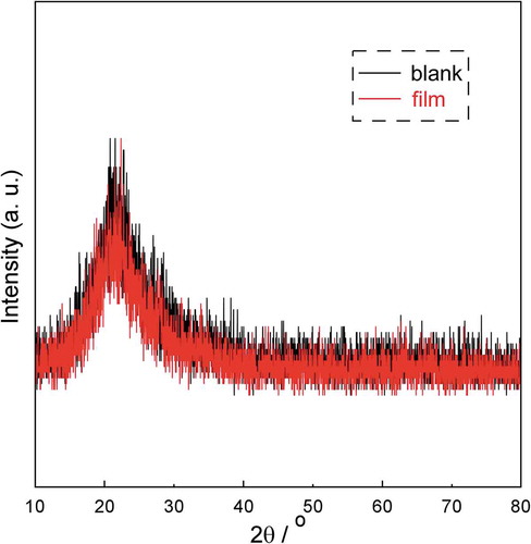
The XRD pattern of boron carbide thin film deposited at Tdep = 900°C, Ptot = 100 Pa is shown in . Boron carbide thin films obtained under various conditions exhibit a typical amorphous pattern with a broad peak around 22°C. The XRD patterns of the films prepared at distinct Tdep and Ptot are almost the same.
Figure 1. XRD patterns of fused quartz substrate and the boron carbide film prepared at Tdep = 900°C, Ptot = 100 Pa.
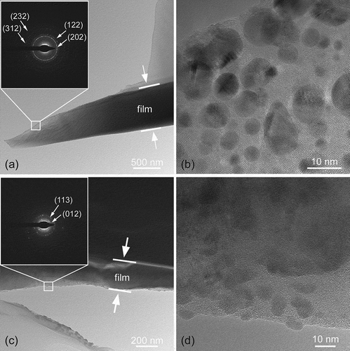
To further determine the structure of boron carbide films, transmission electron microscopy has been performed. Results obtained from TEM are present in . For film deposited at Tdep = 900°C and Ptot = 100 Pa, the diffraction rings are identified as the (202), (122), (312) and (232) planes of B4C. For film deposited at Tdep = 1200°C and Ptot = 50,000 Pa, diffraction rings of (012) and (113) planes of B4C appear, indicating that grains transformed when Tdep and Ptot increased. TEM results show that the structure of films is mainly amorphous boron carbide with dispersive B4C nano-grains. The average grain size was 7.3 nm and 9.2 nm, respectively, and the standard deviation of grain size was 2.69 nm and 1.5 nm, respectively [)]. This indicates that as Tdep and Ptot increased, the grains grow slightly and grain size becomes more uniform. In addition, the nano-grains of the film obtained at low Tdep and low Ptot are relatively dispersed, while the crystal grains of the film obtained at high Tdep and high Ptot seem to cluster.
Figure 2. Cross-section TEM images of boron carbide film prepared at (a) and (b) Tdep = 900°C, Ptot = 100 Pa; (c) and (d) Tdep = 1200°C, Ptot = 50,000 Pa.
The composition (as measured by XPS) of six samples is summarized in . Both carbon-rich film and boron-rich film were obtained. For films deposited at 900 oC and 1000 oC, carbon is the prominent element, with a B/C ratio in the range of 0.14–0.62. For films deposited at 1100 oC and 1200oC, boron is the prominent element, with a B/C ratio in the range of 1.30–3.29. This can indicate that C-C bond is easier to generate at relatively low temperature, while B-C bond and B-B bond generation consume more energy. Boron content is found to increase with increasing Tdep and Ptot, while carbon content is found to decrease. It is noticed that the B/C ratio is slightly affected by total pressure, whereas the deposition temperature has a strong effect on the B/C ratio in the films. It is reasonable to assume that the decomposition of precursor is temperature dependent, and at higher temperature more boron-containing molecule is formed [Citation21].
Table 2. CVD conditions and films elemental composition (as measured by XPS).
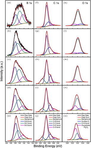
Chemical environment of the atoms in the deposited films was investigated using XPS analysis. Deconvoluted XPS spectra corresponding to B 1s and C 1s peaks of the deposited films are shown in . The B 1s spectra [–)] are fitted using three components assigned to B-B (188.0–188.4 eV), B-C (189.1–189.7 eV), and B-O (191.2–191.8 eV) [Citation13,Citation22,Citation23]. Dong et al. [Citation24], prepared boron carbide films by PECVD from ortho-carborane, divided B 1 s spectrum into three different B bonding environments: BCitation2-B at 188.4 eV, BC-B at 189.2 eV and C2-B at 189.9 eV, with relative intensities of 4:4:2. A possible explanation for such difference is that the orthocarborane icosahedron structure is no longer complete, due to higher deposition temperature by thermal CVD (900–1200°C) than by PECVD (50–450°C). In the case of B 1s spectrum, oxides occur at the highest binding energies around 191.5 eV is dominating in film deposited at low temperature and low Ptot [)], then reduced when temperature and Ptot increase [–)]. The peak appearing around 188.0 eV for all film matched well with the reported binding energy of B-B bonds. The component assigned to B-C bond centered at 189.4 eV is close to B-C binding energies for BC3.4.
Core level C 1s spectra [–)] has dominant peaks near 284.6 which corresponds to adventitious carbon (C-C), maybe due to films were stored exposing to ambient conditions [Citation25]. Compared with C 1s spectra of Dong et al. [Citation24], which shows a major peak at 283.8 eV, the C 1s binding energy in this study is a little bit higher. This also indicates that the icosahedral structure of ortho-carborane is no longer complete. Peaks appearing on the higher binding energies around 286.2 eV and 288 eV correspond to C = C and C-O bonds, respectively, [Citation26,Citation27]. Peaks observed near 283 eV correspond to C-B bond is inferior in film deposited at low temperature [,g)], then increases with increasing boron content [–)] [Citation13].
Figure 3. Effect of Ptot on elemental composition and B/C ratio of boron carbide film prepared at Tdep = 900°C.
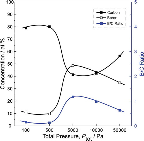
Figure 4. XPS spectra of B 1s (a–e), C 1s (f–j) and O 1s (k–o) for boron carbide film deposited at Tdep = 900°C, Ptot = 100 Pa (a), (f) and (k), Tdep = 1000°C, Ptot = 500 Pa (b), (g) and (l), Tdep = 1100°C, Ptot = 5000 Pa (c), (h) and (m), Tdep = 1200°C, Ptot = 10,000 Pa (d), (i) and (n), Tdep = 1200°C, Ptot = 50,000 Pa (e), (j) and (o).
O 1s spectra can be divided into three peaks: oxyboron carbide or B2O3 phases at 533 eV, C = O in oxides at 532 eV and surface chemisorbed oxygen at 531 eV [Citation22,Citation28]. At low Tdep and Ptot, oxygen mainly exists in the form of C = O, as Tdep and Ptot increases, oxygen is converted to oxyboron carbide or B2O3 phases. Compared with O1s spectra of Bute et al. [Citation22], which shows a dominant peak of surface oxygen, the oxygen in the films in this study may be due to residual oxygen inside the reactor.
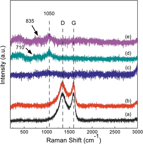
Raman spectra of the deposited boron carbide films in the spectral range 200 cm−1 to 3000 cm−1 are shown in . The dissimilarity of Raman bands reveals the different microstructure and phase composition of the coatings. The multiple Raman bands ranging from 700 cm−1 to 900 cm−1 have been assigned to the intraicosahedral or intericosahedral B–B bonds [Citation29]. The peak at 1050 cm−1 corresponds to the breathing modes of the icosahedral B11C structure [Citation30]. The bands at 1350 cm−1 (D-band) and 1590 cm−1 (G-band) are attributed to the presence of free carbon in films [Citation31]. In addition, it points out that the carbon content in the coatings deposited at low Tdep and Ptot is higher than in that deposited at high Tdep and Ptot for the relatively strong D-band and G-band in the Raman spectroscopes, which is consistent with the results of XPS. In the published literature on boron carbide, there is little information about B-H or C-H bonding. Two bending modes at 1164 and 1192 cm−1 as symmetric B-H and asymmetric B-H in ammonia borane were observed by Kupenko et al. [Citation32]. However, these peaks could not be identified in this study due to high background intensity. Although the results of this study do not provide direct data for the identification of B-H or C-H bonding, the introduction of B and H atoms may be reflected in the relatively large fwhm of the D and G peaks.
Figure 5. Raman spectra of boron carbide film synthesized at (a) Tdep = 900°C, Ptot = 100 Pa (b) Tdep = 1000°C, Ptot = 500 Pa (c) Tdep = 1100°C, Ptot = 5000 Pa (d) Tdep = 1200°C, Ptot = 10,000 Pa (e) Tdep = 1200°C, Ptot = 50,000 Pa.
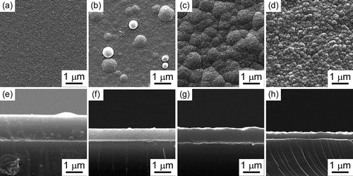
shows typical surface and cross-sectional morphologies of boron carbide films obtained at various Tdep and Ptot. The boron carbide film prepared at low temperature and low Ptot (Tdep = 900°C and Ptot = 100 Pa) showed a comparatively flat morphology [)]. Boron carbide film prepared at low temperature and high Ptot (Tdep = 900°C and Ptot = 50,000 Pa) appeared round bulges [)]. Boron carbide film prepared at high temperature and relatively low Ptot (Tdep = 1100°C and Ptot = 5000 Pa) exhibited a cauliflower-like surface [)]. Boron carbide film prepared at high temperature and high Ptot (Tdep = 1200°C and Ptot = 50,000 Pa) exhibited a uniform granular surface [)]. Cross-section SEM images [–)] show deposited films with thickness range 0.37–1.4 μm. It is observed that with an increase in deposition temperature and pressure, thickness of as deposited films decreased.
Figure 6. Surface and cross-section SEM images of boron carbide film prepared at Tdep = 900°C, Ptot = 100 Pa (a) and (e), Tdep = 900°C, Ptot = 50,000 Pa (b) and (f), Tdep = 1100°C, Ptot = 5000 Pa (c) and (g), Tdep = 1200°C, Ptot = 50,000 Pa (d) and (h).
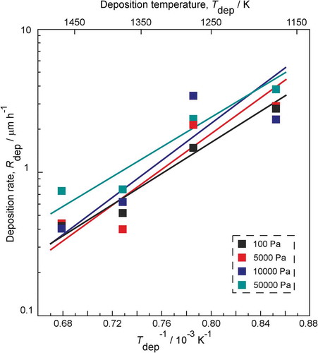
shows the relationship between the Rdep and the Tdep of boron carbide films at different Ptot. The Rdep ranged from 0.4 μm/h to 3.8 μm/h. The activation energy for these deposition processes was calculated to be −110 ± 10 kJ mol−1 in terms of Arrhenius equation. It indicates that the Rdep decreased with increasing Tdep at different Ptot. A probable explanation could be that increasing Tdep leads to higher re-sputtering rate during the deposition process; thus, Rdep is found to decrease [Citation22,Citation33].
Figure 7. Effect of Ptot and Tdep on the deposition rate of boron carbide films.
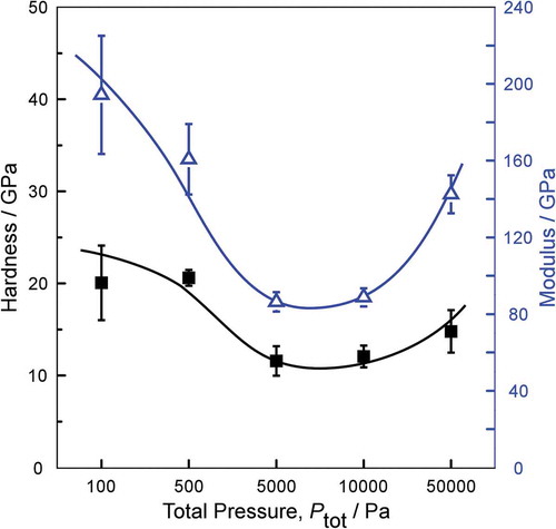
depicts the dependence of the hardness and modulus on Ptot for boron carbide film deposited at Tdep = 900°C. In order to exclude the effects of the substrates, the indentation depth of coatings should not exceed 10% of the film thickness, so the indentation depth of 100 nm was selected for films thickness is more than 1 μm. The performance correlates with the elemental composition of the films, which is shown in . With the increase of boron content, the hardness and modulus decrease. This is probably due to the presence of the amount of B-B bonding in the films, which may result in a less rigid structure because they do not form crosslinks in the network. The hardness of the (a-nc) boron carbide film obtained in this study reached 20.6 GPa, which was significantly improved compared with 8.1 GPa of a-BC film prepared by the Shahira et al. [Citation34]. The enhancement in mechanical properties may by cause of amorphous-nanocrystalline structure.
Figure 8. Effect of Ptot on hardness and modulus of boron carbide film prepared at Tdep = 900°C.
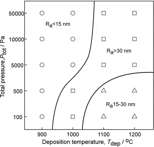
AFM images of boron carbide films deposited at four intense conditions are shown in . Surface roughness measurements, conducted on 5 × 5 μm regions, showed the surface roughness of the films deposited is 3.21, 9.18, 17.9 and 30.3 nm Rms, respectively. As shown in , the surface of the film is smooth when deposited at low Tdep and Ptot. With the increase of Tdep and Ptot, the roughness of the film increases and some round bulges appear on the surface. Trench with granular morphology can be observed in films deposited at high Tdep and Ptot. . Depicts the effects of Ptot and Tdep on the roughness of boron carbide films. Ra < 15 nm is considered as smooth, 15–30 nm for normal, and Ra >30 nm for rough. According to Ra, the samples can be divided into three regions. In the lower Tdep (900–1000°C) and higher Ptot (5000–50,000 Pa) region, films were smooth, which can also be seen from SEM images. With the increase of Tdep and Ptot, the roughness of films increases fast. It can be explained by an increase in grain size. In the high Tdep and Ptot region, the roughness of films drops lightly. An explanation could be that grain size is gradually uniform.
Figure 9. 3D AFM images of boron carbide film prepared at (a) Tdep = 900°C, Ptot = 100 Pa (b) Tdep = 900°C, Ptot = 50,000 Pa (c) Tdep = 1200°C, Ptot = 100 Pa (d) Tdep = 1200°C, Ptot = 50,000 Pa.
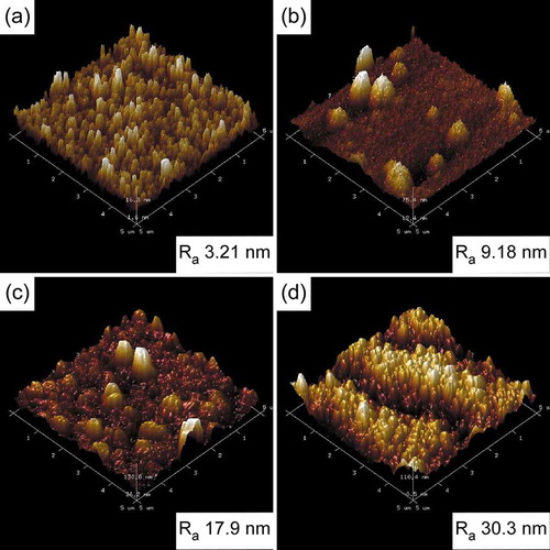
Figure 10. Effect of Ptot and Tdep on the roughness of boron carbide films.
4. Conclusions
Boron carbide films were prepared by thermal CVD using ortho-carborane (C2H12B10) as a single-source precursor. The B/C ratio of films is in the range of 0.14–3.29, which is increased with Tdep and Ptot increasing. Both carbon-rich films and boron-rich films were deposited, demonstrates that it is possible to prepare a film with preferred elemental composition, choosing appropriate deposition conditions. The TEM results show that the structure of the film is mainly composed of amorphous boron carbide with dispersive nano-grains, which will be able to improve the mechanical properties of the film with relatively low roughness. XPS analysis shows that the films contain mainly C-C, B-C and B-B bonds and to lower extent B-O as well as C-O bonds. B-O bonds were mainly found in films deposited at low temperature and low Ptot, while observed C-C bonds are primarily attributed to the formation of amorphous carbon phases in the films. Raman spectroscopy shows higher carbon content in films deposited at low temperature and Ptot for relatively strong D-band and G-band. This work points to the possibility to deposit (a-nc) boron carbide films through thermal CVD by using organoborane as a precursor. Moreover, this work can also provide references for CVD to fabricate amorphous/nanocrystalline compounds.
Disclosure statement
No potential conflict of interest was reported by the authors.
Additional information
Funding
References
- Ulrich S, Ehrhardt H, Samlenski R, et al. Subplantation effect in magnetron sputtered superhard boron carbide thin films. Diam Relat Mater. 1998;7:835–838.
- Sezer AO, Brand JI. Chemical vapor deposition of boron carbide. Mater Sci Eng B. 2001;79:191–202.
- Caruso AN, Dowben PA, Balkir S, et al. The all boron carbide diode neutron detector: comparison with theory. Mater Sci Eng B. 2006;135:129–133.
- Hong N, Crow L, Adenwalla S. Nuclear instruments and methods in physics research a time-of-flight neutron detection using PECVD grown boron carbide diode detector. Nucl Inst Methods Phys Res A. 2013;708:19–23.
- Höglund C, Birch J, Andersen K, et al. B4C thin films for neutron detection. J Appl Phys. 2012;111(104908):1–9.
- Mishra P, Ghosh SK, Srivastava C, et al. Synthesis and characterization of semiconducting BC films for neutron sensors by pulse DC plasma CVD. AIP Conf Proc. 2012;1451(118):117–120.
- Bradley SK, Nordell J, Karki S 1, et al. The influence of hydrogen on the chemical, mechanical,optical/electronic,and electrical transport properties of amorphous hydrogenated boron carbide. J Appl Phys. 2015;118(35703):1–17.
- Eroǧlu ÖD, Sezgi NA, Özbelge HÖ, et al. Synthesis and characterization of boron carbide films by plasma-enhanced chemical vapor deposition. Chem Eng Commun. 2003;190(3):360–372.
- Chaudhari P, Singh A, Topkar A, et al. Hot wire chemical vapor deposited boron carbide thin film/crystalline silicon diode for neutron detection application. Solid State Electron. 2012;78:156–158.
- Byun D. Comparison of different chemical vapor deposition methodologies for the fabrication of heterojunction boron-carbide diodes. NanoStruct Mater. 1995;5(4):465–471.
- Oliveira JC, Oliveira MN. Structural characterisation of B4C films deposited by laser-assisted CVD. Surf Coat Technol. 1996;80:100–104.
- Mustafa Karaman TD, Önder Özbelge H, Aslı Sezgi N. Mechanism and characterization studies on boron carbides deposited by chemical vapor deposition technique. Mater Res Soc. 2006;886:1–6.
- Imam M, Höglund C, Jensen J, et al. Trimethylboron as single-source precursor for boron-carbon thin film synthesis by plasma chemical vapor deposition. J Phys Chem C. 2016;120:21990–21997.
- Chen R, Su L, Qi J, et al. Effect of deposition time on the growth mode and stoichiometric of amorphous boron carbide thin films deposited by electron beam evaporation. Ceram Int. 2018;44(14):17298–17304.
- Jansson U, Carlsson JO. Chemical vapour deposition of boron carbides: phase and chemical composition. Thin Solid Films. 1989;172:81–93.
- Conde O, Silvestre AJ, Oliveira JC. Influence of carbon content on the crystallographic structure of boron carbide films. Surf Coat Technol. 2000;125:141–146.
- Lee S, Mazurowski J, Ramseyer G, et al. Characterization of boron carbide thin films fabricated by plasma enhanced chemical vapor deposition from boranes vapor deposition from boranes. J Appl Phys. 1992;72:4924–4933.
- Nordell BJ, Karki S. The influence of hydrogen on the chemical, mechanical, optical/ electronic,and electrical transport properties of amorphous hydrogenated boron carbide. Appl Phys. 2015;118:35703.
- Zhou S, Xue Q. The structure and tribological properties of aluminum/carbon nanocomposite thin films synthesized by reactive magnetron sputtering. Surf Interface Anal. 2011;43:1057–1063.
- Kilkenny JD, Glendinning SG, Haan SW, et al. A review of the ablative stabilization of the Rayleigh-Taylor instability in regimes relevant to inertial confinement fusion. Phys Plasmas. 1994;1(5):1379–1389.
- Henrik Pedersen AH, Hoglund C, Birch J, et al. Low temperature CVD of thin, amorphous boron-carbon films for neutron detectors. Chem Vap Depos. 2012;18:221–224.
- Bute A, Kar JR, Chopad S. Effect of self-bias on the elemental composition and neutron absorption of boron carbide films deposited by RF plasma enhanced CVD. Mater Chem Phys. 2016;182:62–71.
- Zeng B, Feng Z, Li S, et al. Microstructure and deposition mechanism of CVD amorphous boron carbide coatings deposited on SiC substrates at low temperature. Ceram Int. 2009;35:1877–1882.
- Dong B, Oyelade A, Kelber JA. Carborane-based polymers : a novel class of semiconductors with tunable properties. Phys Chem Chem Phys. 2017;19:10986–10997.
- Zhang S, Lu W, Wang C, et al. Stoichiometric controlling of pulsed laser deposited boron-carbon thin film. Phys B Phys Condens Matter. 2012;407(13):2382–2384.
- Li Q, Zhang S, Wang C, et al. Structural evolution of B-C thin films deposited from SPSed-target and dual-target. Am Ceram Soc. 2014;1370:1367–1370.
- Zhang S, Lu W, Wang C, et al. Stoichiometric controlling of boron carbide thin films by using boron-carbon dual targets. Appl Phys Lett. 2012;141602(101):9–13.
- Jacobsohn LG, Schulze RK, Maia MEH, et al. X-ray photoelectron spectroscopy investigation of boron carbide films deposited by sputtering. Surf Sci. 2004;572:418–424.
- Liu Y, Zhang L, Cheng L, et al. Uniform design and regression analysis of LPCVD boron carbide from BCl3-CH4-H2 system. Appl Surf Sci. 2009;255:5729–5735.
- Pallier C, Chollon G, Weisbecker P, et al. Structural changes of CVD Si-B-C coatings under thermal annealing. Surf Coat Technol. 2013;215:178–185.
- Wang C, Yang Y, Chung YW, et al. Microstructure, hardness and toughness of boron magnetron sputtering. Ceram Int. 2016;42(5):17298–17304.
- Kupenko I, Dubrovinsky L, Dmitriev V, et al. In situ Raman spectroscopic study of the pressure induced structural changes in ammonia borane. J Chem Phys. 2012;74506:1–9.
- Robertson J. Diamond-like amorphous carbon. Mater Sci Eng. 2002;37:129–281.
- Liza S, Ohtake N, Akasaka H, et al. Tribological and thermal stability study of nanoporous amorphous boron carbide films prepared by pulsed plasma chemical vapor deposition. Sci Technol Adv Mater. 2015;16(35007):1–13.