
 ?Mathematical formulae have been encoded as MathML and are displayed in this HTML version using MathJax in order to improve their display. Uncheck the box to turn MathJax off. This feature requires Javascript. Click on a formula to zoom.
ABSTRACT
Ceramics of composition 0.75(Na1/2Bi1/2)TiO3-0.25SrTiO3 (NBT-25ST) show a giant electric field-induced strain, making them attractive for actuator applications. Single crystals generally have improved piezoelectric properties over their ceramic counterparts, but the electrical properties of NBT-25ST single crystals have not yet been studied. In this work, NBT-25ST single crystals are grown by the solid state crystal growth technique and their electrical properties measured for the first time. The single crystals show relaxor ferroelectric behavior typical of an NBT-type material. The ferroelectric and inverse piezoelectric properties depend strongly on crystallographic orientation, with superior properties in the (001) orientation. The inverse piezoelectric properties of the (001)-oriented NBT-25ST single crystal are superior to those of an NBT-25ST ceramic (Smax/Emax = 1042 pm/V vs. 739 pm/V).
1. Introduction
Piezoactuators have been applied in many areas such as electric fuel injection, autofocusing of cameras, ink-jet printers, optical lenses and mirrors [Citation1,Citation2]. A piezoactuator can be designed based on physical dimensions, displacement (stroke), blocking force, maximum strain, temperature range, frequency range and voltage range [Citation2,Citation3]. Piezoactuators must operate in many different environments and are affected by many factors such as temperature, frequency, pressure and humidity [Citation3–5]. At the present time, the global market for piezoactuators is dominated by Lead Zirconate Titanate (PZT), which has excellent piezoelectric properties such as Smax/Emax ≈ 700 pm/V, ε33T/ε0 = 2300, Tc = 250°C [Citation2,Citation6–8]. However, the high concentration of lead in PZT can negatively affect human health and the environment [Citation2]. To mitigate these effects, restrictions on the amount of lead permissible in electronic devices have been applied through the RoHS and WEEE regulations from the European Union and similar legislation from various countries [Citation2,Citation7,Citation9]. Therefore, the discovery of new lead-free materials with piezoelectric properties that are comparable to PZT is urgently required. Many efforts from researchers to look for and discover new material systems have been in progress. Many methods were proposed to improve the piezoelectric properties of well-known lead-free systems by making binary or ternary solid solutions, doping or fabrication of single crystals [Citation2,Citation3,Citation10–21].
Sodium Bismuth Titanate, (Na1/2Bi1/2)TiO3 (NBT), is a relaxor ferroelectric material with high coercive electric field that makes it difficult to pole [Citation2,Citation22]. Below 255°C, NBT is rhombohedral. The space group is generally considered to be R3c [Citation23,Citation24], although a monoclinic structure (space group Cc) is also possible [Citation25]. Rhombohedral to tetragonal (P4bm) and tetragonal to cubic phase transitions take place at ~255°C and ~540°C respectively [Citation24,Citation26–28]. The rhombohedral and tetragonal phases co-exist between 255–400°C, while the tetragonal and cubic phases co-exist between 500–540°C [Citation24]. To improve the electrical properties, SrTiO3 (ST) was combined with NBT; the Sr2+ ion is dispersed in the NBT crystal lattice to make a solid solution [Citation11,Citation29]. The coercive electric field is decreased, which assists poling [Citation30]. Addition of ST to NBT causes the NBT rhombohedral structure to change to a pseudocubic structure as ST concentration increases, with a morphotropic phase boundary (MPB) existing between rhombohedral and pseudocubic phases at x ≈ 0.25 [Citation11,Citation31,Citation32]. At compositions near the MPB the piezoelectric properties can be improved, at the cost of a reduction in the depolarization temperature Td and the rhombohedral to tetragonal phase transition temperature TR-T [Citation29–32]. Hiruma et al. studied the (100-x)NBT-xST system and found that compositions near the MPB with x = 26–28 mol % had improved inverse piezoelectric properties with a strain of 0.29% and a normalized strain Smax/Emax of 488 pm/V [Citation11]. Acosta et al. found that 75 mol % (Na1/2Bi1/2)TiO3 – 25 mol % SrTiO3 (NBT-25ST) ceramics, which have a composition close to the MPB, showed a normalized strain Smax/Emax of 600–700 pm/V at a relatively low electric field of 4 kV/mm [Citation3].
Single crystals of NBT-based compositions generally have improved properties relative to their ceramic counterparts [Citation33,Citation34]. Some NBT-BT single crystals with compositions near to the morphotropic phase boundary between rhombohedral and tetragonal phases exhibit a high Smax/Emax and free strain such as 0.945(Na1/2Bi1/2)TiO3-0.055BaTiO3, with Smax/Emax ≈ 1420 pm/V and 0.44% strain, and Na1/2Bi1/2TiO3-Ba(Ti,Zr)O3, with Smax/Emax ≈ 2000 pm/V and 0.45% strain [Citation35–37]. Single crystals of (Na1/2Bi1/2)TiO3-BaTiO3-(K0.5N0.5)NbO3 (NBT-BT-KNN) compositions showed a giant strain of 0.57% and Smax/Emax of 950 pm/V [Citation38] and a giant strain of 0.83% at an electric field of 28 kV/cm [Citation39]. Single crystals of NBT-25ST may also have improved piezoelectric properties, but as of yet only limited work on single crystal growth in this system has been reported and the electrical properties have not been measured [Citation13].
In the present work, the solid state crystal growth technique is used to grow single crystals [Citation40,Citation41]. In this technique, a piece of single crystal (the seed crystal) is buried inside the polycrystalline powder of the composition to be grown, pressed into a pellet and then sintered. A single crystal with the same composition as the powder grows epitaxially on the seed crystal. The relatively low processing temperature (lower than the melting point of the compound to be grown) helps the single crystal preserve its stoichiometry and chemical homogeneity. Solid state crystal growth has been used to grow single crystals with properties comparable to those of conventionally-grown crystals. Single crystals of (Na1/2Bi1/2)TiO3-BaTiO3, (Na1/2Bi1/2)TiO3-Ba(Ti,Zr)O3, (Na1/2Bi1/2)TiO3-CaTiO3, (Na1/2Bi1/2)TiO3-SrTiO3 and (Na1/2Bi1/2)TiO3-BaTiO3-(K0.5N0.5)NbO3 have been grown by this technique [Citation13,Citation15,Citation33,Citation38,Citation42–45]. In the present work, single crystals of 75 mol % (Na1/2Bi1/2)TiO3 – 25 mol % SrTiO3 (NBT-25ST) are grown by solid state crystal growth and the microstructure, structure and electrical properties of the grown single crystals are studied. Single crystals of NBT-25ST are found to have significantly improved inverse piezoelectric properties over their ceramic counterparts.
2. Experimental
The NBT-25ST powder is synthesized from Na2CO3 (ACROS organics, 99.5%), Bi2O3 (Alfa Aesar, 99.9%), TiO2 (Alfa Aesar, 99.8%) and SrCO3 (Aldrich, ≥ 99.9%) starting materials by solid state reaction. For further details, see reference [Citation13]. SrTiO3 single crystal seeds (MTI Corp., CA) with (110) orientation and dimensions of 5 mm × 5 mm × 0.5 mm are buried in 0.5 g of powder in a 10 mm steel die which is then pressed by hand into pellets, followed by cold isostatic pressing at 1500 kg.cm−2 (~ 147 MPa). The pellets are sintered at 1250°C for 5 h with heating and cooling rates of 5°C.min−1. To reduce volatilization of Na and Bi during sintering, the pellets are buried in a 2 wt% Na2CO3 – 2 wt% Bi2O3 – 96 wt% NBT-25ST packing powder in double alumina crucibles with lids. A schematic diagram of the experiment is shown in Figure S 1(a).
To study the microstructure, samples are vertically sectioned, polished to a 1 µm finish with diamond suspension and thermally etched at 1200°C for 1 h. The etched samples are Pt-coated and observed by Scanning Electron Microscopy (SEM, Hitachi S-4700, Tokyo, Japan) with attached Energy Dispersive X-ray spectrometer (EDS, EMAX energy EX-200, Horiba, Kyoto, Japan). The mean matrix grain size and matrix grain size distribution are analyzed from the SEM micrographs using imageJ v1.50a image analysis software (National Institute of Mental Health, Bethesda, MD). To analyze the mean matrix grain size and grain size distribution, the equivalent 2D radii of at least 200 grains are analyzed. For EDS analysis, a polished and un-etched sample was used.
To study the structure, a single crystal sample is polished with SiC paper up to grade #4000 to expose NBT-25ST single crystal faces with (110) orientation on both sides. The sample is analyzed by X-ray diffraction (XRD, X’Pert PRO, PANalytical, Almelo, the Netherlands) using CuKα radiation, a scan range of 20–90° 2θ and a scan speed of 3°C.min−1. Kα2 peak removal was carried out using MDI Jade 6.5 (Materials Data Inc., CA). For micro-Raman scattering, a single crystal sample is removed from the matrix and polished to a 1 µm finish with diamond suspension to expose the (110)-oriented NBT-25ST single crystal face on one side. To remove strains generated during polishing, the sample is annealed at 400°C for 1 h and cooled at a rate of 1°C.min−1. Micro-Raman scattering is carried out with a 514 nm Ar+ ion laser and output power of 10 mW (LabRam HR800 UV Raman microscope, Horiba Jobin-Yvon, France). The Raman spectrum is recorded at room temperature in back scattering geometry with a resolution of ~0.5 cm−1. The diameter of the laser spot on the sample is 1–2 μm. Peak fitting of Gaussian peaks is carried out using fityk 0.9.8 peak fitting software [Citation46].
To carry out impedance spectroscopy, the single crystal sample that had been prepared for XRD analysis is used. Both (110) faces of the single crystal are coated with Pt-paste and the sample is annealed at 900°C for 30 min with heating and cooling rates of 5°C.min−1 to prepare Pt electrodes. An impedance analyzer (HP4284A, Hewlett-Packard, Kobe, Japan) is used to record the electrical properties of the sample at different temperatures and frequencies. The sample is measured in a furnace in the temperature range of 30 to 800°C in oxygen with heating and cooling rates of 1°C.min−1. The AC voltage was set at 0.1 V and the frequency range from 1000 kHz to 39.8 Hz. For comparison, a ceramic NBT-25ST sample is prepared by sintering a 0.3 g pellet (without seed crystal) at 1250°C for 1 h, with heating and cooling rates of 5°C.min−1 and its electrical properties measured in the same way.
As will be seen, the single crystals of NBT-25ST grown by solid state crystal growth are limited in thickness. In order to prepare larger NBT-25ST single crystals for measurement of the inverse piezoelectric properties, top-seeded solid state crystal growth experiments are carried out [Citation47]. Details of these experiments, as well as details of the SEM and XRD analyses, are provided in the supplemental material. Single crystal samples with (110) and (001) major faces are prepared for electrical property measurements (Figure S 2). For polarization and strain hysteresis measurements, silver paste electrodes are applied on the (110) or (001) major faces of the samples. The external electric field (E) dependencies of polarization (P) and strain (S) hysteresis are measured in a commercial apparatus, aixPES (aixACCT system GmbH, Aachen, Germany) using a bipolar electric field profile at 1 Hz. To carry out impedance spectroscopy, Pt paste electrodes are applied as before. Samples are measured in the temperature range of 70 to 800°C in oxygen with heating and cooling rates of 1°C.min−1. The AC voltage was set at 1 V and the frequency range from 1000 kHz to 39.8 Hz.
3. Results
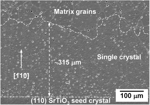
An SEM micrograph of a sample are shown in . An NBT-25ST single crystal has grown epitaxially on the SrTiO3 seed crystal. At a sintering temperature of 1250°C, a grown single crystal thickness of ~315 μm was obtained after sintering for 5 h. In the matrix, coarse grains are predominant (Figure S 3(a)). Porosity is visible in both the single crystal and the matrix grains. Micro-faceting of the grains is visible as steps on the grain boundaries. Some examples are marked with arrows in Figure S 3(a). The matrix grain size distribution shows that the matrix grains have a bimodal size distribution with the largest grain reaching to ~85 μm in radius as shown in Figure S 3(b). The mean size and standard deviation of the matrix grains is 21 ± 16 μm.
Figure 1. SEM micrograph of an NBT-25ST single crystal grown by solid state crystal growth
Energy Dispersive X-ray Spectroscopy (EDS) results are shown in . EDS was taken on ten points on the single crystal and ten points on the matrix grains. The results show the mean and standard deviation. The NBT-25ST single crystal is slightly deficient in Na and has an excess of Bi. The matrix grains show similar behavior but the Na loss is less pronounced and the Bi excess is slightly more pronounced.
Table 1. EDS analysis results of an NBT-25ST single crystal grown by solid state crystal growth and its surrounding matrix grains
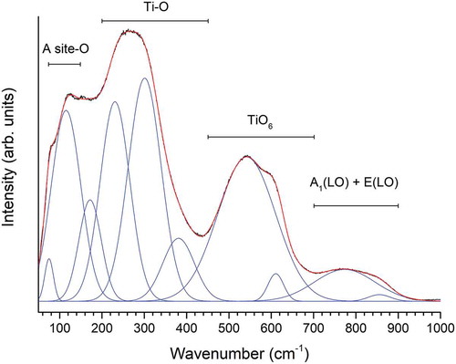
The NBT-25ST single crystal sample shows two peaks in the XRD pattern (), which can be indexed as 110 and 220 peaks using pseudocubic indices. The top and bottom faces of the single crystal sample show identical XRD patterns, showing that the sample is single crystalline throughout its thickness. An XRD pattern of a (110) oriented SrTiO3 single crystal substrate is also shown for comparison. The positions and d-spacings of the 110 peaks for the NBT-25ST and SrTiO3 single crystals are given in Table S1. The XRD results show that the NBT-25ST single crystal has epitaxially grown on the SrTiO3 seed crystal. However, the peak positions and lattice parameters of the substrate and grown single crystal are slightly different, so the grown single crystal has some mismatch with the seed crystal. A Raman spectrum of the NBT-25ST single crystal is shown in . The black curve is the experimental data, the blue curves are the fitted peaks and the red curve is the sum of the fitted peaks. Gaussian peaks were fitted as this peak shape is more suitable for fitting the spectra of solids [Citation48]. Wavenumber regions corresponding to the different types of vibrations (described in the Discussion) are indicated.
Figure 2. X-ray diffraction patterns of a single crystal NBT-25ST sample grown by solid state crystal growth and a SrTiO3 seed crystal
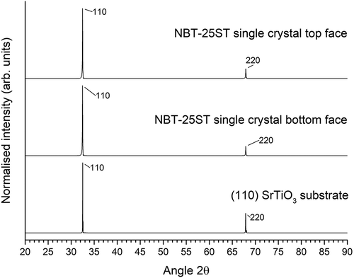
Figure 3. Raman spectrum of an NBT-25ST single crystal grown by solid state crystal growth. The black curve is the experimental data, the blue curves are the fitted Gaussian peaks and the red curve is the sum of the fitted peaks. Wavenumber regions corresponding to the different types of vibrations are indicated
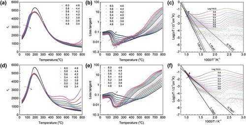
The impedance spectroscopy results of the NBT-25ST single crystal and polycrystalline samples are presented in . The numbers in the legends are the logarithmic values of the measurement frequency. The curved arrows show the directions of increasing measurement frequency. The plots of the real part of the relative permittivity ε’r vs. temperature show broad peaks with a maximum at ~ 190°C (). At temperatures below the peak temperature, the value of ε’r decreases as measurement frequency increases. At temperatures close to and above the peak temperature, ε’r does not show much dispersion with frequency. A shoulder is visible in the ε’r vs. temperature curves of the single crystal sample at ~135°C. A corresponding shoulder is hardly visible in the polycrystalline sample. In the curves for the polycrystalline sample, peaks are visible at temperatures > 500°C, becoming smaller as measurement frequency increases. These peaks are due to polarization effects at the electrodes. In the plots of loss tangent vs. temperature, peaks corresponding to the ε’r shoulder at ~135°C are clearly visible, both in the single crystal and polycrystalline samples (). The peaks move to higher temperature and larger value of loss tangent with increasing measurement frequency. Loss tangent minima, corresponding to the peaks in ε’r, are visible at lower measurement frequencies. The low frequency data for ε’r and loss tangent are not shown as it is very noisy. As previously reported [Citation15,Citation43,Citation49–51], from the AC conductivity curves (), activation energies of 1.65 eV and 1.19 eV above ~600°C at the low frequency limit can be estimated for the single crystal and polycrystalline samples respectively (calculated from the data measured at 39.8 Hz) [Citation52,Citation53].
Figure 4. Real part of the relative permittivity, loss tangent and conductivity as functions of temperature measured in the temperature range from 30 to 800°C on (a) – (c) an NBT-25ST single crystal grown by solid state crystal growth and (d) – (f) an NBT-25ST polycrystalline sample. The numbers in the legends are the logarithmic values of the measurement frequency
An SEM micrograph of an NBT-25ST single crystal grown by top-seeded solid state crystal growth is shown in . A single crystal of NBT-25ST has grown ~1,200 μm in the [110] direction. The interfacial region between the single crystal and the matrix grains is shown in Figure S 4(a). A secondary phase can be seen at the matrix grain boundaries and in the single crystal. EDS analysis of the secondary phase in the matrix shows it to be TiO2. The secondary phase in the single crystal may be an artifact caused by thermal etching [Citation15,Citation42]. The matrix grain size distribution of this sample is shown in Figure S 4(b). The mean and standard deviation of the matrix grain size is 14 ± 6 μm. EDS analysis results are shown in . Each value is the mean and standard deviation of five measurement points. Both the single crystal and the matrix grains have excess Na and Bi compared to the nominal values.
Table 2. EDS analysis results of an NBT-25ST single crystal grown by top seeded solid state crystal growth and its surrounding matrix grains
Figure 5. SEM micrograph of an NBT-25ST single crystal grown by top-seeded solid state crystal growth
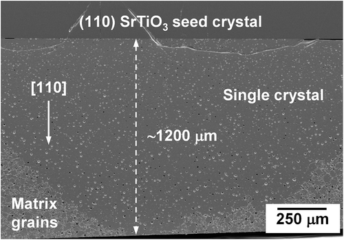
Figure S 2(a) shows the NBT-25ST single crystals oriented in the [100] and [110] directions with their dimensions. Figure S 2(b) shows XRD patterns of the single crystals. The peaks are again indexed using pseudocubic indices. The peaks of the (001)-oriented single crystal show shoulders on the low angle side. These may be caused by a skin layer on the sample [Citation54]. The Rietveld refinement results of the annealed powder sample prepared from a polycrystalline NBT-25ST ceramic are given in Table S2. Refinement was carried out using rhombohedral (R3c), tetragonal (P4bm), cubic and coexisting rhombohedral + tetragonal, rhombohedral + cubic and tetragonal + cubic phases. Coexisting rhombohedral and cubic phases provide the best fit to the data. The XRD pattern, Rietveld refinement and difference plot of the annealed polycrystalline NBT-25ST powder sample is shown in Figure S 5. The pattern was fitted with coexisting rhombohedral (R3c) and cubic
phases. The sample contains ~76 vol. % rhombohedral phase and ~24 vol. % cubic phase.
The polarization-electric field (PE) and bipolar strain-electric field (SE) hysteresis loops of the (001)- and (110)-oriented NBT-25ST single crystal samples are shown in . For comparison, polarization and strain hysteresis curves of a polycrystalline sample (sintered at 1250°C for 1 h) are also shown. The properties of the samples are given in . The (001)-oriented NBT-25ST single crystal sample has a narrow, pinched PE loop and a sprout-shaped SE bipolar loop with almost zero remanent and negative strain (). The polycrystalline NBT-25ST sample also has a narrow, pinched PE loop and a sprout-shaped SE bipolar loop (). The properties of the polycrystalline NBT-25ST sample are comparable to those previously measured [Citation3,Citation11]. Compared with the polycrystalline sample, the (001)-oriented single crystal shows lower coercivity Ec, increased saturation polarization Ps, remnant polarization Pr and maximum strain Smax, an increase in Smax/Emax of 41% and a reduced strain hysteresis ΔS/Smax of 18%, where ΔS is the difference in strain between the upper and lower parts of the curve when E = maximum electric field Emax/2 [Citation38]. The Smax/Emax value of the (001)-oriented NBT-25ST single crystal sample is comparable to those of (Na1/2Bi1/2)TiO3-BaTiO3-(K0.5N0.5)NbO3 single crystals [Citation38,Citation44].
Table 3. Ferroelectric and piezoelectric properties of (001)- and (110)-oriented NBT-25ST single crystals grown by top-seeded solid state crystal growth and a polycrystalline sample
Figure 6. Polarization vs. electric field and strain vs. electric field hysteresis loops of NBT-25ST single crystals grown by top-seeded solid state growth: (a, b) (001) orientation; (c, d) (110) orientation; (e, f) NBT-25ST polycrystalline sample
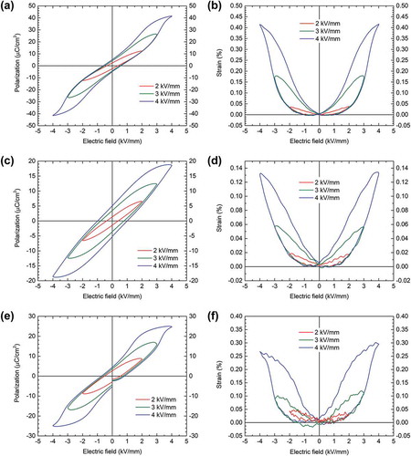
The behavior of the (110)-oriented NBT-25ST single crystal is quite different (). The PE hysteresis loops are slim but do not have a pinched appearance. The PE loops are also not well saturated with relatively low Ps. The bipolar SE loops are also slim with almost zero remnant and negative strain, but the shape is slightly different to that of the (001)-oriented NBT-25ST single crystal and also that of the polycrystalline sample. Smax is also greatly reduced.
The impedance spectroscopy results of the (001) and (110)-oriented NBT-25ST single crystals are presented in Figure S 6. The results appear similar to those in . However, the temperature of maximum ε’r increases to ~215°C and the values of loss tangent in the temperature range 400–600°C are larger than those of the single crystal in . The plots of ε’r vs. temperature for both orientations have a shoulder at ~135°C. The values of ε’r for the (001)-oriented single crystal are larger than those of the (110)-oriented single crystal. In the plots of loss tangent vs. temperature, the drop in loss tangent corresponding to the shoulder in ε’r is more clearly defined for the (001)-oriented sample.
4. Discussion
In the solid state crystal growth technique, the seed crystal acts as a rapidly growing abnormal grain and consumes the surrounding matrix grains, causing a single crystal of the matrix composition to grow epitaxially onto the seed [Citation41,Citation55]. For single crystal growth to take place, the grain boundaries must be ordered [Citation41,Citation56], as was found in previous work on NBT-based ceramics [Citation13,Citation57,Citation58] and as indicated by the presence of micro-facets at the grain boundaries (Figure S 3(a)) [Citation59]. The broad matrix grain size distribution (Figure S 3(b)) shows that abnormal grain growth has occurred, where abnormal grains are defined as grains with a radius greater than three times the mean grain radius [Citation58].
As the single crystal’s driving force for growth decreases as mean matrix grain size increases [Citation41], retarding grain growth in the matrix (especially abnormal grain growth) is important in order to grow a large crystal. The NBT-25ST system suffers from abnormal grain growth, as can be seen in Figure S 3, which restricts growth of the single crystal. In the single crystals grown by top-seeded solid state crystal growth, the single crystal growth distance is larger and the matrix grains are smaller than in the sample grown by solid state crystal growth ( and Figure S 4(a)). Also, the grain size distribution is narrower (Figure S 4(b)). During the pre-sintering step at 900°C some matrix grain growth will take place. This will lower the driving force for growth of the matrix grains in the subsequent annealing step at 1250°C [Citation60], reducing their growth rate and delaying the onset of abnormal grain growth. The smaller matrix grain size means an increased driving force for single crystal growth, leading to increased single crystal growth. The EDS results also show the matrix grains in the sample grown by top-seeded solid state crystal growth to be slightly more Bi-excess (), which may also affect the growth behavior. Bi-excess was found to reduce grain growth in NBT [Citation61].
From the EDS results (), it is seen that the single crystals grown by solid state crystal growth at 1250°C for 5 h are Na-deficient due to volatilization of Na2O during sintering, as also found in our previous work [Citation13]. Compared to the previous work, which used a packing powder without excess Na2CO3 and Bi2O3, the use of a packing powder with excess Na2CO3 in the present work could reduce the amount of Na volatilization. From the EDS results of the single crystal grown by top-seeded solid state crystal growth (), it appears that surrounding the sample with compacted NBT-25ST powder and NBT-25ST packing powder is effective in preventing Na and Bi losses by evaporation.
Raman spectra of NBT-based materials are generally separated into three regions. Modes between 100–150 cm−1 are associated with A1-symmetry Na-O vibrations or vibrations of other A-site cations [Citation29,Citation62]. The mode at ~75 cm −1 may correspond to Bi-O vibrations [Citation63]. Modes at 200–450 cm−1 are associated with A1-symmetry Ti-O vibrations, while modes in the region 450–700 cm−1 are associated with vibrations of the TiO6 octahedra [Citation29]. A1(LO) and E(LO) overlapping bands are probably the cause of modes in the region between 700–900 cm−1 [Citation64]. The shapes of the peaks in the different spectral regions are sensitive to the phase or phases present in the material [Citation63,Citation65–67]. For rhombohedral NBT, the peak at ~270 cm−1 is relatively narrow and can often be fitted with a single mode. The peaks in the region 450–700 cm−1 are merged together and are not well defined. For tetragonal NBT, the peak at ~270 cm−1 becomes broader and may be fitted with two modes [Citation65–68]. A shoulder on the high wavenumber side may appear. The peaks in the region 450–700 cm−1 begin to separate and become more clearly defined. The Raman spectrum of the NBT-25ST single crystal is in an intermediate state (). The peak at ~270 cm−1 is broad enough to be fitted with two modes, but the shoulder at the high wavenumber side has not appeared. Likewise the peaks in the region 450–700 cm−1 are beginning to separate. The overall appearance of the spectrum is similar to that of (Na1/2Bi1/2)TiO3-BaTiO3 ceramics in the MPB region between rhombohedral and tetragonal phases [Citation63,Citation65–67], indicating that the NBT-25ST single crystal contains both rhombohedral and tetragonal regions.
From the XRD and Rietveld refinement results (Figure S 5 and Table S2), the NBT-25ST structure appears to consist of coexisting rhombohedral and cubic phases. The fact that the NBT-25ST structure in the present work is not perfectly cubic is also evident from the presence of remanent polarization (). This is consistent with the study or Rout et al., which found an MPB between rhombohedral and pseudocubic (tetragonal) phases at x ≈ 0.25 [Citation29]. Likewise, Sayyed et al. found an MPB between rhombohedral and pseudocubic phases at x = 0.25–0.26 [Citation32]. However, Tong et al. found that their 0.74(Na1/2Bi1/2)TiO3-0.26SrTiO3 ceramics contained coexisting pseudocubic and tetragonal phases [Citation69]. The present work also differs from previous work on the 0.75(Na1/2Bi1/2)TiO3-0.25SrTiO3 composition by Acosta et al., in which a pseudocubic structure was reported [Citation3]. It is difficult to determine the structure of NBT-based materials using XRD, as the rhombohedral and tetragonal distortions are very small and the average structure often appears cubic [Citation70,Citation71]. This may explain why the XRD results indicate coexisting rhombohedral and cubic phases whereas the Raman scattering results indicate coexisting rhombohedral and tetragonal phases. The NBT-25ST structure may contain a tetragonal phase whose correlation length is too short to be detected by XRD, but which can be detected at the unit cell level by Raman scattering [Citation72]. The reduction in the rhombohedral to tetragonal phase transition temperature TR-T toward room temperature with increasing SrTiO3 concentration may also account for the presence of a tetragonal phase [Citation11]. Further study on the phase composition of this material needs to be carried out to account for the conflicting experimental results of different authors.
The plots of ε’r and loss tangent vs. temperature () are similar to those measured by previous workers on this composition and show behavior typical of NBT relaxor ferroelectric materials [Citation3,Citation30,Citation73]. The broad peaks with a maximum at ~ 190°C do not correspond to the Curie temperature but are associated with the thermal evolution of polar nanoregions [Citation74,Citation75] or a transition between polar and nonpolar tetragonal phases [Citation76]. The nature of the shoulders at ~135°C is not yet certain. They may correspond to the transition from the rhombohedral phase to the mixed rhombohedral and tetragonal phases [Citation24,Citation77–79], thermal evolution of mixed rhombohedral and tetragonal polar nanoregions [Citation75], a transition from a non-ergodic to ergodic relaxor [Citation80] or from a ferroelectric to relaxor state [Citation74]. The plots of ε’r and loss tangent vs. temperature of the single crystals prepared by top-seeded solid state crystal growth show differences in behavior to those of the single crystal prepared by solid state crystal growth. These differences may be due to the different sample preparation conditions leading to differences in composition ( and 2) [Citation61,Citation81]. The ε’r values of the single crystals vary with crystallographic orientation (Figure S 6). A similar variation in values of relative permittivity with crystallographic orientation has also been found in single crystals of NBT-BaTiO3 [Citation82,Citation83].
The activation energy values of 1.65 eV and 1.19 eV estimated from the AC conductivity curves () are considered to represent the electronic conductivity. The activation energy of 1.65 eV observed for the single crystal sample appears to be close to half of the band gap value of NBT-based materials [Citation84–86]. The smaller activation energy of 1.19 eV and high conductivity values observed in the polycrystalline sample may be ascribed to the extrinsic effects induced by the presence of the grain boundaries, e.g. facilitated oxidation/reduction reactions. It is notable that the AC conductivity plots of the polycrystalline sample indicate another Arrhenius behavior of activation energy ~ 0.70 eV. As the high temperature extrapolation of this lower activation energy trace does not determine the high temperature conductivity behavior, the feature could not be explained by the brick-layer model in the presence of blocking grain boundaries. Therefore it is suggested that the trace of activation energy 0.70 eV may represent the ionic conduction mechanism in perovskites. Oxide ion conductivity or alkali ion conductivity has been discussed to explain high DC loss and electrode polarization in ferroelectric perovskites but few conclusive investigations have been reported yet [Citation52,Citation53,Citation87–89]. It is notable that the traces of activation energies of 1.19 eV and 0.70 eV are also indicated in the single crystal sample in (the thin black lines), in addition to a trace (the dashed line) of a line parallel to that of the 1.65 eV trace for the DC limit conductivity. This trace has conductivity values about 2.3 times higher than the DC limit conductivity, similar to the current constriction effects due to the grain boundaries of ionic conductors [Citation90–92]. The origin of such current constriction effects in a nominally single crystalline sample should also be understood in future work together with the other traces related to the mixed conduction effects.
The narrow, pinched PE loops and sprout-shaped SE bipolar loops of the (001)-oriented NBT-25ST single crystal sample () and polycrystalline sample () are characteristic of an electric-field induced transformation from an ergodic relaxor phase to a ferroelectric phase [Citation3,Citation7,Citation70,Citation75,Citation79,Citation93–95]. The difference in shape of the PE and SE loops of the (110)-oriented NBT-25ST single crystal sample () shows that the ferroelectric and inverse piezoelectric behavior of NBT-25ST depends on the crystallographic orientation. The PE loops of the (110)-oriented NBT-25ST single crystal sample also appear unsaturated, possibly due to the low value of the applied electric field. The NBT-25ST single crystals have relatively high conductivity, which makes applying higher electric fields difficult.
Similar variation of piezoelectric properties with crystallographic orientation has been found in other NBT-based single crystals [Citation44,Citation79,Citation82,Citation83,Citation96,Citation97] and is generally the case for single crystals e.g. BaTiO3 [Citation98], KNbO3 [Citation99,Citation100] and relaxor-PbTiO3 [Citation101,Citation102]. This dependence of piezoelectric properties on crystallographic orientation is due to the different types of ferroelectric domain structure that form during poling (domain engineering) [Citation82,Citation83,Citation102], different electric field induced phase transitions [Citation103–105], polarization extension [Citation79,Citation106] and polarization rotation [Citation106] (although polarization rotation does not take place in NBT-based materials [Citation79]). For NBT-based compositions, application of an electric field along different crystallographic directions causes different electric field induced phase transitions to take place. Luo et al. studied the behavior of (Na1/2Bi1/2)TiO3-5.6% BaTiO3 single crystals under electric fields applied along the pseudocubic [001] and [111] directions using XRD and unipolar strain hysteresis measurements [Citation95]. At temperatures close to Td, application of an electric field along [001] caused a phase transition from pseudocubic to tetragonal phases with a large strain. Application of an electric field along [111] caused a pseudocubic – rhombohedral phase transition with a lower resultant strain. Chen et al. used electric field-dependant Raman scattering and XRD to study the orientation-dependant behavior in single crystals of 0.92(Na1/2Bi1/2)TiO3–0.06BaTiO3–0.02(K0.5Na0.5)NbO3 [Citation97]. They found that their (001)-oriented single crystal underwent an electric-field induced pseudocubic to tetragonal phase transition with a large resultant strain, whereas their (111)-oriented single crystal underwent a partial pseudocubic to rhombohedral phase transition with a small resultant strain. Similar behavior may also be happening in the NBT-25ST single crystals in the present work. This could also explain the increase in strain for the NBT-25ST single crystal sample oriented in the [001] direction compared to the polycrystalline sample at electric fields of ≥3 kV/mm. The single crystal can be oriented with its [001] direction parallel to the electric field, thus maximizing the electric-field induced pseudocubic to tetragonal phase transition. The polycrystalline ceramic will have grains randomly oriented to the electric field, limiting the degree of pseudocubic to tetragonal phase transition that can take place [Citation79]. The NBT-25ST single crystals have inverse piezoelectric properties superior than those of PZT i.e. Smax/Emax ≈ 625–750 pm/V for a soft PZT at an electric field of 4 kV/mm vs. 1042 pm/V for the NBT-25ST single crystal [Citation2,Citation8]. The reduced strain hysteresis of the NBT-25ST single crystal compared to the NBT-25ST ceramic means that less energy will be wasted as heat during operation, which will improve temperature stability. With further development, single crystals of NBT-25ST could be possible replacements for PZT in actuator applications.
5. Conclusions
Single crystals of 0.75(Na1/2Bi1/2)TiO3-0.25SrTiO3 were grown by the solid state and top-seeded solid state crystal growth techniques using (110)-oriented SrTiO3 seed crystals and their electrical properties studied for the first time. Raman scattering indicated that the crystal structure has coexisting rhombohedral and tetragonal phases, whereas X-ray diffraction and Rietveld refinement of a polycrystalline sample indicated coexisting rhombohedral and cubic phases. Both the single crystal and polycrystalline samples showed relaxor behavior typical of (Na1/2Bi1/2)TiO3-based materials. AC conductivity measurements over a wide temperature range revealed directly the Arrhenius behavior with activation energies of 1.65, 1.19, and 0.70 eV in the paraelectric region, which are attributed to mixed ionic and electronic conduction mechanisms. The polarization and bipolar strain hysteresis loops of the (001)-oriented NBT-25ST single crystal indicate an electric-field driven ergodic relaxor to ferroelectric phase transition. Ferroelectric and inverse piezoelectric properties are superior in the (001)-oriented single crystal compared to the (110)-oriented single crystal and the ceramic sample. The inverse piezoelectric constant of the (001)-oriented NBT-25ST single crystal is improved by 41% compared to that of the NBT-25ST ceramic (Smax/Emax = 1042 pm/V vs. 739 pm/V) and strain hysteresis is reduced by 18%.
Supplemental Material
Download MS Word (1.2 MB)Acknowledgments
The authors would like to thank Kyeong-Kap Jeong (Chonnam Centre for Research Facilities, Chonnam National University) for operating the XRD, Hey-Jeong Kim (Centre for Development of Fine Chemicals, Chonnam National University) for operating the SEM, and Dr. Sang-Hun Jeong (Korea Basic Science Institute, Gwangju centre) for carrying out the Raman scattering experiment.
Disclosure statement
No potential conflict of interest was reported by the authors.
Supplementary material
Supplemental data for this article can be accessed here.
Additional information
Funding
References
- Moulson AJ, Herbert JM. Electroceramics: materials, properties, applications. 2nd ed. Chichester: John Wiley & Sons; 2005. Chapter 5, dielectrics and insulators; p. 243–337.
- Rödel J, Jo W, Seifert KTP, et al. Perspective on the development of lead-free piezoceramics. J Am Ceram Soc. 2009;92(6):1153–1177.
- Acosta M, Jo W, Rödel J. Temperature- and frequency-dependent properties of the 0.75Bi1/2Na1/2TiO3-0.25SrTiO3 lead-free incipient piezoceramic. J Am Ceram Soc. 2014;97(6):1937–1943.
- Müller-Fiedler R, Knoblauch V. Reliability aspects of microsensors and micromechatronic actuators for automotive applications. Microelectron Reliab. 2003;43(7):1085–1097.
- Senousy MS, Rajapakse RKND, Mumford D, et al. Self-heat generation in piezoelectric stack actuators used in fuel injectors. Smart Mater Struct. 2009;18(4):045008.
- Saito Y, Takao H, Tani T, et al. Lead-free piezoceramics. Nature. 2004;432:84–87.
- Jo W, Dittmer R, Acosta M, et al. Giant electric-field-induced strains in lead-free ceramics for actuator applications – status and perspective. J Electroceram. 2012;29(1):71–93.
- Zhang D, Yao Y, Fang M, et al. Isothermal phase transition and the transition temperature limitation in the lead-free (1-x)Bi0.5Na0.5TiO3-xBaTiO3 system. Acta Mater. 2016;103:746–753.
- Rödel J, Webber KG, Dittmer R, et al. Transferring lead-free piezoelectric ceramics into application. J Eur Ceram Soc. 2015;35(6):1659–1681.
- Zang J, Li M, Sinclair DC, et al. Impedance spectroscopy of (Bi1/2Na1/2)TiO3–BaTiO3 ceramics modified with (K0.5Na0.5)NbO3. J Am Ceram Soc. 2014;97(5):1523–1529.
- Hiruma Y, Imai Y, Watanabe Y, et al. Large electrostrain near the phase transition temperature of (Bi0.5Na0.5)TiO3–SrTiO3 ferroelectric ceramics. Appl Phys Lett. 2008;92(26):262904.
- Guo Y, Liu Y, Withers RL, et al. Large electric field-induced strain and antiferroelectric behavior in (1-x)(Na0.5Bi0.5)TiO3-xBaTiO3 ceramics. Chem Mater. 2011;23(2):219–228.
- Le PG, Jo GY, Ko SY, et al. The effect of sintering temperature and time on the growth of single crystals of 0.75 (Na0.5Bi0.5)TiO3–0.25 SrTiO3 by solid state crystal growth. J Electroceram. 2018;40(2):122–137.
- Farooq MU, Fisher JG. Growth of (Na0.5K0.5)NbO3–SrTiO3 lead-free piezoelectric single crystals by the solid state crystal growth method and their characterization. Ceram Int. 2014;40(2):3199–3207.
- Sun H, Fisher JG, Moon SH, et al. Solid-state-growth of lead-free piezoelectric (Na1/2Bi1/2)TiO3-CaTiO3 single crystals and their characterization. Mater Sci Eng B. 2017;223:109–119.
- Wang K, Malič B, Wu J. Shifting the phase boundary: potassium sodium niobate derivates. MRS Bull. 2018;43(8):607–611.
- Malič B, Koruza J, Hreščak J, et al. Sintering of lead-free piezoelectric sodium potassium niobate ceramics. Materials. 2015;8(12):5449.
- Villafuerte-Castrejón M, Morán E, Reyes-Montero A, et al. Towards lead-free piezoceramics: facing a synthesis challenge. Materials. 2016;9(1):21.
- Zheng T, Wu J, Xiao D, et al. Composition-driven phase boundary and piezoelectricity in potassium–sodium niobate-based ceramics. ACS Appl Mater Interfaces. 2015;7(36):20332–20341.
- Tian H, Hu C, Meng X, et al. Top-seeded solution growth and properties of K1–xNaxNbO3 crystals. Cryst Growth Des. 2015;15(3):1180–1185.
- Liu Y, Xu G, Liu J, et al. Dielectric, piezoelectric properties of MnO2-doped (K0.5Na0.5)NbO3–0.05LiNbO3 crystal grown by flux-Bridgman method. J Alloys Compd. 2014;603:95–99.
- Jaffe B, Cook WR, Jaffe H. Piezoelectric ceramics. London: Academic Press; 1971.
- Jones GO, Thomas PA. The tetragonal phase of Na0.5Bi0.5TiO3 – a new variant of the perovskite structure. Acta Crystallogr, Sect B. 2000;56(3):426–430.
- Jones GO, Thomas PA. Investigation of the structure and phase transitions in the novel A-site substituted distorted perovskite compound Na0.5Bi0.5TiO3. Acta Crystallogra, Sect B. 2002;58(2):168–178.
- Reichmann K, Feteira A, Li M. Bismuth sodium titanate based materials for piezoelectric actuators. Materials. 2015;812:5469.
- Pronin IP, Syrnikov PP, Isupov VA, et al. Peculiarities of phase transitions in sodium-bismuth titanate. Ferroelectrics. 1980;25(1):395–397.
- Zvirgzds JA, Kapostin PP, Zvirgzde JV, et al. X-ray study of phase transitions in ferroelectric Na0.5Bi0.5TiO3. Ferroelectrics. 1982;40(1):75–77.
- Park SE, Chung SJ, Kim IT, et al. Nonstoichiometry and the long-range cation ordering in crystals of (Na1/2Bi1/2)TiO3. J Am Ceram Soc. 1994;77(10):2641–2647.
- Rout D, Moon KS, Kang SJL, et al. Dielectric and Raman scattering studies of phase transitions in the (100−x)Na0.5Bi0.5TiO3–xSrTiO3 system. J Appl Phys. 2010;108(8):084102.
- Krauss W, Schütz D, Mautner FA, et al. Piezoelectric properties and phase transition temperatures of the solid solution of (1-x)(Bi0.5Na0.5)TiO3–xSrTiO3. J Eur Ceram Soc. 2010;30(8):1827–1832.
- Watanabe Y, Hiruma Y, Nagata H, et al. Phase transition temperatures and electrical properties of divalent ions (Ca2+, Sr2+ and Ba2+) substituted (Bi1/2Na1/2)TiO3 ceramics. Ceram Int. 2008;34(4):761–764.
- Sayyed S, Acharya SA, Kautkar P, et al. Structural and dielectric anomalies near the MPB region of Na0.5Bi0.5TiO3–SrTiO3 solid solution. RSC Adv. 2015;5(63):50644–50654.
- Moon KS, Rout D, Lee HY, et al. Solid state growth of Na1/2Bi1/2TiO3–BaTiO3 single crystals and their enhanced piezoelectric properties. J Cryst Growth. 2011;317(1):28–31.
- Zhang Q, Zhao X, Sun R, et al. Crystal growth and electric properties of lead-free NBT-BT at compositions near the morphotropic phase boundary. Phys Status Solidi A. 2011;208(5):1012–1020.
- Chiang Y, Farrey G, Soukhojak A. Lead-free high-strain single-crystal piezoelectrics in the alkaline–bismuth–titanate perovskite family. Appl Phys Lett. 1998;73(25):3683–3685.
- Sun R, Zhang Q, Fang B, et al. Dielectric, electromechanical coupling properties of Mn-doped Na0.5Bi0.5TiO3–BaTiO3 lead-free single crystal. Appl Phy A. 2011;103:199–205.
- Sheets S, Soukhojak A, Ohashi N, et al. Relaxor single crystals in the (Bi1/2Na1/2)1-xBaxZryTi1-yO3 system exhibiting high electrostrictive strain. J Appl Phys. 2001;90(10):5287–5295.
- Park JH, Kang SJL. Solid-state conversion of (94-x)(Na1/2Bi1/2)TiO3-6BaTiO3-x(K1/2Na1/2)NbO3 single crystals and their enhanced converse piezoelectric properties. AIP Adv. 2016;6(1):015310.
- Chen C, Zhao X, Wang Y, et al. Giant strain and electric-field-induced phase transition in lead-free (Na0.5Bi0.5)TiO3-BaTiO3-(K0.5Na0.5)NbO3 single crystal. Appl Phys Lett. 2016;108(2):022903.
- Benčan A, Tchernychova E, Uršič H, et al. Growth and characterization of single crystals of potassium sodium niobate by solid state crystal growth. In: Lallart M editor. Ferroelectrics-material aspects. Rijeka: InTech; 2011. p. 87–108.
- Kang SJL, Park JH, Ko SY, et al. Solid-state conversion of single crystals: the principle and the state-of-the-art. J Am Ceram Soc. 2015;98(2):347–360.
- Lee D-K, Vu H, Fisher JG. Growth of (Na0.5Bi0.5)TiO3-Ba(Ti1-xZrx)O3 single crystals by solid state single crystal growth. J Electroceram. 2015;34(2–3):150–157.
- Lee D, Vu H, Sun H, et al. Growth of (Na0.5Bi0.5)TiO3-SrTiO3 single crystals by solid state crystal growth. Ceram Int. 2016;42(16):18894–18901.
- Park JH, Lee HY, Kang SJL. Solid-state conversion of (Na1/2Bi1/2)TiO3-BaTiO3-(K1/2Na1/2)NbO3 single crystals and their piezoelectric properties. Appl Phys Lett. 2014;104(22):222910.
- Le PG, Fisher JG, Moon W-J. Effect of composition on the growth of single crystals of (1−x)(Na1/2Bi1/2)TiO3-xSrTiO3 by solid state crystal growth. Materials. 2019;1215:2357.
- Wojdyr M. Fityk: a general-purpose peak fitting program. J Appl Crystallogr. 2010;43(5):1126–1128.
- Ko SY, Park JH, Kim IW, et al. Improved solid-state conversion and piezoelectric properties of 90Na1/2Bi1/2TiO3-5BaTiO3-5K1/2Na1/2NbO3 single crystals. J Eur Ceram Soc. 2017;37(1):407–411.
- Bradley MS. Lineshapes in IR and raman spectroscopy: a primer. Spectroscopy. 2015;30(11):42–46.
- Farooq MU, Fisher JG, Kim JH, et al. Reactive sintering of lead-free piezoelectric (K0.5Na0.5)NbO3 ceramics. J Ceram Process Res. 2016;17(4):304–312.
- Fisher JG, Jang SH, Park MS, et al. The effect of niobium doping on the electrical properties of 0.4(Bi0.5K0.5)TiO3-0.6BiFeO3 lead-free piezoelectric ceramics. Materials. 2015;12:8183–8194.
- Fisher JG, Park HY, Song YO, et al. Sintering, microstructure and electrical properties of 0.4(Bi0.5K0.5)TiO3-0.6BiFeO3 lead-free piezoelectric ceramics. J Korean Phys Soc. 2016;68(1):59–67.
- Li M, Pietrowski MJ, De Souza RA, et al. A family of oxide ion conductors based on the ferroelectric perovskite Na0.5Bi0.5TiO3. Nat Mater. 2014;13(1):31–35.
- Li L, Li M, Zhang H, et al. Controlling mixed conductivity in Na1/2Bi1/2TiO3 using A-site non-stoichiometry and Nb-donor doping. J Mater Chem C. 2016;4(24):5779–5786.
- Kong S, Kumar N, Checchia S, et al. Defect-driven structural distortions at the surface of relaxor ferroelectrics. Adv Funct Mater. 2019;29(27):1900344.
- Fisher JG, Sun H, Kook YG, et al. Growth of single crystals of BaFe12O19 by solid state crystal growth. J Magn Magn Mater. 2016;416:384–390.
- Kang SJL, Lee MG, An SM. Microstructural evolution during sintering with control of the interface structure. J Am Ceram Soc. 2009;92(7):1464–1471.
- Moon KS, Rout D, Lee HY, et al. Effect of TiO2 addition on grain shape and grain coarsening behavior in 95Na1/2Bi1/2TiO3–5BaTiO3. J Eur Ceram Soc. 2011;31(10):1915–1920.
- Moon KS, Kang SJL. Coarsening behavior of round-edged cubic grains in the Na1/2Bi1/2TiO3-BaTiO3 system. J Am Ceram Soc. 2008;91(10):3191–3196.
- Choi SY, Kang SJL. Sintering kinetics by structural transition at grain boundaries in barium titanate. Acta Mater. 2004;52(10):2937–2943.
- Jung YI, Yoon DY, Kang SJL. Coarsening of polyhedral grains in a liquid matrix. J Mater Res. 2009;24(9):2949–2959.
- Sung YS, Kim JM, Cho JH, et al. Effects of Bi nonstoichiometry in (Bi0.5+xNa) TiO3 ceramics. Appl Phys Lett. 2011;98(1):012902.
- Liu X, Xue S, Ma J, et al. Electric-field-induced local distortion and large electrostrictive effects in lead-free NBT-based relaxor ferroelectrics. J Eur Ceram Soc. 2018;38(14):4631–4639.
- Rout D, Moon KS, Park J, et al. High-temperature X-ray diffraction and Raman scattering studies of Ba-doped (Na0.5Bi0.5)TiO3 Pb-free piezoceramics. Curr Appl Phys. 2013;13(9):1988–1994.
- Wang J, Zhou Z, Xue J. Phase transition, ferroelectric behaviors and domain structures of (Na1/2Bi1/2)1−xTiPbxO3 thin films. Acta Mater. 2006;54(6):1691–1698.
- Rout D, Moon KS, Rao VS, et al. Study of the morphotropic phase boundary in the lead-free Na1/2Bi1/2TiO3-BaTiO3 system by Raman spectroscopy. J Ceram Soc Jpn. 2009;117(1367):797–800.
- Wylie-van Eerd B, Damjanovic D, Klein N, et al. Structural complexity of (Na0.5Bi0.5)TiO3-BaTiO3 as revealed by Raman spectroscopy. Phys Rev B. 2010;82(10):104112.
- Garg R, Rao BN, Senyshyn A, et al. Lead-free piezoelectric system (Na0.5Bi0.5)TiO3-BaTiO3: equilibrium structures and irreversible structural transformations driven by electric field and mechanical impact. Phys Rev B. 2013;88(1):014103.
- Luo L, Ge W, Li J, et al. Raman spectroscopic study of Na1/2Bi1/2TiO3-x%BaTiO3 single crystals as a function of temperature and composition. J Appl Phys. 2011;109(11):113507.
- Tong X-Y, Zhou -J-J, Wang K, et al. Low-temperature sintered Bi0.5Na0.5TiO3-SrTiO3 incipient piezoceramics and the co-fired multilayer piezoactuator thereof. J Eur Ceram Soc. 2017;37(15):4617–4623.
- Wang Y, Luo C, Wang S, et al. Large piezoelectricity in ternary lead‐free single crystals. Adv Electron Mater. 2020;6(1):1900949.
- Hinterstein M, Knapp M, Hölzel M, et al. Field-induced phase transition in Bi1/2Na1/2TiO3-based lead-free piezoelectric ceramics. J Appl Crystallogr. 2010;43(6):1314–1321.
- Paterson AR, Nagata H, Tan X, et al. Relaxor-ferroelectric transitions: sodium bismuth titanate derivatives. MRS Bull. 2018;43(8):600–606.
- Weyland F, Acosta M, Koruza J, et al. Criticality: concept to enhance the piezoelectric and electrocaloric properties of ferroelectrics. Adv Funct Mater. 2016;26(40):7326–7333.
- Craciun F, Galassi C, Birjega R. Electric-field-induced and spontaneous relaxor-ferroelectric phase transitions in (Na1/2Bi1/2)1 − xBaxTiO3. J Appl Phys. 2012;112(12):124106.
- Jo W, Schaab S, Sapper E, et al. On the phase identity and its thermal evolution of lead free (Bi1/2Na1/2)TiO3-6 mol% BaTiO3. J Appl Phys. 2011;110(7):074106.
- Yao J, Ge W, Luo L, et al. Hierarchical domains in Na1/2Bi1/2TiO3 single crystals: ferroelectric phase transformations within the geometrical restrictions of a ferroelastic inheritance. Appl Phys Lett. 2010;96(22):222905.
- Tu CS, Huang SH, Ku CS, et al. Phase coexistence and Mn-doping effect in lead-free ferroelectric (Na1/2Bi1/2)TiO3 crystals. Appl Phys Lett. 2010;96(6):1–3.
- Cordero F, Craciun F, Trequattrini F, et al. Phase transitions and phase diagram of the ferroelectric perovskite (Na0.5Bi0.5)1-xBaxTiO3 by anelastic and dielectric measurements. Phys Rev B. 2010;81(14):144124.
- Ge W, Luo C, Zhang Q, et al. Ultrahigh electromechanical response in (1−x)(Na0.5Bi0.5)TiO3-xBaTiO3 single-crystals via polarization extension. J Appl Phys. 2012;111(9):093508.
- Lee H-Y, Wang K, Yao F-Z, et al. Identifying phase transition behavior in Bi1/2Na1/2TiO3-BaTiO3 single crystals by piezoresponse force microscopy. J Appl Phys. 2017;121(17):174103.
- Sung YS, Kim JM, Cho JH, et al. Effects of Na nonstoichiometry in (Bi0.5Na0.5+x)TiO3 ceramics. Appl Phys Lett. 2010;96(2):022901.
- Chen C, Jiang X, Li Y, et al. Growth and electrical properties of Na1/2Bi1/2TiO3–BaTiO3 lead-free single crystal with morphotropic phase boundary composition. J Appl Phys. 2010;108(12):124106.
- Schneider D, Jo W, Rödel J, et al. Anisotropy of ferroelectric behavior of (1 − x)Bi1/2Na1/2TiO3–xBaTiO3 single crystals across the morphotropic phase boundary. J Appl Phys. 2014;116(4):044111.
- Bousquet M, Duclère JR, Orhan E, et al. Optical properties of an epitaxial Na0.5Bi0.5TiO3 thin film grown by laser ablation: experimental approach and density functional theory calculations. J Appl Phys. 2010;107(10):104107.
- He C, Deng C, Wang J, et al. Crystal orientation dependent optical transmittance and band gap of Na0.5Bi0.5TiO3–BaTiO3 single crystals. Phys B Condens Matter. 2016;483:44–47.
- Dorywalski K, Lemée N, Andriyevsky B, et al. Optical properties of epitaxial Na0.5Bi0.5TiO3 lead-free piezoelectric thin films: ellipsometric and theoretical studies. Appl Surf Sci. 2017;421:367–372.
- Rani R, Sharma S, Rai R, et al. Investigation of dielectric and electrical properties of Mn doped sodium potassium niobate ceramic system using impedance spectroscopy. J Appl Phys. 2011;110(10):104102.
- Wu J, Wang J, Xiao D, et al. Migration kinetics of oxygen vacancies in Mn-modified BiFeO3 thin films. ACS Appl Mater Interfaces. 2011;3(7):2504–2511.
- Morozov MI, Einarsrud MA, Grande T. Atmosphere controlled conductivity and Maxwell-Wagner relaxation in Bi0.5K0.5TiO3-BiFeO3 ceramics. J Appl Phys. 2014;115(4):044104.
- Kim JH, Shin EC, Cho DC, et al. Electrical characterization of polycrystalline sodium β″-alumina: revisited and resolved. Solid State Ion. 2014;264:22–35.
- Lee JS, Superior A. Description of AC behavior in polycrystalline solid electrolytes with current-constriction effects. J Korean Ceram Soc. 2016;53(2):150–161.
- Moon SH, Kim YH, Cho DC, et al. Sodium ion transport in polymorphic scandium NASICON analog Na3Sc2(PO4)3 with new dielectric spectroscopy approach for current-constriction effects. Solid State Ion. 2016;289:55–71.
- Wang K, Hussain A, Jo W, et al. Temperature-dependent properties of (Bi1/2Na1/2)TiO3–(Bi1/2K1/2)TiO3–SrTiO3 lead-free piezoceramics. J Am Ceram Soc. 2012;95(7):2241–2247.
- Jo W, Granzow T, Aulbach E, et al. Origin of the large strain response in (K0.5Na0.5)NbO3-modified (Bi0.5Na0.5)TiO3–BaTiO3 lead-free piezoceramics. J Appl Phys. 2009;105(9):094102.
- Luo C, Ge W, Zhang Q, et al. Crystallographic direction dependence of direct current field induced strain and phase transitions in Na0.5Bi0.5TiO3-x%BaTiO3 single crystals near the morphotropic phase boundary. Appl Phys Lett. 2012;101(14):141912.
- Ge W, Liu H, Zhao X, et al. Orientation dependence of electrical properties of 0.96Na0.5Bi0.5TiO3-0.04BaTiO3 lead-free piezoelectric single crystal. Appl Phys A. 2009;95(3):761–767.
- Chen C, Wang Y, Jiang X, et al. Orientation dependence of electric field induced phase transitions in lead-free (Na0.5Bi0.5)TiO3-based single crystals. J Am Ceram Soc. 2019;102(7):4306–4313.
- Du X-H, Wang Q-M, Belegundu U, et al. Crystal orientation dependence of piezoelectric properties of single crystal barium titanate. Mater Lett. 1999;40(3):109–113.
- Wada S, Seike A, Kakemoto H, et al. Piezoelectric properties of KNbO3 single crystals with various crystallographic orientations. Ferroelectrics. 2002;273:2717–2722.
- Wada S, Seike A, Tsurumi T. Poling treatment and piezoelectric properties of potassium niobate ferroelectric single crystals. Jpn J Appl Phys. 2001;40(Part 1, No. 9B):5690–5697.
- Liu S-F, Park S-E, Shrout TR, et al. Electric field dependence of piezoelectric properties for rhombohedral 0.955Pb(Zn1/3Nb2/3)O3– 0.045PbTiO3 single crystals. J Appl Phys. 1999;85(5):2810–2814.
- Zhang S, Li F. High performance ferroelectric relaxor-PbTiO3 single crystals: status and perspective. J Appl Phys. 2012;111(3):031301.
- Lebon A, Dammak H, Calvarin G. Tetragonal and rhombohedral induced polar order from the relaxor state of PbZn1/3Nb2/3O3. J Phys: Condens Matter. 2003;15(19):3069–3078.
- Bai F, Wang N, Li J, et al. X-ray and neutron diffraction investigations of the structural phase transformation sequence under electric field in 0.7Pb(Mg1∕3Nb2∕3)-0.3PbTiO3 crystal. J Appl Phys. 2004;96(3):1620–1627.
- Cao H, Li J-F, Viehland D. Electric-field-induced orthorhombic to monoclinic MB phase transition in [111] electric field cooled Pb(Mg1∕3Nb2∕3O3)–30%PbTiO3 crystals. J Appl Phys. 2006;100(8):084102.
- Davis M, Budimir M, Damjanovic D, et al. Rotator and extender ferroelectrics: importance of the shear coefficient to the piezoelectric properties of domain-engineered crystals and ceramics. J Appl Phys. 2007;101(5):054112.