
 ?Mathematical formulae have been encoded as MathML and are displayed in this HTML version using MathJax in order to improve their display. Uncheck the box to turn MathJax off. This feature requires Javascript. Click on a formula to zoom.
ABSTRACT
ZnO thin films were deposited on glass substrate using simple and cost-effective spin coating technique. Further, the deposited sample was annealed in air at various temperatures, such as 400°C, 500°C, 600°C and 700°C. As-prepared and annealed ZnO thin films were characterized for structural, morphological, optical and gas sensing properties. All the films have shown polycrystalline nature with hexagonal wurtzite phase of ZnO. The grain size and the crystalline nature of the film improved with increase in annealing temperature. FESEM results showed a transformation into two-dimensional flower-like structures, enhancing the sensing property of the film with the more improved surface area for gas adsorption as compared to the as-prepared ZnO thin film. Optical band gaps were determined using Tauc’s plot. The gas sensing study toward Nitric oxide is carried out at a low concentration level of 2.75 ppm. At an operating temperature of 150°C, the ZnO film annealed at 400°C has shown a good sensitivity of 1.4 with response and recovery time of 52 sec and 19 seconds respectively.
1. Introduction
Gas sensing property of Semiconducting Metal Oxide (SMO) has attracted researchers in designing a highly sensitive device for applications such as environment pollution monitoring [Citation1], explosive detection [Citation2], clinical monitoring [Citation3], household safety [Citation4], food industries [Citation5], detection of VOCs (volatile organic compounds) in the exhaled breath [Citation6], and as multifunctional electronics sensors [Citation7]. The affinity of semiconducting metal oxides like ZnO (Zinc oxide), SnO2 (Tin dioxide), TiO2 (Titanium dioxide), WO3 (Tungsten trioxide) to a specific gaseous analyte is due to its crystallographic structure which enhances its physical, chemical, optical, mechanical, electronic and thermal properties [Citation8].
Among these SMOs, zinc oxide (ZnO) is one of the most versatile materials and a promising gas sensing material [Citation9] because of its large specific surface area, high-electron-mobility, wide band gap (3.37 eV) and large exciton binding energy (60 meV), low cost, its biocompatibility, biodegradability and non-toxicity nature [Citation10–12]. Besides as gas sensors, ZnO nanoparticles have been extensively used in applications such as thin film transistor (TFT), piezoelectric generators, nanostructure varistors, optoelectronics, as breath analyzer, solar cell, cosmetics, biomedical applications like anticancer agents, drug delivery, etc., [Citation13–17]
The gas sensing phenomena involve chemical and physical adsorption. The chemical interaction includes the exchange of electrons between ZnO and adsorbed gas molecules near interfaces, which results in a change in the electrical properties of the sensor element [Citation18].
For sensing application, focus on crystallographic growth structures of ZnO like nanorods [Citation19], nanowires, nanosheets [Citation20], nano-flower [Citation21], nanodisc are reported as a potential approach. Thin films of ZnO are expected to exhibit a high degree of gas sensitivity, mainly because of their polycrystalline nature and large exposed surface area [Citation22]. There are various methods to engineer the surface morphology of ZnO like choosing appropriate salts [Citation23], directing agent, varying growth time, precursor ratio [Citation24], annealing process [Citation25,Citation26], by nanocomposites [Citation27], by doping [Citation28], etc.
The effect of annealing temperature on ZnO thin film and other materials for sensing various gases has been discussed in the literature [Citation29–31]. In [Citation26] the authors, have stated that by increasing the annealing temperature, the grain size of ZnO thin film decreased and thereby the sensitivity toward ethanol gas gradually decreased. The authors [Citation29] have stated that annealing of the ZnO nanorods as sensing element releases more electrons, as a result of an enhanced reaction between the target gas and adsorbed oxygen, and thus improves the sensitivity of the sensor toward methane gas. In [Citation30] the authors have stated that lower annealing temperature has improved the sensitivity of the ZnO nanorod toward H2 gas, whereas the higher annealing temperature causes defects in the sensing element and thereby the sensitivity decreases.
Thus the impact of annealing temperature has influenced the microstructure, surface morphology and optical property of ZnO film to large extent and thereby influence the sensing parameters like sensitivity, response and recovery time of a gas sensor.
Among various gases and VOCs, nitric Oxide (NO) is a highly toxic gas released into the environment from engines, which is responsible for the respiratory disorders, neurotransmission, and lung inflammation [Citation32]. NO is considered as an important biomarker for Asthma [Citation33]. Hence there is a need for developing a high precision, real-time monitoring of NO gas sensor which can trace low concentration level.
The present work is to investigate the influence of annealing temperature on microstructure, optical properties, electronic properties and surface morphology of ZnO thin film deposited using spin coating technique and then studying the annealing effects on the fabrication of Nitric Oxide gas sensor at low ppm level of 2.75.
2. Experimental details
2.1. Material required
Zinc acetate dehydrate (Zn (CH3COO)2 2H2O), and Potassium hydroxide (KOH) of AR grade were purchased from Merck (Bangalore, India). Ethanol (CH3 3CH2 OH) and distilled water were used as a solvent. Silver conductive pen (Micro Tip- CW2200MTP) is purchased from Chemtronics.
2.2. Preparation of ZnO thin films
Zinc oxide thin film was deposited on a pre-cleaned glass substrate of dimension 1 cm × 1 cm using spin coating. The sol for the coating was synthesized by wet chemical synthesis method using zinc acetate dihydrate and potassium hydroxide as precursors in the molar ratio of 1:20. The molar ratio was maintained to obtain a milky white solution of pH value of 7, as stated in [Citation34]. A milky white sol was obtained and is coated on a glass substrate using the Spin coater model: DELTASPIN-1, Delta Scientific Equipment Pvt. Ltd, India, at 2500 rpm for 25 seconds.
Three such coatings were coated and dried by heating the film at 40°C. As-prepared ZnO thin films were further annealed in air at different temperatures such as 400°C, 500°C, 600°C and 700°C for one hour in a muffle furnace and the film samples were named as Zn4, Zn5, Zn6 and Zn7 respectively. These ZnO thin film samples, along with the as-prepared ZnO film sample, were characterized to study microstructure, morphology, compositions, optical properties and gas sensing characterization.
2.3. Fabrication of sensor
Electrodes for the sensor were developed using highly conductive silver paste on all ZnO coated film samples through which electrical variation of the film was studied.
3. Results and discussion
3.1. Structural analysis by X-ray diffraction (XRD)
Gas sensing is highly affected by the microstructure and grain size of the ZnO thin film, which is studied with the help of XRD. The X-ray diffraction spectra of as-prepared ZnO thin film and annealed ZnO thin films are shown in , using Pan analytical, TESCAN WEGA (Cu Kα) with the wavelength λ = 1.54 Å for the Bragg’s angle (2θ) in the range of 20º- 80º. The film samples showed well-defined peaks at diffraction angles located at 31.86°, 34.50°, 36.36°, 47.63°, 56.69°, 62.94°, 66.430, 68.03° and 69.17° corresponds to Miller indices of (100), (002), (101), (102), (110), (103), (200), (112) and (201) respectively and it shows hexagonal wurtzite phase of ZnO.
Figure 1. XRD spectra of as-prepared ZnO and annealed ZnO Thin film
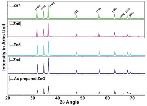
The peaks were more prominent and sharp and matched with the standard card (JCPDS No. 1451).
The highest peak corresponds to the Miller indices (101) plane for Bragg’s angle 36.36°. A slight shift in the diffraction peaks was observed for different annealed samples which can be attributed to the stress in the ZnO structure due to the annealing process. This slight shift at (101) orientation is shown in . For the preferred growth orientation (101), the FWHM (Full-width half maximum-β) was calculated by fitting a Gaussian curve in the origin software and was tabulated in . It is noted that the intensity of the peaks has improved for all annealed samples when compared to the as-prepared ZnO. Zn4 film has the highest intensity as seen from . The values of FWHM decreased with increase in annealing, which is due to heat treatment and grain growth and thus has improvement in the crystallization of the film [Citation35].
Figure 2. Diffraction Spectra of (101) orientation of ZnO and annealed ZnO Thin film
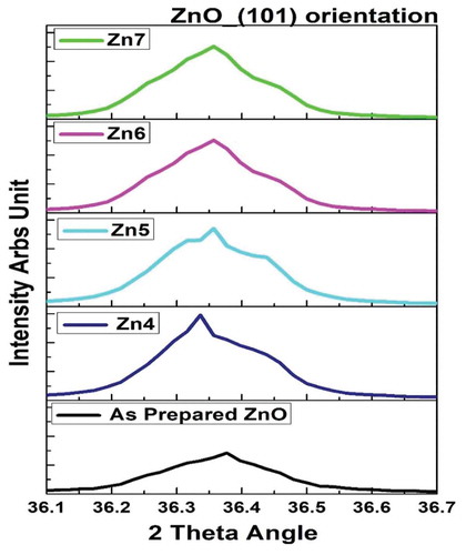
Table 1. Lattice parameters using XRD
sThe lattice parameters “a”, “b” and “c” of hexagonal phase, bond length (L), the volume of the unit cell (V), and grain size (D) were calculated for all the samples at 2θ corresponding to (h k l) plane of (101) and tabulated in using the following Equations (1), (2) and (Equation3(1)
(1) ).
Where λ is the wavelength of incident X-ray (= 1.5405 Å) and θ is Bragg’s angle. The bond length (L) can be calculated using the below equation;
Where
The volume of the unit cell (V) can be calculated by using the below equation;
It is observed that the lattice parameters “a”, “b” and “c” increased due to thermal annealing. But the values are flattened at a higher temperature above 600°C. Also, the volume of a unit cell “V” is high for annealed ZnO samples compared to the as-prepared ZnO film sample.
The grain size (crystallite size) (D) is obtained using Scherrer’s EquationEquation (4)(4)
(4) for all the samples [Citation36,Citation37] are given in .
Table 2. Microstructure analysis using XRD
Where λ is the wavelength of X-rays, β is the FWHM (Full Width at Half Maximum), and θ is the diffraction angle at maximum intensity, i.e. (101) orientation and k is a Scherrer’s constant = 0.94.
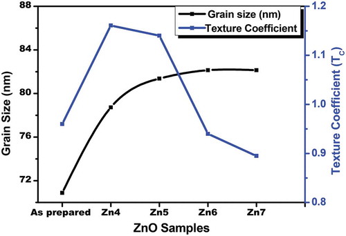
With an increase in annealing temperature, the crystallinity of the film has been increased and thereby, the extent of stoichiometric defects in the form of oxygen vacancies were enhanced. Variation of grain size with annealing temperature is shown in .
Figure 3. Effect of annealing temperature on grain size and texture coefficient of ZnO thin film samples
The effect of annealing temperature on other microstructural parameters such as Tensile strain (ε), Dislocation density (δ) and Texture coefficient (TC) was studied using EquationEquations (5)(3)
(3) , (Equation6
(6)
(6) ) and (Equation7
(7)
(7) ) respectively. The results were tabulated for (101) plane in ,
From , it is observed that with thermal treatment, tensile strain and dislocation density decreased. The decrease in the dislocation density is due to an increase in crystallinity of the film, which transforms into an ordered phase [Citation38].
The texture coefficient (TC) represents the texture of a particular plane, whose deviation from unity implies the preferred growth. Quantitative information concerning the preferential crystallite orientation was obtained from the texture coefficient TC (hkl) using EquationEquation (7)(7)
(7) and is tabulated in [Citation39].
Where I (hkl) is the intensity of the XRD peak corresponding to (101) plane having preferred growth and I0 (hkl) represents the standard intensity (from JCPDS data). N is the number of prominent diffraction peaks (N = 3). The variation of Texture coefficient with annealing temperature for ZnO samples is shown in . It is noted that the Texture coefficient initially increases with increase in annealing temperature and then decreases. This variation is due to stress caused in the film due to the annealing process.
3.2. Optical properties by UV-visible spectrophotometer
The band gap is one of the most important properties of semiconductors and it is studied from the optical absorption measurements with the help of UV-Vis spectrophotometer; UV-1700 Pharma Spec, from SHIMADZU. The optical studies for all the samples are shown in ). From ), it is observed that the highest absorbance of ZnO thin films in the UV region is at 372 nm wavelength. The absorption edge shifted slightly toward the longer wavelengths (redshift) due to the size effect of ZnO nanostructure [Citation40], this shift may be attributing to the improvement of the crystallinity of the films with increasing the annealing temperature.
Figure 4. (a) Absorbance spectra (b) Tauc’s plot of ZnO Thin Film Samples
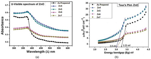
The optical band gap energy (Eg) for all the ZnO samples has been determined using Tauc’s relation, which is described in EquationEquation (8)(8)
(8) and the Tauc’s plot [Citation41] is shown in ).
Where α absorption coefficient, ɦ is Plank’s constant and ϑ is the frequency of incident light, A is constant and Eg is optical band gap of the material.
A graph showing the variation of energy band gap of all ZnO thin film is shown in .
Figure 5. Effect of annealing on energy band gap of ZnO thin film
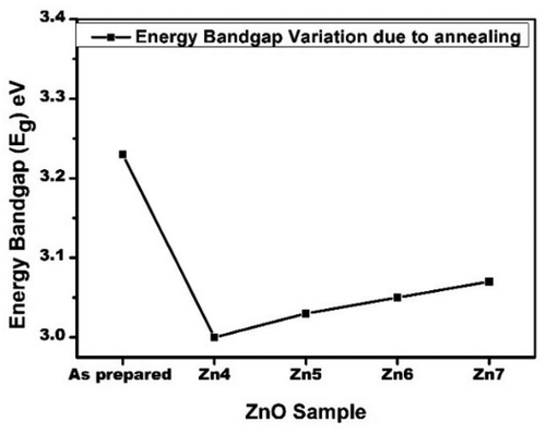
The optical bandgap of ZnO thin film initially decreases from 3.23 eV to 3.0 eV and then increased to 3.07 eV at the higher annealing temperature. The decrease in the optical band gap of the sample can be due to the improved grain size due to annealing [Citation42].
3.3. Structural morphological analysis by FESEM and EDS
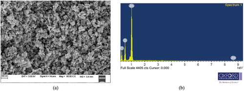
Field Emission Scanning Electron Microscope (FESEM) and Energy Dispersive Spectroscopy (EDS) are carried out for morphology and compositional studies, respectively. Structural morphology of as-prepared ZnO thin film in ) through FESEM using ZEISS showed a uniform hexagonal disc type structure. The EDS of as-prepared ZnO film is shown in ).
Figure 6. (a) FESEM and (b) Energy dispersive spectroscopy images of as-prepared ZnO thin film
Upon annealing, the surface of the film transformed into petal/flower-like structure as the temperature was increased to 400°C–500°C, as seen in ) and (b).
Figure 7. Structural variation of ZnO thin film after annealing for an hour at various temperatures: (a) 400° C (b) 500° C (c) 600° C (d) 700° C
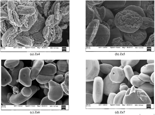
The morphology was becoming more evened out with increased porous and thereby increasing the surface area which can be attributed to thermal decomposition of Zn(OH) 2 at elevated temperature and the formation of a large number of [Zn(OH)4]2-moieties. Some of these decompose to form smaller amounts of ZnO nuclei [Citation43].
These defects in the nano ZnO surface results in improved oxygen vacancy and therefore improve the chemical adsorption. Thus annealing in the range of 400°C-500°C changes the surface of the film, making it more porous, provides a high surface to volume ratio and high aspect ratio, which is more suitable for the applications like gas sensing [Citation44].
It was observed that when the annealing temperature is increased to 600°C-700°C, the surface has become flatter, as seen in ) and (d). The reduction in the porosity of the film and oxygen vacancy may be due to the thermal expansion, where the kinetic energy of the atom increases due to annealing temperatures. Due to the lattice expansion at higher annealed temperature (700°C), the surface becomes more even [Citation45].
EDS (Energy Dispersive Spectroscopy) is used to determine the atomic ratio of Zn to O and the composition of the thin film samples is shown in , using Oxford Instruments, ZEISS.
Table 3. EDS analysis
From , it is visible that the atomic percentile value of Zn is getting larger in the films that are annealed at temperature 400°C, compared to as-deposited film, however at higher annealing temperature 600°C and 700°C, Zn content reduces making it a poor quality film.
3.4. Gas sensing studies
3.4.1. Gas sensing setup
The gas sensing studies were performed in a closed gas exposure chamber at CeNSE Lab, Indian Institute of Science, Bangalore, as shown in ).
Figure 8. Gas sensing setup (a) Gas chamber (b) Electrode assembly (CeNSE Lab, Indian Institute of Science, Bangalore)
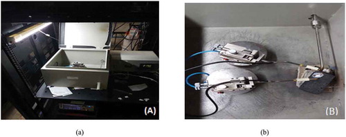
The gas chamber is an assembled system that contains a heater coil connected to a sample holder that decides the operating temperature of the sensor. The system has PC connected with a source meter Keithley 2450. The other end of the source meter is placed on the silver paste, as an electrode of the film which gives the electrical variations of the film in terms of current or resistance when exposed to the target gas.
The NO gas from the cylinder is purged on the film inside the chamber as shown in ), was maintained at a low concentration level of 2.75 ppm, by adjusting the mass flow controller at 500 sccm (standard cubic centimeter per minute).
3.5. Nitric oxide sensing mechanism for different annealed ZnO thin film sensor
ZnO, an n-type of semiconductor material and Nitric oxide is oxidizing type of gas. The gas sensing mechanism involves the change in the surface resistance of the film due to the chemisorption of oxygen onto the surface upon interaction with the gas. During the sensing process, when ZnO thin film is exposed to the air, oxygen molecules are absorbed on the sensor surface as negatively charged ions by capturing the free electrons from the n-type of ZnO which causes an increase in the resistance of n-type ZnO material [Citation46]. In this situation, the sensor is said to be in an equilibrium state, and the resistance becomes a reference resistance.
When the target gas nitric oxide an oxidizing gas is exposed to ZnO film, it is adsorbed on the film. During adsorption, it captures one more electron from the conduction band of the material of the sensor that leads to the chemisorption of nitric oxide to NO− ion. The electron charge carrier in the film reduces, and resistance of the film increases, as seen in . The oxidation-reduction reaction of nitric oxide gas on the surface of the ZnO film is shown in EquationEquation (9)(9)
(9) and (Equation10
(10)
(10) ) respectively.
Figure 9. Nitric oxide gas response – ZnO thin film sensors at an operating temperature of 150°C
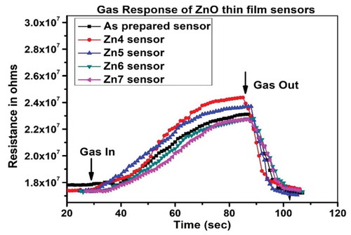
When the nitric oxide gas is taken out of the chamber by allowing the ambient air to plunge into the chamber, the captured electron is released back to the conduction band thereby carrier concentration increases, and the resistance decreases and the sensor reaches back to the equilibrium state as shown in . This change in the resistance is the response or sensitivity of the sensor.
The sensitivity (S) [Citation46] of the sensor is defined as the ratio of the resistance of the sensor in the presence of target gas (NO) to the resistance in the air.
When Rgas > Rair Compared to as-prepared ZnO sensor, annealed ZnO thin film sensors showed a better response. The better response may be due to annealing temperature which enhances the surface to volume ratio and creates active sites on the surface of the film for better adsorption of nitric oxide gas molecules.
From ), it is observed that the ZnO thin film annealed at 400°C (Zn4 sensor) has shown the highest sensitivity (Rg/Ra) of 1.41 as compared to as-prepared ZnO sensor or other annealed ZnO sensors. Graph of sensitivity for all ZnO sensors is shown in ).
Figure 10. At an operating temperature of 150°C (a) Sensitivity (b) Response and recovery time of various ZnO sensors
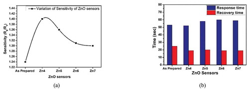
A smart sensor should also be quick in its response. Thus response and recovery time are calculated for all sensors and shown in ). Response time is defined as the time taken by the sensor to reach 90% of the saturation value and the recovery time is defined as the time needed for the sensor to reach back 90% of its equilibrium state [Citation46]. At an operating temperature of 150°C, compared to all annealed sensors, sensor film (Zn4) annealed at 400°C, shows a quick response and recovery time of 52 seconds and 19 seconds, respectively. As evidence from the results of FESEM, that sample annealed at 400°C has provided highly porous structure which is highly suitable as gas sensor.
3.6. The response of Zn4 sensor at various operating temperature toward NO gas
The effect of operating temperature (working temperature) on the sensing response of Zn4 sensor was studied. When the temperature was increased from 150° C to 350° C, the response of the sensor varied and is depicted in ). From the graph, the sensitivity of Zn4 sensor increased with an increase in operating temperature and showed a maximum response of 3.5 at an operating temperature of 300°C and then decreased.
Figure 11. (a) Sensitivity curve (b) Response time and recover time – Zn4 sensor at different operating temperatures
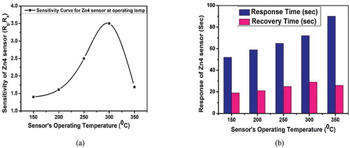
The increase in the sensitivity with higher operating temperature can be attributed to the property of a resistive sensor, where an increase in carrier concentration in the conduction band occurs due to the heating process. The thermal process activates the energy possessed by these electrons which are trapped and released when the gas is in and out, respectively. With different activation energies, a sensor can have different sensitivity. In a real-time application, the sensor essentially needs to have a quick response and recovery time, as the sensitivity can be enhanced by connecting a suitable hardware (embedded System) to the output of the sensor.
The response and recovery time depends on the acceleration of the chemical reaction on the surface of the sensor. The response and recovery time for Zn4 sensor at operating temperature 150°C to 350°C were studied as shown in ). Literature reporting, the response and recovery times of different sensors toward nitric oxide gas are tabulated in . From , it is clear that Zn4 sensor (present work) shows a good sensitivity with quick response and recovery time at a lower operating temperature of 150°C toward 2.75ppm of nitric oxide gas.
Table 4. Response and recovery time for ZnO and other material-based sensors toward NO gas
4. Conclusion
Hexagonal disc structured ZnO thin film is synthesized using spin coating technique and it is annealed at different temperatures such as 400°C, 500°C, 600°C and 700°C. The morphology of the as-prepared and annealed samples showed an increase in grain size and decrease in dislocation density with an increase in annealing temperature. The ZnO thin film transformed in a two-dimensional flower-like structure with highly porous texture on annealing at 400°C and resulted into the high surface to volume ratio suitable for enhanced gas sensing. Optical studies showed the maximum absorbance at a wavelength of 372 nm with reduced bandgap energy with annealing temperature. The Zn4 sample has shown a good response toward 2.75 ppm of nitric oxide at an operating temperature of 150°C with a quick response and recovery times of 52 s and 19 s respectively. We strongly believe that this sensor element can even trace effectively below permissible exposure limit of nitric oxide.
Acknowledgments
Authors are highly grateful for the gas sensing facility provided by CeNSE lab, IISc, Bangalore. One of the Author Dr. P Nagaraju would like to thank DST SERB for providing financial assistance to carry out the present work file number ECR/2016/000534.
Disclosure statement
No potential conflict of interest was reported by the authors.
References
- Fine GF, Cavanagh LM, Afonja A, et al. Metal oxide semi-conductor gas sensors in environmental monitoring. Sensors. 2010;10(6):5469–5502.
- Marchisio A, Tulliani J-M. Semiconducting metal oxides nanocomposites for enhanced detection of explosive vapors. Ceramics. 2018;1(1):98–119.
- Nasiri N, Clarke C. Nanostructured chemiresistive gas sensor for medical applications. Sensors. 2019;19(3):30678070.
- J Gomes, J.J.P.C Rodrigues, R. A. L. Rabelo, N. Kumar and S. Kozlov. IoT-Enabled Gas Sensors: Technologies, Applications, and Opportunities. J of Sensor & Actuator Networks. 2019;8(57). DOI:10.3390/jsan8040057
- Samaneh Matindoust M, Baghaei-Nejad MH, Abadi S, et al. Food quality and safety monitoring using gas sensor array in intelligent packaging. Sens Rev. 2016;36(2):169–183.
- Peng G, Hakim M, Broza YY, et al. Detection of lung, breast, colorectal, and prostate cancers from exhaled breath using a single array of Nanosensor. Br J Cancer. 2010;103(4):542–551.
- Lou Z, Wang L, Jiang K, et al. Programmable three-dimensional advanced materials based on nanostructures as building blocks for flexible sensors. Nanotoday. 2019;26:176–198.
- Comini E, Faglia G, Sberveglieri G, et al. Stable and highly sensitive gas sensors based on semiconducting oxide nano belts. Appl Phys Lett. 2002;81(10):1869.
- Leonardi SG. Two-dimensional zinc oxide nanostructures for gas sensor applications. Chemosensor. 2017;5(2):17.
- Djurisic AB, Chen X, Leung YH, et al. ZnO nanostructures: growth, properties and applications. J Mater Chem. 2012;14(22):6526–6535.
- Yin Zhang TR, Nayak HH, Cai W. Biomedical applications of zinc oxide nanomaterials. Curr Mol Med. 2014;13(10):1633–1645.
- Nath S, Kar JP, Choi J-H, et al. Fabrication and characterization of ZnO single nanowire -based hydrogen sensor. J Phys Chem C. 2010;114(3):1689–1693.
- Omprakash SS, Naveen KSK. Solution-processed amorphous zinc oxide thin film transistor based NAND gate. J Phys. 2020;1455:012023.
- Peksu E, Karaagac H. Synthesis of ZnO nanowires and their photovoltaic application: znO nanowires/AgGaSe2 thin film core-shell solar cell. J Nanomater. 2015;2015:1–10.
- Yoo R, Park Y, Jung H, et al. Acetone-sensing properties of doped ZnO nanoparticles for breath analysis applications. J Alloys Compd. 2019;803:135–144.
- Kim SY, Jeong SH, Lee EY. Skin absorption potential of ZnO nanoparticles. Toxicol Environ Health Sci. 2011;3(4):258–261.
- Jiang J, Pi J, Cai J. The advancing of zinc oxide nanoparticles for biomedical applications. J Bioinorg Chem Appl. 2018;1062562. DOI:10.1155/2018/1062562
- Bhati VS, Hojamberdiev M, Kumar M. Enhanced sensing performance of ZnO nanostructures-based gas sensors: A review. Energy Rep. 2020;6(4):46–62.
- Duoc VT, Le DTT, Hoa ND, et al. New design of ZnO nanorod and nanowire based no2 room–temperature sensors prepared by hydrothermal method. J Nanomater. 2019;6821937. DOI:10.1155/2019/6821937
- Liu F, Wang X, Chen X, et al. Porous ZnO ultrathin nanosheets with high specific areas and abundant oxygen vacancies for acetyl acetone gas sensing. Appl Mater Interfaces. 2019;11(27):24757–24763.
- Wahyuono RA, Schmidt C, Dellith A, et al. ZnO nanoflowers-based photoanodes: aqueous chemical synthesis, microstructure and optical properties. Open Chem. 2016;14(1):158–169.
- Nagaraju P, Vijaykumar Y, Ramana Reddy MV. Room-temperature BTEX sensing characteristics of nanostructured ZnO thin films. J Asian Ceram Soc. 2019;2(2):141–146.
- Yi R, Zhou H, Zhang N, et al. Effects of specific salts on the morphologies of ZnO microstructures. J Alloys Compd. 2009;479(1–2):L50–L53.
- Amin G, Asif MH, Zainelabdin A, et al. Influence of pH, precursor concentration, growth time, and temperature on the morphology of ZnO nanostructures grown by the hydrothermal method. J Nanomater. 2011;269692. DOI:10.1155/2011/269692
- Ozturk S, Kilinc N, Ozturk ZZ. The effect of annealing on gas sensing properties of ZnO nano rod sensors coated with Pd and Pt. Procedia Eng. 2012;47:434–437.
- Khatibani AB. Investigation of gas sensing property of zinc oxide thin films deposited by Sol-Gel method: effects of molarity and annealing temperature. Indian J Phys. 2019. DOI:10.1007/s12648-020-01689-4
- Bhat P, Naveen Kumar SK, Nagaraju P. Synthesis and characterization of ZnO-MWCNT nanocomposites for 1-butanol sensing application at room temperature. Phys B Condens Matter. 2019;570:139–147.
- Nagaraju P, Vijay Kumar Y, Ramana Reddy MV, et al. Effect of vanadium pentoxide concentration in ZnO/V2O5 nanostructured composite thin films for toluene detection. RSC Adv. 2019;9(29):16515–16524.
- Biplob M, Lachit D, Chirosree R, et al. Effect of annealing temperature on the morphology and sensitivity of the zinc oxide nanorods-based methane senor. Acta Metallurgica Sinica (English Letters). 2014;27(4):593–600.
- Zhang JJ, Guo E-J, Wang L-P, et al. Effect of annealing treatment on morphologies and gas sensing properties of ZnO nanorods. Trans Nonferrous Met Soc China. 2014;24:736–742.
- Patil GE, Kajale DD, Shinde SD, et al. Effect of annealing temperature on gas sensing performance of sno2 thin films prepare by spray pyrolysis. Sens Transducers. 2010;9:96–108.
- Quy D. Clinical utility of the exhaled nitric oxide (NO) measurement with portable devices in the management of allergic airway inflammation and asthma. J Asthma Allergy. 2019;12:331–341.
- Prado CM, Martins MA, Tiberio IFLC. Nitric oxide in asthma physiopathology. ISRN Allergy. 2011;2011:1–13.
- Bhat P, Pradhan UU, Kumar SKN. Synthesis and characterization of ZnO nano discs using wet chemical method for sensing applications. Mater Today. 2018;5(4):10763–10770.
- Ghosh PK, Das S, Chattopadhyay KK. Temperature dependent structural and optical properties of nanocrystalline CdO thin films deposited by sol-gel process. J Nanopart Res. 2005;7(2–3):219–225.
- Vijayakumar Y, Nagaraju P, Yaragani V, et al. Nanostructured Al and Fe co-doped ZnO thin films for enhanced ammonia detection. Physica B. 2020;581:411976.
- Shiwen D, Yongtang L. Effect of annealing on microstructure and mechanical properties of magnetron sputtered Cu thin films. Adv Mater Sci Eng. 2015;8. DOI:10.1155/2015/969580
- Aleksandrov LN, Mitlina LA, Kostilov VN, et al. Stresses and dislocation formation in thin films. Phys Status Solidi A. 1994;145(2):255–262.
- Filippo G, Shiwen D, Yongtang L. Effect of annealing on microstructure and mechanical properties of magnetron sputtered Cu thin films. Adv Mater Sci Eng. 2015;1687–8434. DOI:10.1155/2015/969580
- Ungula J, Dejene BF, Swart HC. Effect of annealing on the structural, morphological and optical properties of Ga-doped ZnO nanoparticles by reflux precipitation method. Results Phys. 2017;7:2022–2027.
- Mahmood A, Ahmed N, Raza Q, et al. Effect of Thermal annealing on the structural and optical properties of ZnO thin films deposited by the reactive e-beam evaporation technique. IOP Phys Scr. 2010;82(6):065801.
- Hannas M, Rosli AB, Rusop M. effect of annealing temperature on electrical and optical properties of ZnO thin film prepared by sol gel method. RSM. 2013;227–230. DOI:10.1109/RSM.2013.6706515
- Husna J, Mannir Aliyu M, Aminul Islam M, et al. Influence of annealing temperature on the properties of ZnO thin films grown by sputtering. Energy Procedia. 2012;25:55–61.
- Zhang T, Liu L, Qi Q, et al. Development of microstructure In/Pd-doped SnO2 sensor for low-level CO detection. Sens Actuators B. 2009;139(2):287–291.
- Zhang L, Zhao J, Zheng J, et al. Hydrothermal synthesis of hierarchical nanoparticle-decorated ZnO micro-disks and the structure-enhanced acetylene sensing properties at high temperatures. Sens Actuators B. 2011;158(1):144–150.
- Nagaraju P, Vijayakumar Y, Reddy GLN, et al. ZnO wrinkled nanostructures: enhanced BTX sensing. J Mater Sci Mater Electron. 2018;29:11457–11465.
- Mehta SS, Tamboli M, Mulla I, et al. CTAB assisted synthesis of tungsten oxide nanoplates as an efficient low temperature NOX sensor. J Solid State Chem. 2018;258:256–263.
- Wang S-H, Shen C-E, Jian-Ming S, et al. A room temperature nitric oxide gas sensor based on a copper-ion-doped polyaniline/tungsten oxide nanocomposite. Sensor. 2015;15(4):7084–7095.
- Singh P, Hu L, H W Z, et al. Highly sensitive nitric oxide gas sensor based on ZnO-nanorods vertical resistor operated at room temperature. Nanotechnology. 2018;119396. DOI:10.1088/1361-6528/aaf7cb
- Hong L-Y, Lin H-N. NO gas sensing at room temperature using single titanium dioxide nano dot sensors created by atomic force microscopy nanolithography. Beilstein J Nanotechnol. 2016;7:1044–1051.
- Ramu S, Chandrakalavathi T, Murali G, et al. UV enhanced NO gas sensing properties of the MoS2 monolayer gas sensor. Mater Res Express. 2019;6(8):085075.
- Wei-Chen C, Chin YW, Chun-Han W, et al. Flower-like ZnO nanostructure for NO sensing at room temperature. J Nanosci Nanotechnol. 2016;16(9):9209–9214.
- Tsai Y-T, Chang S-J, Ji L-W, et al. High sensitivity of NO gas sensors based on novel Ag-doped ZnO nano flowers enhanced WITH a UV light-emitting diode. ACS Omega. 2018;3(10):13798–13807.