
 ?Mathematical formulae have been encoded as MathML and are displayed in this HTML version using MathJax in order to improve their display. Uncheck the box to turn MathJax off. This feature requires Javascript. Click on a formula to zoom.
ABSTRACT
The effects of zinc substitution on the electrical properties of sol-gel derived MgNb2O6 (Mg1-xZnxNb2O6; MZxNO) thin films were investigated. Accordingly, the experimental results revealed that the optimal optical and electrical properties of the devices can be obtained for specimen with x = 0.2. The dielectric constant, average transparency and optical band gap of the devices at 400°C annealing are 21.2 (@1 MHz), ~80% and 4.86 eV, respectively. The results indicated that the electrical properties of the sol-gel derived MgNb2O6 thin films are tuneable based upon the variation of zinc content. More importantly, the fabrication temperature of the MZ0.2NO thin films is 100°C lower than the bending point of the glass substrate making it suitable for practical applications. With the increase of the applied electric field, the leakage conduction mechanisms of the Al/MZxNO/ITO devices are mainly controlled first by ohmic conduction at low electric field, changes to space-charge-limited conduction (SCLC) and then FN tunneling at high electric field. Moreover, the critical electric field strength of the conduction mechanisms is also a function of the zinc content.
1. Introduction
Transparent oxide film is an indispensable part of the development of transparent electronics and has been applied for several applications [Citation1,Citation2]. However, the un-avoidable high-temperature crystallization process may lead to a rough surface and higher leakage current in the films. An alternation of the crystalline films by using an amorphous material is one of the choices for novel transparent electronic applications that may offer several advantages, including lower processing temperatures and leakage current, better surface uniformity, and superior mechanical flexibility [Citation3,Citation4]. Among these dielectric materials, MgNb2O6(MNO) is known as a popular microwave dielectric [Citation5], optoelectronic and photoactive material due to the excellent dielectric properties, good thermal stability and wide optical band gap. These superior properties also make MNO a potential candidate to replace the dielectric layer in the transparent electronics or multifunctional optoelectronics.
In our previous work [Citation6], highly transparent amorphous-MNO thin films on indium tin oxide (ITO)/glass substrates were fabricated by the sol-gel method, and the effects of annealing temperature and atmospheres (N2, air and O2) on the electrical and optical properties of these films were also discussed [Citation6,Citation7]. The results indicated that the amorphous MNO thin films featured a high dielectric constant, low leakage current and good transparency after 500°C annealing. In addition, the electrical properties of amorphous MNO thin films can be easily tuned via the O2/N2 ratio during annealing, which is related to the ratio of Nb4+/Nb5+ content in the films. The percentage of Nb4+ content increased when the films were annealed in the oxygen-deficient conditions, which could lead to semiconducting films; in contrast, annealing in an oxygen-rich environment could lead to dielectric films. Moreover, the conduction mechanisms of MNO/ITO heterojunctions were also transferred by annealing. The experimental results suggest that amorphous MNO films have considerable potential for use in multifunctional optoelectronics, due to their smooth surfaces, flexible electrical properties and good transparency.
In comparison with crystalline MNO [Citation8–10], the amorphous MNO is more promising for low-temperature applications. However, it required a 500°C annealing which is close to the bending point of the glass. Metallic oxides are commonly used as a dopant to reduce the fabrication temperature of the devices [Citation11]. Since the radius of Zn2+ and Mg2+ are similar, ZnO was selected as a dopant to lower the fabrication temperature of the sample. Moreover, the effect of the Zn substitution on the electrical and optical properties of the amorphous MNO thin films was also investigated in this study.
2. Materials and methods
Magnesium acetylacetonate dihydrate (C10H14MgO4.2H2O, >98%, Alfa Aesar), Zinc acetate dihydrate [Zn(CH3COO)2.2H2O, >99%, Alfa Aesar] and Niobium ethoxide [Nb(OC2H5)5, 99.999%, SIGMA-ALDRICH] were dissolved in 1-Butanol (C4H10O, >99.4%, J. T. Backer) to form the precursor solution (0.1 M). The molar ratio of the (Mg+Zn) and Nb precursors was fixed at 1:2, with acetylacetone (C5H8O2, 99%, Alfa Aesar) used as the stabilizing reagent. Then, the precursor sol was spin-coated on the glass and ITO/glass substrates. The detail of the deposition procedure is shown in our previous work [Citation6,Citation7]. Finally, the Mg1-xZnxNb2O6(MZxNO) films were annealed at 400°C and 500°C for 30 min in air. The heating rate was fixed at 2°C/min, and the final thickness of the films was about 60 nm after annealing.
The crystalline structure was analyzed by grazing-incidence X-ray diffraction (GIXRD, Rigaku D/Max III, V) using Cu Kα radiation at 40 kV and 100 mA; the surface morphology was observed using field emission scanning electron microscopy (FESEM, HITACHI SU-8000) in SEI mode. In order to identify the chemical states and composition of the thin films, X-ray photoelectron spectroscopy (XPS, ULVAC-PHI PHI5000; C1s as a reference at 284.8 eV) with Al Kα monochromatized source was used in this study. In order to estimate the brief energy band diagram of the device, the absorbance spectra were directly obtained by a UV-visible spectrophotometer and the valence band maximum of the samples were measured by UV photoelectron spectra (UPS) which was carried out with the He I line (21.2 eV). To minimize the influence of surface contamination, all samples were degassed in an entry chamber for 30 min and transferred to the main chamber sputtered with low dosage Ar+ ions to remove the surface contamination. The main chamber pressure was then maintained in the range 10−8 Pa.
The optical transmittance spectra of the MZxNO/quartz structure were measured using a UV-visible recording spectrophotometer (UV-vis, HITACHI U4100) from 200 to 800 nm. To form the Al/MZxNO/ITO/glass MIM structure, 200 nm Al electrodes with a diameter of 1 mm were deposited by E-beam evaporation. The capacitance-voltage (C-V) and current-voltage (I–V) measurements of the MIM capacitor were obtained using an Agilent E4980A LCR meter and Agilent E5270B Parameter Analyzer.
3. Results and discussion
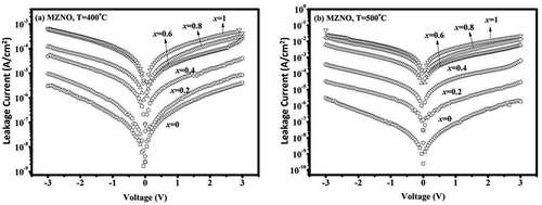
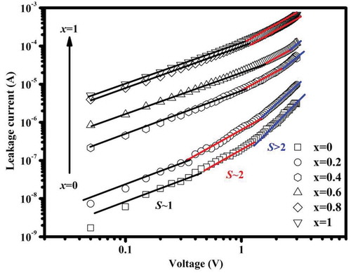
shows the GIXRD patterns of the MZxNO samples annealed at 400°C and 500°C. All samples revealed amorphous-like patterns after 400°C annealing. As the annealing temperature increased to 500°C, clear diffraction peaks identified as columbite-M2+Nb2O6 (M = Mg or Zn) phase were observed. Based on the findings of our previous study [Citation6,Citation7], the crystalline temperature of the MNO films is over 600°C. These results indicated that the crystalline temperature of the magnesium-based columbite thin films could be effectively reduced by zinc substitution. The average grain size was estimated by using the cross line method and listed in . A slight grain growth could be observed in the 500°C-annealed films with the x content increasing due to the improvement in the crystallinity. ) and (b) illustrate the plane view of FESEM figures of the MZxNO samples annealed at 400°C and 500°C, respectively. According to the FESEM results, MZxNO films exhibited a smooth and uniform surface morphology when the annealing temperature was lower than 500°C. The current-voltage (I–V) characteristics of the Al/MZxNO/ITO/glass MIM capacitors are shown in . With the increase of Zn content, the leakage current increased from 3 × 10⁻⁷ to 1 × 10⁻⁴A and from 8 × 10⁻⁸ to 4 × 10⁻³ A at 1 V for samples annealed at 400°C and 500°C, respectively. Moreover, the leakage current also increased with the increase of annealing temperature due to a higher film density as shown in . The 500°C-annealed film revealed a higher density leading to a higher leakage current. The I–V curves revealed almost symmetric behavior within −3 V~+3 V range may be owing to that the work function of Al and ITO are similar. In order to obtain a high quality amorphous transparent dielectric film for transparent optoelectronics, the chemical, optical and electric properties of 400°C-annealed samples are discussed below.
Table 1. The grain sizes of the 500°C-annealed MZxNO films
Figure 1. GIXRD patterns of MZxNO thin films
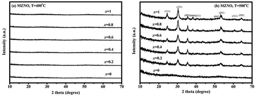
Figure 2. FESEM of the MZxNO samples annealed at (a) 400°C and (b) 500°C
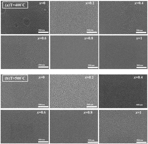
Figure 3. J-E relations of the Al/MZxNO/ITO/glass MIM capacitors annealed at (a) 400 and (b) 500°C
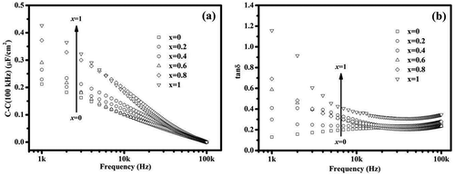
XPS was used to confirm the chemical bonding states of the films. The characteristic spectra of the 400°C-annealed films (x = 0, 0.2, 0.6, 1) are shown in . The binding energy for Mg 2p and Zn 2p revealed divalent oxidation states, which are very similar to those found in our previous work [Citation6,Citation7]. The O 1s and Nb 3d spectra of the films could be decomposed clear shoulders (non-lattice oxygen and Nb4+). The binding energy for the lattice oxygen signal is at 529.6 eV, which indicates the metallic-oxygen bonding while the non-lattice oxygen signal is at 531.02 eV [Citation12]. The Nb 3d spectra showed two main peaks for Nb 3d3/2 and Nb 3d5/2, which can both be assigned to a pentavalent oxidation state. The energy difference between Nb 3d5/2 and Nb 3d3/2 is 2.72 eV in all cases. According to the literatures [Citation13,Citation14], the presence of Nb4+ within MgNb2O6 films may act as an n-type dopant which may highly affect the electric properties of the films. The area ratio of the decomposed peaks of lattice oxygen (Olattice), non-lattice oxygen (Onon-lattice), Nb5+ and Nb4+ are shown in . However, no obvious change in the Nb4+ratio of the MZxNO films at various x contents. Therefore, the effect of Nb4+ratio of films can be excluded from the dominant factor of the variation of the electrical properties. The transmittance spectra () of the 400°C-annealed MZxNO/quartz samples indicated that the transmittance of the samples was near 80% in the visible range. It is worth mentioning that a cleared-shift in the optical absorption band edge appeared when the x value increased. In order to clarify the effect of zinc substitution on the optical property of MZxNO samples, the optical band gap of MZxNO films was investigated and ranging from 4.69 to 4.95 eV as the x value varied from 1 to 0. The plots of capacitance-voltage (C-V) and loss-voltage (tanδ-V) of the Al/MZxNO/ITO/glass MIM capacitors are illustrated in ) and (b), respectively. In C-V measurement, oscillator level is fixed at 0.05 V. The measured capacitances (and tanδ) of the samples are ranging from 1.62 nF (0.14) for MgNb2O6 to 3.24 nF (0.62) for ZnNb2O6 at 100 kHz for the 400°C-annealed samples. In order to get more insight into the effect of space charge in these samples, C-f and tanδ-f curves measured from 1 kHz to 100 kHz are presented. In ) and (b), C − C (100 kHz)-f and tanδ-f values are given to allow a direct comparison, where C (100 kHz) is the capacitance measured at 100 kHz. A large difference in capacitance and dielectric loss can be found between 1 and 10 kHz, especially when the zinc content becomes significant. In XPS results, no obvious variation in the Nb4+/Nb5+ ratio could be found in these samples. One possible reason for the high dielectric constant and leakage current in the samples with high Zn content may be due to the high ionic polarization of Zn or Zn interstitial [Citation13]. However, the film density increased (porosity decreased) with the increase of Zn content as can be seen in ). Therefore, the high dielectric constant and leakage current of the samples was more likely attributed to the density of the films.
Table 2. The area ratio of the XPS peaks of the 400°C-annealed MZxNO films
Figure 4. XPS core spectra of the (a) Mg 2p, (b) Zn 2p, (c) O 1s and (d) Nb 3d signals of the400°C-annealedMZxNO films
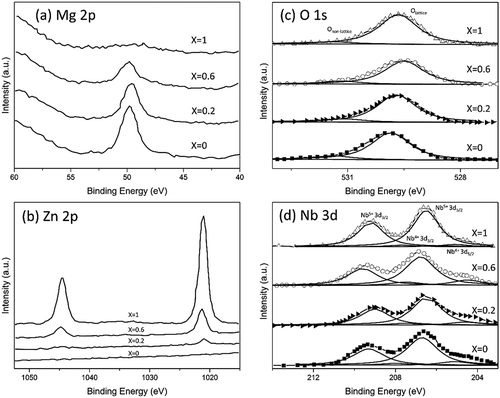
Figure 5. (a) Transmittance spectra and (b) bandgap plot of the MZxNO/quartz
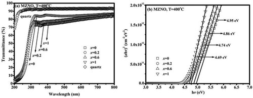
Figure 6. (a) C-V and(b) tanδ-V relations of the Al/MZxNO/ITO/glass MIM capacitors annealed at 400°C
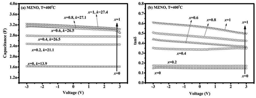
Figure 7. (a)C-f and(b) tanδ-f relations of the Al/MZxNO/ITO/glass MIM capacitors annealed at 400°C
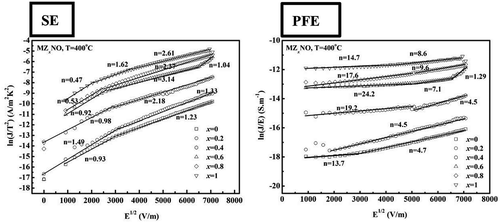
According to the past research [Citation6], the fluctuation in the leakage current of the samples produced under various conditions may be due to the variation of the conduction mechanisms, which is related to the Nb4+ (or oxygen vacancy) concentration. The re-plotted I–V curves shown in revealed that the calculated K values deviate from the expected ones (K ~ 4) [Citation6]. Therefore, SE and PFE should be excluded from discussions of the conduction mechanism of the MZxNO samples in this work. Interface-limited Fowler-Nordheim (FN) tunneling and space-charge-limited conduction (SCLC) are also considered.
Figure 8. SE and PFE plots of the Al/MZxNO/ITO/glass MIM capacitors annealed at 400°C
shows the double logarithmic I–V curves for the MZxNO samples. The typical I–V characteristics for the SCLC in the double-log I–V plot can be divided into three regions. When the applied voltage is low, the slope of the double-log I–V curve is near 1, which implies that the current depends on the applied voltage and this behavior is like the Ohmic conduction mechanism (). Next, the slope of the double-log I–V curve is about 2. It is assumed that the injected electrons are partly trapped by the thin film, while the others not trapped contribute to the current. This behavior is similar to traps-filled limitation (
). Not until all existing trapping centers in the thin film are occupied, the subsequently injected electrons are free to move in the thin film. Finally, if the current is fully controlled by the space charges, which were built up by the injection electrons and limit the further injection electrons, the current is proportional to the voltage square [Citation15].
Figure 9. The double logarithmic I–V relations of the Al/MZxNO/ITO/glass MIM capacitors annealed at 400°C
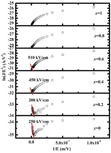
The relation for the MZxNO samples is shown in . FN tunneling is the quantum effect by which the electrons do not overcome the barrier, but flow through. A roughly straight line fitting with a negative slope in the high electric region shown in the MZxNO (x = 0–0.6) samples suggested that when a high electric field is applied, the dominant leakage mechanism of the MZxNO samples is FN tunneling.
Figure 10. The ln(J/E2)-1/E relations of the Al/MZxNO/ITO/glass MIM capacitors annealed at 400°C
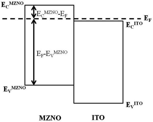
Considering the positive voltage portion of I–V curve, the conduction mechanisms of bottom injection (MZxNO/ITO interface) of the MZxNO samples are summarized in . The results revealed that all of the MZxNO samples followed an ohmic behavior under a low electric field suggesting that the barrier height between ITO and MZxNO is small enough for the electrons to pass through directly. Moreover, the samples showed an SCLC behavior under strong injection conditions (high electric field) as the density of trapped charges in the MZxNO films became significant [Citation16]. These results can be partially confirmed by the above mentioned XPS data: the Nb4+ existed in the MZxNO films, and the injected electrons were then trapped by the oxygen vacancies, leading to the SCLC. When the electric field is high enough, the MZxNO conduction band crosses the position of the ITO Fermi level and then tunneling occurs [Citation14]. To further understand the leakage mechanisms of the MZxNO samples, the valence band spectra () were measured by UPS to obtain the schematic energy band diagram of the MZxNO/ITO stack. The difference of the Fermi level and the valence band maximum (VBM) for the ITO substrate, MgNb2O6, MZ0.2NO, MZ0.6NO and ZnNb2O6 are found to be 2.55, 3.55, 3.73, 3.97 and 4.1 eV, respectively, which can be determined by the linear extrapolation of spectra. The energy band diagram of the MZxNO/ITO heterostructure can be deduced as demonstrated in , where ECMZNO, EVMZNO, and ECITO, EVITO are the conduction band minimal and valence band maximum values of the MZxNO and ITO, respectively. When a positive bias applied on the top electrode is large enough, the MZxNO conduction band crosses the position of the ITO Fermi level and tunneling occurs. The calculated values of the band diagram of the MZxNO samples are shown in . From the data, ECMZNO-EF value of the MZxNO samples increased with the increase of x value. This result also provided a well explanation of the increase of onset tunneling field (EFN) as the x value increased.
Table 3. Summary of the conduction mechanisms of MZxNO samples
Table 4. The calculated values of the band diagram and EFN of the MZxNO samples
Figure 11. The valence band spectra of the 400°C-annealed MZxNO samples
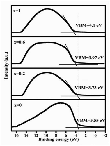
Figure 12. The energy band diagram of the MZNO/ITO heterostructure
4. Conclusion
In summary, the optical band gaps of the MZxNO films decreased from 4.69 to 4.95 eV as the x value varied from 1 to 0. Also, the leakage current densities (J), dielectric constant and tanδ of the samples are increased as the x value increased. The fluctuation in the leakage current of the samples is Zn content related. All of the MZxNO samples followed an ohmic behavior under a low electric field suggesting that the barrier height between the ITO and the MZxNO is small enough for the electrons to directly pass through. On the other hand, the FN tunneling occurs when the samples were subject to a high applied bias. The experimental results also revealed that the onset tunneling field (EFN) is a function of the Zn content.
Acknowledgments
The authors gratefully acknowledge the use of D8 Discover equipment belonging to the Instrument Center of National Cheng Kung University.
Disclosure statement
The authors declare that they have no known competing financial interests or personal relationships that could have appeared to influence the work reported in this paper.
Additional information
Funding
References
- Gao L, Song Z, Li Y, et al. Switching failure behaviors and doping enhanced performances of Ni/Al2O3/p+Si resistive switching devices. J Appl Phys. 2019;125(24):245306. .
- Hongbin Z, Hailing T, Feng W, et al. Highly transparent dysprosium oxide-based RRAM with multilayer graphene electrode for low-power nonvolatile memory application. IEEE Trans Electron Devices. 2014;61(5):1388–1393. .
- Liu J, Buchholz DB, Hennek JW, et al. All-amorphous-oxide transparent, flexible thin-film transistors. Efficacy of bilayer gate dielectrics. J Am Chem Soc. 2010 Sep 1;132(34):11934–11942.
- Medvedeva JE, Buchholz DB, Chang RPH. Recent advances in understanding the structure and properties of amorphous oxide semiconductors. Adv Electron Mater. 2017;3(9):1700082.
- Khalam LA, Thomas S, Sebastian MT. Tailoring the microwave dielectric properties of MgNb2O6 and Mg4Nb2O9 ceramics. Int J Appl Ceram Tech. 2007;4(4):359–366.
- Ho Y-D, Chen K-R, Yu P-C, et al. The effects of annealing atmosphere on the electrical properties of MgNb2O6/ITO heterostructures. J Am Ceram Soc. 2015;98(2):580–586. .
- Ho Y-D, Chen K-R, Huang C-L, et al. Sol-Gel-derived amorphous-MgNb2O6Thin films for transparent microelectronics. J Am Ceram Soc. 2013;96(11):3375–3378. .
- Ananta S, Brydson R, Thomas NW. Synthesis, formation and characterisation of MgNb2O6 powder in a columbite-like phase. J Eur Ceram Soc. 1999;19(3):355–362.
- Sarkar K, Mukherjee S. Synthesis, characterization and property evaluation of single phase MgNb2O6 by chemical route. J Aust Ceram Soc. 2016;52(2):32–40.
- Wu C, Hu Y, Bao S, et al. Microwave dielectric properties of low-temperature-fired MgNb2O6 ceramics for LTCC applications. RSC Adv. 2020;10(50):29835–29842. .
- Banger KK, Peterson RL, Mori K, et al. High performance, low temperature solution-processed barium and strontium doped oxide thin film transistors. Chem Mater. 2014 Jan 28;26(2):1195–1203.
- Goh Y, Cho SH, Park SHK, et al. Oxygen vacancy control as a strategy to achieve highly reliable hafnia ferroelectrics using oxide electrode. Nanoscale. 2020 Apr 28;12(16):9024–9031.
- Hutson AR. Hall effect studies of doped zinc oxide single crystals. Phys Rev. 1957 Oct 15;108(2):222–230.
- Lipp E, Shahar Z, Bittel BC, et al. Trap-assisted conduction in Pt-gated Gd(2)O(3)/Si capacitors. J Appl Phys. 2011 Apr 1;109(7):073724.
- Lim EW, Ismail R. Conduction mechanism of valence change resistive switching memory: A survey. Electronics-Switz. 2015 Sep;4(3):586–613.
- Luo JM, Lin SP, Zheng Y, et al. Nonpolar resistive switching in Mn-doped BiFeO3 thin films by chemical solution deposition. Appl Phys Lett. 2012 Aug 6;101(6):062902.