
 ?Mathematical formulae have been encoded as MathML and are displayed in this HTML version using MathJax in order to improve their display. Uncheck the box to turn MathJax off. This feature requires Javascript. Click on a formula to zoom.
ABSTRACT
In this paper, we proposed a technique, ultrafast laser machining–picosecond laser welding, to fabricate an embedded thin film by placing a coating material (ZnO powders) between the interface of two glass substrates. We researched the thickness (embedding depth of ZnO powders) and the formation mechanism of the embedded thin film and the zinc content and distribution. Under our experimental conditions, an embedded thin film of 600 μm thickness was formed. At a distance of 340 μm within the embedded thin film, the zinc content peaked at 400 cps. Finally, we fabricate an embedded thin film with the bonding strength of 12.22 MPa. This technique breaks through the bottlenecks of thin films fabricated by conventional lasers, such as long duration, low precision and serious chemical pollution, which has great significance for achieving high-end manufacturing of thin-film devices.
1. Introduction
A thin-film device is a functional device for modern high-tech applications [Citation1–4]. It has extensive application prospects [Citation5,Citation6] in the areas of semiconductor integrated circuits [Citation7–11], optical components [Citation12–15] and biomedical instruments [Citation14–17]. To fabricate thin films, there are three traditional laser processing methods: laser chemical vapor deposition (LCVD) [Citation18–20], pulsed laser deposition (PLD) [Citation21–23] and matrix-assisted pulsed laser evaporation (MAPLE) [Citation24]. Since the 1960s, many scholars have conducted many studies on the above traditional laser processing methods. Although the traditional methods of fabricating thin films have the advantages of extensive application range and high practicality, there are defects such as long duration, low precision and serious chemical pollution; thus, these traditional methods restrict the application scale of thin-film devices.
In this research, we fabricated a type of embedded ZnO thin-film by picosecond laser (one type of ultrafast laser) glass welding, which can be used for manufacturing thin-film devices. In particular, the thickness and the formation mechanism of the embedded thin film and the zinc content and distribution are discussed. This method has the advantages of high efficiency, high precision, environmental friendliness. In addition, double-layer films of two glass substrates can be simultaneously formed by the up and down movement of plasma, and we can make different functional thin-film devices if we change the coating material. Consequently, the application prospects of thin-film devices can be enlarged because of these advantages.
2. Experimental setup and welding process
2.1. Experimental setup
The apparatus in this research includes a picosecond laser system, a 3D translation stage, a pneumatic glass fixture and a computer system, as shown in . The parameters of the picosecond laser system are set as follows: the pulse duration is 10 ps, the wavelength is 1064 nm, and the repetition rate is 1 kHz. The laser beam is focused on the interface of two glass substrates (10 mm × 10 mm × 0.5 mm, JGS2) by an objective lens. The characterizations and corresponding values of JGS2 substrate before welding are shown in . In our experiment, the glass substrates are moving at different speeds, which are controlled by a 3D translation stage connected to the computer system, while the laser source is fixed.
Figure 1. Experimental setup.
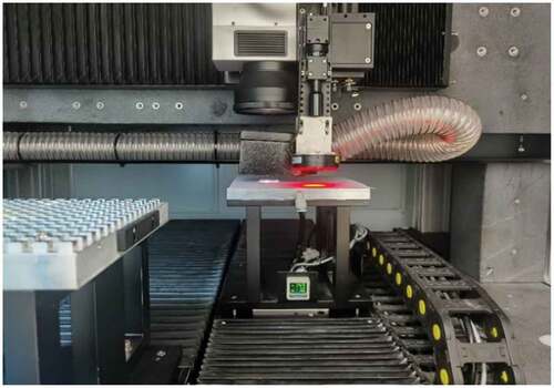
Table 1. The characterizations and corresponding values of JGS2 substrate before welding.
There are many choices for the coating material in our experiment, such as silver powders, copper powders, nickel powders, zinc powders, tungsten powders, zinc oxide powders, aluminum alloy powders, magnetic powders, ceramic powders, and carborundum powders. In this paper, we choose ZnO powders (diameter of 20 nm) as the coating material. To avoid personal errors, we perform the experiment 10 times and calculate the average value.
2.2. Welding process
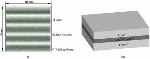
illustrates the fabrication of an embedded thin film between two glass substrates by picosecond laser welding. Before fabrication, we cleaned the glass substrates in an ultrasonic bath and dried them in the air. Then, glass 2 was fixed on the 3D translation stage. The ZnO powder (1 mg) was evenly placed on the glass 2, after which glass 1 placed on top of glass 2. We focused a picosecond pulse laser on the ZnO powder layer. According to the set welding route in , the welding process was achieved by the computer system used to control the picosecond laser system and 3D translation stage.
Figure 2. Schematic of the welding process of an embedded thin film. (a) Two-dimensional diagram. (b) three-dimensional model.
3. Mechanism
When the picosecond laser focused on the interface of the two glass substrates, vaporization, ionization and phase explosion occurred on the interface of the glass substrates because of the ablation of ZnO powders and glass by the picosecond laser. Meanwhile, many ZnO nanoparticles, such as ions, electrons and atoms, sputtered out of the interface. The ZnO nanoparticles expanded under the continuous action of the picosecond laser, and then, they formed ellipsoid plasma plumes with local high temperature and high pressure. An embedded thin film was formed at the interface by the up and down movement of the plasma [Citation25] and its diffusion into the SiO2 network of the glass surface.
The laser power and welding speed are the key factors affecting the shape of the molten pool and the flow velocity of ZnO nanoparticles. The shape of the molten pool is mainly featured in the diameter and depth of the molten pool. The molten pool depth and the flow velocity of the ZnO nanoparticles in the molten pool determine the embedding depth and the embedding capacity of the ZnO powders. Under lower welding speed conditions, the recoil pressure in the molten pool increases due to the surface temperature rise, which pushes ZnO nanoparticles downwards and causes downward convection. The downward convection drives heat from the molten pool surface to the middle zone, which leads to zinc element downward movement and uneven distribution [Citation26].
4. Result and discussion
In this research, the control variables among the experimental parameters were used to explore the welding quality, as shown in . First, the line spacing of the welding route and the welding speed were set as 0.05 mm and 70 mm/s (groups 1 to 3 and groups 11 to 13). Under this condition, the average power was increased from 17.5 W to 25 W, but only when the average power was 20 W could welding be achieved. The possible reasons are as follows: when the average power was less than 20 W, the heat accumulation was too low to form a large molten pool, and welding could not be achieved. When the average power was greater than 20 W, the heat accumulation was so high that the glass easily cracked and might swell up, and a reliable connection could not be realized. Then, the average power and line spacing of the welding route were set as 20 W and 0.05 mm (groups 3 to 7). Based on the fixed average power and line spacing of the welding route, the welding speed was increased from 50 mm/s to 90 mm/s, and welding could be achieved under the condition of 70 mm/s. The reasons were thought to be as follows: when the welding speed was low, the heat accumulation was so high that cracks might easily appear, and reliable welding could not be achieved. When the welding speed was higher than 70 mm/s, the heat accumulation was not sufficient to form a large molten pool, so the samples could not be welded. In addition, we set the average power and welding speed 20 W and 70 mm/s (groups 3, 8, 9, and 10). The line spacing of the welding route was changed from 0.01 mm to 1 mm, and welding could be achieved. This result indicated that the line spacing of the welding route has little effect on the bonding strength, but in this range, the smaller the line spacing of the welding route was, the better the thin film formed. Corresponding to the formation mechanism in section 3 and the above analysis, present images of the embedded thin film fabricated with an average power of 20 W, a welding speed of 70 mm/s, a line spacing of the welding route of 0.01 mm, a pulse duration of 10 ps, a wavelength of 1064 nm and a repetition rate of 1 kHz.
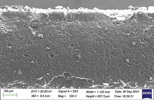
Figure 3. SEM Image of the embedded thin film (one of the glass substrates was randomly selected).
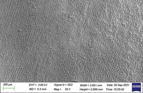
Figure 4. Detailed SEM image of the embedded thin film.
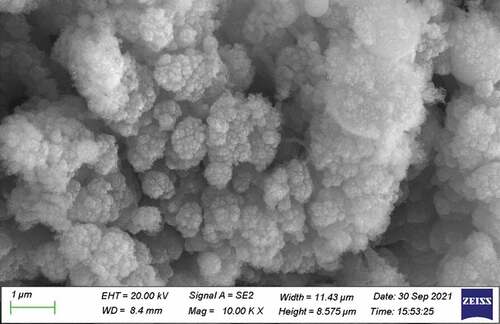
Table 2. Welding effect based on different parameters.
shows the full cross section of the embedded thin film. The embedded depth of the ZnO powders reached 600 μm, which was measured by scanning electron microscopy.
Figure 5. Full cross section of the embedded thin film.
depicts the zinc content and distribution in the embedded thin film detected by EDS. We can see that the zinc content presents a nonuniform distribution corresponding to different embedding capacities of the ZnO powders throughout the full cross section of the embedded thin film.
Figure 6. Zinc content and distribution in the embedded thin film.
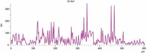
Based on the above mechanism of the laser power and welding speed affecting the embedding depth and embedding capacity of ZnO powders in section 3, quantitative control of the embedding depth and embedding capacity of ZnO powders can be realized by changing the average power and welding speed to manufacture different embedded thin films that suit a wide range of requirements. In addition, the melting point of SiO2 (1723°C) is much lower than that of ZnO (1975°C), and the action of the recoil pressure in the molten pool contributes to the solid ZnO powders flowing down into molten SiO2. Then, the ZnO powders melt with the increasing temperature and mixes with the molten SiO2, being unequally distributed by downward convection. The maximum zinc content (400 cps) occurred in the middle (at a distance of 340 μm) of the embedded thin film.
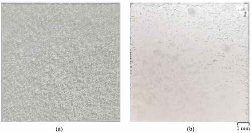
displays the difference in the appearance between two glass substrates before and after welding. presents two glass substrates with evenly distributed ZnO powders before welding; and exhibits two glass substrates with embedded thin film after welding, although there are some defects in the corners and in the middle. Obviously, the embedded thin film is white and opaque, which has many potential applications in absorbing material, especially electromagnetic wave absorbent, and the selective absorbing properties depend on the thickness of thin film, Zn content, Zn distribution, etc.
Figure 7. The comparison of glass substrates before and after welding. (a) Two glass substrates with evenly distributed ZnO powders before welding. (b) Two glass substrates with an embedded thin film after welding.
In comparison with , illustrates the characterizations and corresponding values of JGS2 substrate after welding.
Table 3. The characterizations and corresponding values of JGS2 substrate after welding.
The surface flatness of JGS2 substrate was measured by 9-point measurement method with Fully Automatic Image Measuring Instrument (Jateng QVS3020CNC, resolution of 0.5 µm). Data shows that the overall surface flatness of the substrate is 6 µm before welding. But in contrast, after welding, it becomes 7 µm on more than 99.5% surface-coated region and 8 µm or 9 µm with the remaining region. Within the tolerance range less than 0.5%, it presents a promising technique to fabricate high precision ZnO thin-film glass components for electromagnetic wave absorption.
In order to measure the bonding strength, we set a measuring instrument. The instrument is described as follows: firstly, the front of the glass 1 was connected to a string fixed to a pole and the back of the glass 2 was connected to a container by a string. The measuring instrument was in a vertical state. And then, we added some sand into the container until the glasses were cleaved. Finally, we converted the weight of the container and the sand in the container to the value of bonding strength. In practice, 12.22 MPa was applied to separate the bonded substrates, which can satisfy the demand in an industrial application for glass welding.
5. Conclusion
This paper presents a method based on ultrafast laser welding technology to fabricate embedded thin films by placing ZnO powders between the interface of two glass substrates. An embedded depth of 600 μm ZnO thin-film was fabricated and the maximum zinc content (400 cps) was presented at the distance of 340 μm of the embedded thin film. After welding, the overall surface flatness of the substrate is 7 µm on more than 99.5% areas, which is less than 0.5% tolerance range compared to surface flatness before welding. And the bonding strength of embedded thin-film glass substrates reached 12.22 MPa under the condition of average power 20 W, welding speed 70 mm/s, a line spacing of the welding route 0.01 mm, pulse duration 10 ps, wavelength 1064 nm and a repetition rate 1 kHz. In this case, we obtained the best thin film under our experimental condition. This method offers a new idea for manufacturing thin-film devices and provides important academic value and economic benefits to realize high-tech applications in electromagnetic wave absorption.
Future work can continue this study in the following two aspects. First, the welding process conditions, such as the fixed high repetition rate, continuous line welding, single irradiation and one-layer irradiation, can be replaced by periodically alternating high repetition rates, discontinuous skip welding, multiple irradiations and multilayer irradiation. Second, embedded thin films with different functions can be fabricated by changing the coating material.
Disclosure statement
No potential conflict of interest was reported by the author(s).
Additional information
Funding
References
- Bhardwaj S, Gupta A, Kumar G, et al. Comparative structural and optical studies of Al-/Sn-doped ZnO-textured films for optoelectronic application. J Mater Sci: Mater Electron. 2022;33:13757–13770.
- Kumar S, Sharma P, Sharma V. Structural transition in II-VI nanofilms: effect of molar ratio on structural, morphological, and optical properties. J Appl Phys. 2012;111(11):113510.
- Zaka H, Parditka B, Erdélyi Z, et al. Investigation of dispersion parameters, dielectric properties and opto–electrical parameters Of ZnO thin film grown by ALD. Optik. 2020;203:163933.
- Sharma P, Sharma N, Sharda S, et al. Recent developments on the optical properties of thin films of chalcogenide glasses. Prog Solid State Ch. 2016;44(4):131–141.
- Zheng G, Zhu P, Sun L, et al. Thin film zinc oxide gas sensor fabricated using near-field electrospray. AIP Adv. 2016;6(12):125306.
- Zeijl HWV. (Invited) Thin film technologies for micro/nano systems; a review. ECS Trans. 2014;61(3):191–206.
- Davis RF, Kelner G, Shur M, et al. Thin film deposition and microelectronic and optoelectronic device fabrication and characterization in monocrystalline alpha and beta silicon carbide. Proc IEEE. 1991;79(5):677–701.
- Fortunato E, Barquinha P, Martins R, et al. Oxide semiconductor thin-film transistors: a review of recent advances. Adv Mater. 2012;24(22):2945–2986.
- Han HC, Chong CW, Wang SB, et al. High k nanophase zinc oxide on biomimetic silicon nanotip array as supercapacitors. Nano Lett. 2013;13(4):1422–1428.
- Liu N, Wei F, Liu L, et al. Optically-controlled digital electrodeposition of thin-film metals for fabrication of nano-devices. Opt Mater Express. 2015;5(4):838–848.
- Paula KT, Gaál G, Almeida GFB, et al. Femtosecond laser micromachining of polylactic acid/graphene composites for designing interdigitated microelectrodes for sensor applications. Opt Laser Technol. 2018;101:74–79.
- Song YM, Lee YT. Micro/nano combined structure, manufacturing method of micro/nano combined structure, and manufacturing method of an optical device having a micro/nano combined structure integrated therewith. United States patent US 0,128,362. 2013 May 23.
- Aslan MM, Webster NA, Byard CL, et al. Low-loss optical waveguides for the near ultra-violet and visible spectral regions with Al2O3 thin films from atomic layer deposition. Thin Solid Films. 2010;518(17):4935–4940.
- Brüggemann D. Nanoporous aluminium oxide membranes as cell interfaces. J Nanomater. 2013;2013:18.
- Kwak DH, Yoo JB, Kim DJ, et al. Drug release behavior from nanoporous anodic aluminum oxide. J Nanosci Nanotechnol. 2010;10(1):345–348.
- Toudeshkchoui MG, Rabiee N, Rabiee M, et al. Microfluidic devices with gold thin film channels for chemical and biomedical applications: a review. Biomed Microdevices. 2019;21(4):93.
- Thangawng AL, Ruoff RS, Swartz MR, et al. An ultra-thin PDMS membrane as a bio/micro–nano interface: fabrication and characterization. Biomed Microdevices. 2007;9(4):587–595.
- Goto T. A review: structural oxide coatings by laser chemical vapor deposition. J Wuhan Univ Technol. 2016;31(1):1–5.
- Mazumder J, Kar A. Theory and application of laser chemical vapor deposition. New York (NY): Springer Science and Business Media; 1995.
- Mazumder J, Allen SD. Laser chemical vapor deposition of titanium carbide. In: Ready JF, editor. 23rd Annual Technical Symposium. 1979 Aug 27–30. San Diego CA. Bellingham (WA): SPIE, 1980:73–80.
- Hubler GK. Pulsed laser deposition. MRS Bull. 1992;17(2):26–29.
- Gezgin SY, Kepceoğlu A, Kılıç HS, et al. An investigation of localised surface plasmon resonance (LSPR) of Ag nanoparticles produced by pulsed laser deposition (PLD) technique. In: Akkus B, Öktem Y, Dogan GS, editors. Turkish physical society 32nd international physics congress. 2016 Sep 6–9. Bodrum Turkey. New York (NY): AIP Publishing. 2017. 030019.
- Dijkkamp D, Venkatesan T, Wu XD, et al. Preparation of Y-Ba-Cu oxide superconductor thin films using pulsed laser evaporation from high Tc bulk material. Appl Phys Lett. 1987;51(8):619–621.
- Tabetah M, Matei A, Constantinescu C, et al. The minimum amount of “matrix” needed for matrix-assisted pulsed laser deposition of biomolecules. J Phys Chem B. 2014;118(46):13290–13299.
- Miyamoto I, Cvecek K, Schmidt M. Advances of laser welding technology of glass-science and technology. J Laser Micro Nanoen. 2020;15(2):63–76.
- Heeling T, Cloots M, Wegener K, et al. Melt pool simulation for the evaluation of process parameters in selective laser melting. Addit Manuf. 2017;14:116–125.