
 ?Mathematical formulae have been encoded as MathML and are displayed in this HTML version using MathJax in order to improve their display. Uncheck the box to turn MathJax off. This feature requires Javascript. Click on a formula to zoom.
ABSTRACT
Owing to its wide bandgap (3.4 eV) and high electron mobility, GaN has attracted significant attention for applications in solar cells, power transistors, and high-electron-mobility transistors. Crystallized GaN thin film can be hardly prepared in thin film form by employing physical vapor deposition processes, such as reactive RF sputtering and pulsed laser deposition, because a high driving energy is required to deposit a thin film due to its high binding energy. Herein, GaN thin films were prepared by CO2 laser-assisted RF sputtering at a relatively low temperature of 200°C. The CO2 laser with a 10,600 nm wavelength shows excellent conversion efficiency from optical energy to thermal energy. At the optimized laser energy density of 0.98 W/mm2, GaN thin film can have a (0002) orientation with a bandgap energy of 3.26 eV. The crystalline, surface morphological, and optical properties of the fabricated GaN thin films were evaluated using X-ray diffraction, FE-SEM, X-ray photoelectron (XPS), and photoluminescence (PL) spectroscopy, and UV-vis spectrometry. The energy bandgap of the fabricated GaN thin film was measured using the Tauc plot and confirmed via PL. The film composition thus obtained was analyzed using XPS.
1. Introduction
Wide energy bandgap semiconductors, such as 4 H-SiC (3.23 eV), β-Ga2O3 (4.8–4.9 eV), GaAs (1.43 eV), and GaN (3.4 eV), have been extensively investigated. In particular, gallium nitride (GaN) has attracted attention for power device applications because of its wide energy bandgap (3.4 eV), high thermal conductivity (1.3 W/(cm·K) at 300 K), high lateral breakdown voltage (10 kV), and high electron mobility (1000 cm2/(V·s at 300 K)) [Citation1–3]. They have therefore been used in various applications such as LED, high-power transistors, and high-frequency devices [Citation4–7]. Wide energy bandgap semiconductors are especially promising for power device applications that can withstand high voltages and currents even at high temperatures. Such devices should exhibit low leakage currents at high electric fields, low thermal currents at high temperatures, and low switching currents at high frequencies. A high current or fast switching can sometimes induce significant heating problems during operation; therefore, power devices should not be influenced by the surrounding thermal atmosphere.
For GaN materials, single crystals or epitaxial thin films are difficult to prepare. Therefore, heteroepitaxial wafers are typically prepared using hydride vapor phase epitaxy (HVPE), metal–organic chemical vapor deposition (MOCVD), or molecular beam epitaxy (MBE) processes on GaAs heterogeneous substrates. To deposit a GaN epitaxial thin film on a single-crystal substrate, HVPE and MOCVD are typically employed. However, owing to the toxicity of CVD precursors, physical vapor deposition (PVD) processes are preferred for growing GaN thin films [Citation8–10]. In , the different processes for preparing GaN thin films are summarized. As presented in the table, an extremely high substrate temperature surpassing 500°C is typically required to grow GaN thin films using CVD, while even higher temperatures exceeding 800°C are required for PVD. These conditions suggest the difficulty of growing GaN thin films because of their high melting temperature and high energy bandgap. To date, many PVD processes, including sputtering, MBE, and pulsed laser deposition, have been used to grow GaN thin films [Citation11–13]. Among these processes, radio frequency (RF) magnetron sputtering is a representative PVD process [Citation14–18]. Owing to its high melting temperature of 1600°C, GaN requires high energy to form a thin film. Therefore, high processing energy with high vacuum pressure are key requirements in the processing chamber system. Owing to its reliability and controllability, the substrate heating method is preferred to provide sufficient energy for the thin film process during PVD. However, high thermal energy cannot be transferred to the thin films in a vacuum chamber system with a direct substrate heating process because high vacuum conditions cannot be sustained at the high temperatures required in the processing chamber. In addition, re-evaporation occasionally occurs because of the high substrate temperature in the chamber. Therefore, high-quality thin films cannot be grown using a standard magnetron sputtering process at elevated temperatures.
Table 1. Deposition methods, substrates, and corresponding substrate temperatures.
High quality of GaN thin films is very important for the power devices applications. Especially, single crystalline thin film is attractive for device applications due to their low defects. Therefore, the main purpose of this experiment is to obtain a high-quality polycrystalline thin film for power devices with characteristics similar to that of a single-crystal thin film. To obtain a high-quality GaN thin film, a CO2 laser (wavelength 10,600 nm, beam diameter 3.8 mm) was used in the RF sputtering process. In addition, the Ar-dependent plasma conditions were varied to optimize the gas processing conditions. The crystallinity of the GaN thin films was controlled by varying the processing conditions. The crystalline structure and surface were analyzed using X-ray diffraction (XRD) patterns and scanning electron microscopy (SEM) images. The Tauc plot constructed using the transmittance values and photoluminescence (PL) spectra was analyzed and compared to extract the energy bandgap values.
2. Experimental
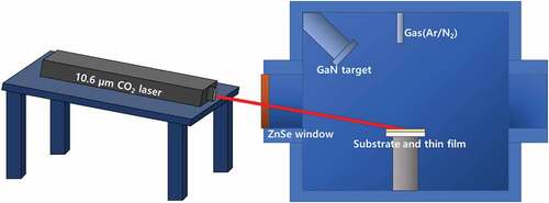
A CO2 laser-assisted RF sputtering process was used to deposit GaN thin films on sapphire substrates. A pre-sputtering process was performed to clean the target and sapphire (c-plane) substrate. To supply sufficient energy during thin-film growth for GaN wide bandgap materials, a CO2 laser (wavelength of 10,600 nm, beam diameter of 3.8 mm) was used to irradiate the substrate during RF sputtering. Irradiated optical energy can promote thin-film growth with sputtered adatoms in the substrate. A schematic of the CO2 laser-assisted RF sputtering system used in this study is shown in . A ZnSe single-crystal viewport was employed to transfer photon energy from the laser to the vacuum chamber in the sputtering system. The substrate temperature and working pressure during sputtering were 200°C and 15 mTorr, respectively. The processing energy, Ar partial pressure, and laser energy density during the CO2 laser assisted RF sputtering process ranged between 100 and 200 W, 20% and 80%, and 0 and 1.16 W/mm2, respectively. The crystal structure of the prepared GaN thin film was determined through XRD analysis, and New D8-Advance (Bruker-AXS) using CuKα radiation was analyzed under 40 kV and 40 mA conditions. The composition of the prepared thin film was determined through X-ray photoelectron spectroscopy (XPS) and analyzed using the AlKα line of K-alpha+ (Thermo Fisher Scientific). The transmittance was measured using a UV spectrometer Lambda 35 (Perkin Elmer), and a Tauc plot was used to extract the light energy bandgap through the transmittance value. The extracted energy bandgap was compared with the simulated energy bandgap measured by PL spectroscopy. Photoluminescence spectra were measured using a HeAg 30 Deep UV laser source at room temperature.
Figure 1. Schematic of the CO2 laser-assisted RF sputtering system.
3. Results and discussion
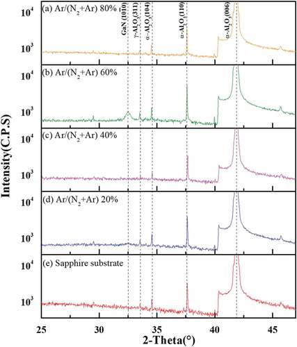
The X-ray diffraction patterns of the RF-sputtered GaN thin films fabricated by varying the Ar partial pressure are shown in . The RF sputtering process conditions were as follows: a substrate temperature of 200°C, RF power of 200 W, and working pressure of 15 mTorr. The Ar partial pressure was varied from 20% to 80% in 20% increments. The optimized partial pressure was considered and discussed to improve crystalline properties. As the Ar partial pressure increased to 60%, the (1010) peak of GaN was observed. The observed (1010) diffraction peaks of the RF-sputtered GaN thin films were attributed to the nonpolar planes of wurtzite GaN, which suggested the successful fabrication of the wurtzite GaN film. Black GaN films with poor crystallinity can be produced under low processing energy conditions during sputtering, which may result in the destruction of the atomic structure [Citation14]. However, the GaN thin films fabricated in this study were not black in color. The intensity of the (1010) diffraction peak related to the nonpolar plane showed the peak when the ratio of reactive gas N2 and inert gas Ar was properly mixed. The Ar-to-N2 gas ratio depends on the plasma density; thus, the Ar partial pressure in the plasma can affect the crystallinity of GaN thin films because the plasma quality is affected by the discharge current with Ar ions . This is consistent with previous reports stating that plasma density and discharge current increase with increasing Ar partial pressure [Citation21]. In , the GaN(1010) orientation diffraction peak (C.P.S) values were (a) 689, (b) 1030, (C) 722, (d) 709, and (e) sapphire substrate 688. Therefore, we confirmed that optimizing the Ar partial pressure during RF sputtering is an important step in the GaN thin-film process. The maximum intensity of the (1010) diffraction peak near 32° is observed at an Ar partial pressure of 60%.
Figure 2. X-ray diffraction patterns of the RF-sputtered GaN thin films deposited on sapphire substrates at the temperature of 200°C, RF power of 200 W, and working pressure of 15 mTorr, with different Ar partial pressure conditions (a) – (d) and without thin-film fabrication process (e).
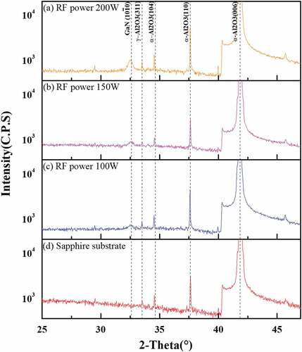
shows the X-ray diffraction patterns of the RF-sputtered GaN thin films fabricated under different RF power conditions. The generated power in the RF sputtering process was varied from 100 W to 200 W. Owing to the limitations of the RF power source, the generated output power was restricted to 200 W. The processing temperature, working pressure, and Ar partial pressure were 200°C, 15 mTorr, and 60% of Ar/(N2+ Ar), respectively. The intensity of the (1010) reflection peak increased with the increase in the applied RF power, indicating that a high energy is necessary to effectively grow GaN thin films through RF sputtering. A high RF power can help introduce high-quality plasma with high kinetic energy into the chamber during sputtering. Consequently, the high kinetic energy in the plasma can be transferred to the GaN thin films during fabrication.
Figure 3. X-ray diffraction patterns of the RF-sputtered GaN thin films deposited on sapphire substrates at the temperature of 200°C, working pressure of 15 mTorr, with different RF power conditions (a) – (c) and without thin-film fabrication process (d).
displays X-ray diffraction patterns of the CO2-laser-assisted RF-sputtered GaN thin films deposited on a sapphire substrate at a low temperature of 200°C. The laser energy density was varied from 0.44 W/mm2 to 1.16 W/mm2 in 0.18 W/mm2 increments. The CO2 laser with a wavelength of 10,600 nm employed to assist the RF-sputtering process has a photon energy to 0.12 eV. The intensity of the (0002) reflection of GaN significantly increased as the laser energy density increased from 0.8 W/mm2 to 0.98 W/mm2. At a laser energy density of 0.98 W/mm2, the (0002) peak of GaN was the dominant single film peak. The surface energy of the (0002) plane was higher than those of the other planes of wurtzite GaN, [Citation22] indicating that the required nucleation energy of the c-plane of the GaN thin films was the highest among those of the other planes. By employing the CO2 laser for RF sputtering, the fabricated GaN thin films were able to acquire sufficient nucleation and growth energies during the CO2 laser-assisted RF sputtering because the CO2 laser could supply sufficient formation energy density at the CO2 laser energy density of 0.98 W/mm2. In comparing the fabrication CO2 laser energy densities, the peak intensities of (1010) and (1011) were found to be lower under the energy density conditions of 0.62 and 0.8 W/mm2 compared with that at 0.98 W/mm2. This finding indicates that a CO2 laser energy density of 0.98 W/mm2 can supply sufficient energy for the nucleation and growth of reflections of the (0002) plane of GaN.
Figure 4. X-ray diffraction patterns of the CO2-laser-assisted RF-sputtered GaN thin films deposited on a sapphire substrate by varying the energy density of the CO2 laser. Process conditions: Ar partial pressure 60%, RF power 200 W, working pressure 15 mTorr, and substrate temperature 200°C (a) – (e). GaN thin film without CO2 laser assistance (f) and without thin-film fabrication process (g).
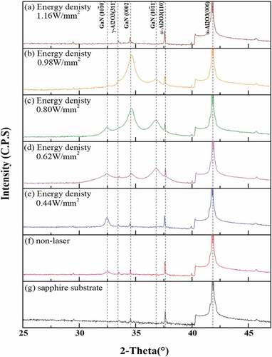
The peak intensity of the (1010) plane of GaN showed similar values up to a laser energy density of 0.8 W/mm2. However, as the laser energy surpassed 0.98 W/mm2, the (1010) peak of GaN suddenly disappeared, and the (0002) peak of GaN was formed. In addition, the XRD profiles of the sapphire substrate (non-laser) (f) and CO2-laser-assisted RF-sputtered GaN thin film fabricated at a laser energy density of 1.16 W/mm2 (a) were similar to those of an undeposited sapphire substrate. At a laser energy density of 1.16 W/mm2, the high laser energy density re-evaporated the GaN thin films on sapphire substrates. To estimate the surface energy of the (0002) plane of the GaN thin film, the Gibbs free energy per unit volume of the GaN thin films can be calculated using the following Equationequation (1)(1)
(1)
where γvf is the surface energy of the nucleus–substrate and ΔGv is the Gibbs free energy per unit volume of the solid phase. Further, θ is the contact angle at the thin film–substrate interface, which is equal to 180° for unattached thin films [Citation23]. Owing to the wurtzite structure of GaN, γvf depends on the direction of the plane. The surface energies of GaN semiconductors with wurtzite structures are summarized in . The surface energies of the (1010), (1011), and (0002) planes of the fabricated GaN thin films are 1.40, 1.76, and 2.64 J/m2 respectively [Citation22]. The GaN (0002) surface energy was about 2.64 J/m2, which means that the growth of the (0002) orientation reached the highest surface energy. As shown in , the GaN (0002) diffraction peak is the highest at a laser energy density of 0.98 W/mm2.
Table 2. Surface energy of the (0001), (1120), (1011), and (1010) planes of GaN wurtzite.
shows the (0002), (1010), and (1011) plane peak ratios according to the laser energy density calculated by EquationEquation (2)(2)
(2) [Citation24].
Figure 5. X-ray diffraction pattern peak ratios in (0002), (1010) and (1011) orientations of CO2 laser-assisted RF sputtered GaN thin films fabricated at different laser energy densities.
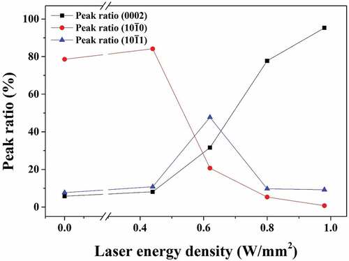
The peak ratio of the (1010) plane with the lowest surface energy was calculated to be 84% at a laser energy density of 0.44 W/mm2. At a laser energy density of 0.62 W/mm2, the peak ratio of the (1010) planes increased to 47%, and the peak ratio of the (0002) planes with the highest surface energy increased to 31.5%. At a laser energy density of 0.80 W/mm2, the peak ratio of (0002) planes increased to 77.7%, and the peak ratio of (1010) and (1011) planes with relatively low surface energy decreased. At a laser energy density of 0.98 W/mm2, the peak ratio of (0002) plane is 95.2%, indicating that most of the grains grow in (0002) orientation. As a result, this figure showed that higher peaks of (0002), (1011), and (1010) were observed at laser energy density of 0.98, 0.62, 0.44 W/mm2, respectively. It means that the required energies for (0002), (1011), and (1010) planes were well coincide with estimated surface energy in .
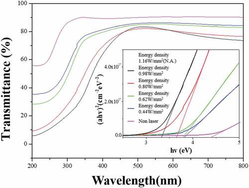
The optical transmission spectra of the CO2-laser-assisted RF-sputtered GaN thin films fabricated at different laser energy densities in the wavelength range of 200–800 nm are shown in . By increasing the CO2 laser energy density, the transmittance decreased from 90% to 80% within the wavelengths range near 500 nm. In addition, the wavelength edge of the transmittance increased from 267 nm to 345 nm with the increase in the CO2 laser energy density. Therefore, the estimated energy bandgap of CO2 laser-assisted RF-sputtered GaN thin films shifted to lower values at approximately 3.32 eV as the CO2 laser energy increased. The black line in corresponds to the CO2-laser-assisted RF-sputtered GaN thin film fabricated at a laser energy density of 0.98 W/mm2. For the laser energy density of 1.16 W/mm2, the transmittance value was not obtained. Apparently, the thin films evaporated during deposition, indicating that the increasing laser energy density aided the crystal growth of wurtzite GaN. The simulated data of the energy band gap from the Tauc plots of the CO2-laser-assisted RF-sputtered GaN thin films are presented in the insets of . The transmittance of the GaN thin films was measured using a UV-vis spectrometer, and the (ahν)2 vs. hν curve was subsequently plotted: [Citation25]
Figure 6. Transmittance and Tauc plot of the CO2 laser-assisted RF-sputtered GaN thin films fabricated at different laser energy densities. The insert shows the simulated bandgaps of the GaN thin films from the transmittance values.
where is the absorption coefficient,
is the optical bandgap of the GaN thin film, hν is photon energy, and A is a constant.
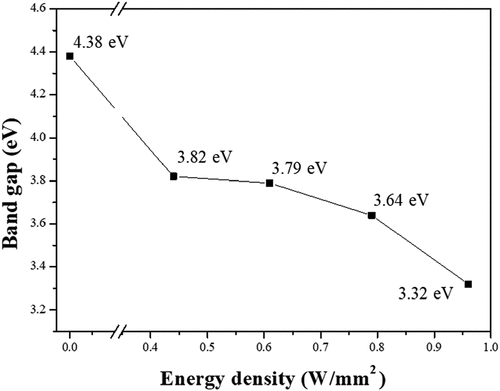
The relationship between the laser energy density and bandgap of the CO2-laser-assisted RF-sputtered GaN thin films is illustrated in . The energy bandgap decreased with increasing laser energy density. When the laser energy density approached 0.98 W/mm2, the energy bandgap of the CO2 laser-assisted RF-sputtered GaN thin films was 3.32 eV, which was similar to the reported bandgap of GaN thin films. When the laser energy density exceeded 1.14 W/mm2, delamination and re-evaporation of the GaN thin film occurred owing to the excessively high energy density of the CO2 laser. Therefore, the optimized photon energy of 0.98 W/mm2 can enhance the crystalline properties of the GaN thin film along the c-plane. Hence, CO2-laser-assisted RF sputtering is an effective method for growing GaN thin films.
Figure 7. Bandgaps of the CO2 laser-assisted RF-sputtered GaN thin films fabricated at different laser energy densities.
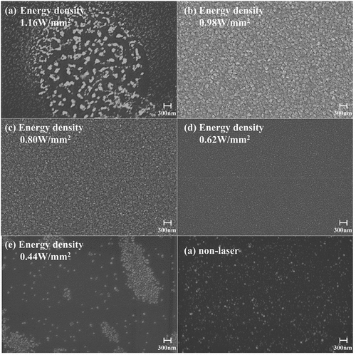
shows the SEM surface images of the CO2 laser-assisted RF-sputtered GaN thin films fabricated at different laser energy densities ranging from 0 W/mm2 to 1.16 W/mm2. In the SEM images of GaN thin films without laser (f) and with CO2 laser assistance with small energy density of 0.44 W/mm2 (e), a partially grown grain structure was observed. As the laser energy density was increased beyond 0.44 W/mm2, highly dense grains with a uniform size were formed. When the CO2 laser energy density approached 0.8 and 0.98 W/mm2, the grain size further increased. GaN thin films (b) deposited at a CO2 laser energy density of 0.98 W/mm2 were well crystallized in their thin film form. Therefore, CO2 laser-assisted RF-sputtered GaN thin films fabricated at a laser energy density between 0.8 and 0.98 W/mm2 exhibited relatively large grains and a uniform structure. Moreover, we determined that the grain size increased with increasing laser energy density. Finally, the partially damaged surface of the CO2 laser-assisted RF-sputtered GaN thin films fabricated at a high incident laser energy density of 1.14 W/mm2 () suggested that high laser energy densities can damage the thin film quality of the fabricated GaN [Citation26].
Figure 8. Scanning electron microscopy (SEM) images of the CO2 laser-assisted RF-sputtered GaN thin films fabricated at different laser energy densities.
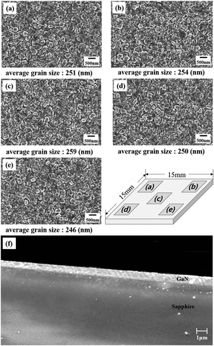
In , the average grain size of the central region of the GaN thin film was 259 nm, and the average grain size of the edge region was 246–254 nm. The average grain size of the whole thin film was 252 nm, indicating that the film quality in the central region and the edge region was almost uniform. In , the deposited GaN thin film is growing in the C-axis direction, and the thickness of the thin film has grown around 1 μm. It means that crystalline size of vertically grown grains (c-axis direction) were much larger than horizontally grown grains. In the experiments of X-ray photoelectron (XPS) and photoluminescence (PL) spectroscopy, and UV-vis spectrometry, a 1 μm-thick thin film was used.
Figure 9. Scanning electron microscopy (SEM) surface images (a)-(e), cross-sectional images (f) of CO2 laser-assisted RF sputtered GaN thin films fabricated at a laser energy density of 0.98 W/mm2.
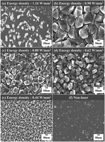
shows high-resolution SEM surface images of CO2 laser-assisted RF sputtered GaN thin films fabricated at different laser energy densities. In the GaN thin film (f) fabricated without laser assistance, small and non-uniformly grown crystal grains were observed. The GaN thin film fabricated with the assistance of a CO2 laser formed high-density particles at a laser energy density of 0.44 W/mm2. As a result of measuring the grain size of the GaN thin film fabricated with the assistance of a CO2 laser, (e): 41 nm, (d): 68 nm, (c): 122 nm, (b): 247 nm. shows the surface damaged by the high laser energy density. It shows that grain size increases with increasing laser energy density in the range 0–0.98 W/mm2. The optimal laser energy for obtaining a large grain size and high-density GaN thin film is 0.98 W/mm2.
Figure 10. High-resolution scanning electron microscopy (SEM) images of the CO2 laser-assisted RF sputtered GaN thin films fabricated at different laser energy densities.
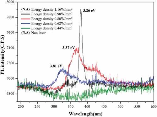
displays the PL spectra of the CO2 laser assisted RF-sputtered GaN thin films with different laser energy densities. In the PL measurement, a He-Ag source with UV laser system of 224 nm wavelength was employed as the excitation source, and a charge coupled device detector was used to record the PL data from the excited electron emission. In general, the PL peak of GaN is located at approximately 360–380 nm [Citation29,Citation30]. By varying the CO2 laser energy density from 0.62 W/mm2 to 0.98 W/mm2, the PL peak position shifted from 325 nm to 380 nm, which corresponded to 3.81 and 3.26 eV, respectively. These PL data show similar energy bandgap behavior in . When high laser energy densities of approximately 0.98 W/mm2 were applied in the thin film fabrication process, GaN thin film exhibited appropriate PL spectra at 3.26 eV. This PL spectrum value corresponds to the reported energy band gap of GaN thin films [Citation27,Citation28]. When a low energy density of approximately 0.44 W/mm2 or higher energy density exceeding 1.16 W/mm2 was applied, thin films showed no PL spectra peaks within the range of 325–380 nm. An appropriate energy density of the CO2 laser can promote the formation of the wurtzite GaN structure with energy band gap of 3.3–3.4 eV. Without CO2 laser assistance, the GaN structure was not properly formed, as evidenced by the absence of PL data near the 360–380 nm range.
Figure 11. Photoluminescence (PL) wavelength of the CO2 laser-assisted RF-sputtered GaN thin films fabricated at different laser energy densities.
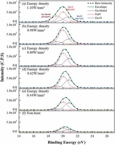
shows the XPS spectra of the Ga 3d core level of the CO2 laser-assisted RF-sputtered GaN thin films at different laser energy densities from 0.44 W/mm2 to 1.16 W/mm2 and films RF-sputtered without CO2 laser assistance. Without CO2 laser assistance, the Ga 3d core level showed a faint peak intensity, meaning that the GaN thin film was hardly formed during RF sputtering. However, by introducing CO2 laser irradiation during RF sputtering, the Ga 3d core level showed increased peak intensity. The envelope, Ga 3d core level peak comprised three peaks originating from Ga-N, Ga-metal, and Ga-O bonds, which corresponded to 19.9, 19.0, and 20.7 eV, respectively [Citation27]. As shown in the , by increasing the laser energy density from 0.44 W/mm2 to 0.98 W/mm2, the number of Ga-N bonds increased, while those of Ga-metal and Ga-O were virtually unchanged. This finding means that near the laser energy density of 0.98 W/mm2, the GaN thin film grew properly. However, as the laser energy density was increased to 1.16 W/mm2 (), the peak intensity of Ga-N bonds decreased. As previously discussed, the GaN structure can be destroyed by high laser energy densities. As shown in the , the envelope peak center shifted to low energy level with increasing laser energy density due to the increased number of G-N bonds at the energy density of 0.98 W/mm2. At the assisted CO2 laser energy density of approximately 0.98 W/mm2, the Ga 3d core level showed the highest envelope intensity and Ga-N binding energy. This finding means that at the laser energy density of 0.98 W/mm2, GaN thin film has the highest number of Ga-N bonds and a well-grown crystalline structure.
Figure 12. X-ray photoelectron spectroscopy (XPS) spectra of the Ga 3d core level of the CO2 laser-assisted RF-sputtered GaN thin films deposited on a sapphire substrate by varying the energy density of the CO2 laser. Process conditions: Ar partial pressure 60%, RF power 200 W, working pressure 15 mTorr, substrate temperature 200°C.
4. Conclusion
For the first time, CO2 laser-assisted RF-sputtered GaN thin films were prepared by varying the laser energy density at a relatively low substrate temperature of approximately 200°C. To assist in the growth of crystallized GaN thin films on sapphire substrates, a CO2 laser was employed during the RF sputtering process. By employing CO2 laser with energy density of 0.98 W/mm2 to assist RF sputtering at a low substrate temperature of 200°C, (0002) oriented, well-grown crystalline-structured GaN thin films were obtained. Both the measurement methods of Tauc plot and PL spectra proved that GaN thin films processed with the CO2 laser and RF sputtering system yielded a well-grown (0002) orientation with a wide energy bandgap of 3.26 eV when the CO2 laser was irradiated at an energy density of 0.98 W/mm2 during the RF sputtering process.
Disclosure statement
No potential conflict of interest was reported by the author(s).
Additional information
Funding
References
- Sichel EK, Pankove JI. Thermal conductivity of GaN, 25-360K. J Phys Chem Solids. 1977;38:330.
- Kim M, Seo J, Singietti U, et al. Recent advances in free-standing single crystalline wide band-gap semiconductors and their applications: gaN, SiC, ZnO, β -Ga2O3, and diamond. J Mater Chem C. 2017;5:8338.
- Chow T. High-voltage SiC and GaN power devices. Microelectron Eng. 2006;83:112–122.
- Shchekin O, Epler J, Trottier T, et al. High performance thin-film flip-chip InGaN–GaN light-emitting diodes. J Appl Phys Lett. 2006;89:071109.
- Uemoto Y, Hikita M, Ueno H, et al., Gate Injection Transistor (GIT)—A normally-off AlGaN/GaN power transistor using conductivity modulation. IEEE Trans Electron Devices. 2007;54:12.
- Jogai B. Influence of surface states on the two-dimensional electron gas in AlGaN/GaN heterojunction field-effect transistors. J Appl Phys. 2003;93:3.
- Osipov K, Ina Ostermay I, Bodduluri M, et al., Local 2DEG density control in heterostructures of piezoelectric materials and its application in GaN HEMT fabrication technology. IEEE Trans Electron Devices. 2018, 65, 8.
- Dissanayake A, Lin JY, Jiang HX, et al. Low temperature epitaxial growth and photoluminescence characterization of GaN. J Appl Phys Lett. 1994;65:2317.
- Richter E, Gramlich S, Klein A, et al. Direct growth of GaN on (0001) sapphire. J Phys Stat Sol. 2001;188:439.
- Lee JW, Paek HS, BYoo J, et al. Low temperature buffer growth to improve hydride vapor phase epitaxy of GaN. J Mater Sci Eng. 1999;59:12.
- Huang TF, Marshall A, Spruytte S, et al. Optical and structural properties of epitaxial GaN films grown by pulsed laser deposition. J Cryst Growth. 1999;200:362.
- Kawwam M, Lebbou K. The influence of deposition parameters on the structural quality of PLD-grown GaN/sapphire thin films. J Appl Surf Sci. 2014;292:906.
- Li W, Li A. Post growth thermal annealing of GaN grown by RF plasma MBE. J Cryst Growth. 2001;227:415.
- Maruyama T, Miyake H. Gallium nitride thin films deposited by radio-frequency magnetron sputtering. J Vac Sci Technol A. 2006;24:1096.
- Yadav BS, Singh S, Ganguli T, et al. Highly oriented GaN films grown on ZnO buffer layer over quartz substrates by reactive sputtering of GaAs target. Thin Solid Films. 2008;517:488–493.
- Nisha Preschilla A, Major S. Nanocrystalline gallium nitride thin films. Appl Phys Lett. 2000;77:1861.
- Kikuma T, Tominaga K, Furutani K, et al. GaN films deposited by planar magnetron sputtering. Vacuum. 2002;66:233–237.
- Shinoda H, Mutsukura N. Structural properties of GaN and related alloys grown by radio frequency magnetron sputter epitaxy. Thin Solid Films. 2008;516:2837–2842.
- Naniwae K, Itoh S, Amano H, et al. Growth of single crystal GaN substrate using hydride vapor phase epitaxy. J Cryst Growth. 1990;99:1–4.
- Pearton SJ, Ren F, Zhang AP, et al. Fabrication and performance of GaN electronic devices. Mater Sci Eng R Rep. 2000;30:3–6.
- Borah SM, Bailung H, Pal AR, et al. Study on the influence of nitrogen on titanium nitride in a dc post magnetron sputtering plasma system. J Phys D: App Phys. 2008;41:195205.9.
- Hong YJ, Yoo J, Doh YJ, et al. Controlled epitaxial growth modes of ZnO nanostructures using different substrate crystal planes. J Mater Chem. 2009;19:941–947.
- Cao G Nanostructures & nanomaterials: synthesis, properties & applications. Imperial college press, 2004. 93p.
- Jin SD, Koh J-H. Effects of calcination temperature on the piezoelectric properties of lead-free Ag doped (Na, K) NbO3–LiTaO3 piezoelectric ceramics. J Alloys Compd. 2013;555:390–394.
- Lin K, Kuo DH. Characterization of quaternary AlInGaN films obtained by incorporating Al into InGaN film with the RF reactive magnetron sputtering technology. J Mater Sci: Mater Electron. 2017;28:43–51.
- Yoo JH, Menor MG, Adams JJ, et al. Laser damage mechanisms in conductive widegap semiconductor films. Opt Express. 2016;24:16.
- Kumar M, Pasha SK, Krishna TC, et al. Facile synthesis and photoluminescence spectroscopy of 3D-triangular GaN nano prism islands. J Dalton Trans. 2014;43:11855.
- Kim D, Song KM, Jung U, et al. Effects of different InGaN/GaN electron emission layers/interlayers on performance of a UV-A LED. Appl Sci. 2020.10.1514.
- Wu S, Wang L, Yi X, et al. Influence of lateral growth on the optical properties of GaN nanowires grown by hydride vapor phase epitaxy. J Appl Phys. 2017;20:122.
- Jiao W, Kong W, Li J, et al. Characterization of MBE-grown InAlN/GaN heterostructure valence band offsets with varying In composition. J AIP Adv. 2015;6:3.