
 ?Mathematical formulae have been encoded as MathML and are displayed in this HTML version using MathJax in order to improve their display. Uncheck the box to turn MathJax off. This feature requires Javascript. Click on a formula to zoom.
ABSTRACT
Binary sulfides were deposited by sequential thermal evaporation with the stacking order glass/CuS/SnS/ZnS and subsequently subjected to a sulfurization-crystallization process, considering two thermal treatment time intervals, 5 and 20 min. The objective of implementing different annealing durations was to identify the best conditions to form CZTS films in the pure kesterite phase. After being subjected to the annealing, the films show structural characteristics of the kesterite phase. However, XRD data showed that prolonged annealing causes degradation of the kesterite phase, leading to the formation of traces of CuS and Cu5Sn2S7. The films annealed for shorter duration, in this case 5 min, present a denser and more uniform surface morphology, better degree of preferential orientation, small Urbach energy of 0.302 eV, and higher photosensitivity. The band gap of the films was 1.46 eV and 1.53 eV for annealing durations 5 and 20 min, respectively.
Graphical abstract
1. Introduction
The search of absorber materials for photovoltaic devices using elements with low toxicity, and abundance in the earth’s crust has accelerated in recent years. Materials with kesterite structure such as Cu2ZnSnS4 (CZTS), Cu2ZnSnSe4 (CZTSe) and the mixed chalcogenide Cu2ZnSn(S/Se)4 (CZTS/Se) have presented a strong interest as a substitute for CIGS and CdTe absorber layers [Citation1]. However, CZTS is considered a better option because the constituent elements Cu: 68 ppm, Zn: 79 ppm, Sn: 2.2 ppm and S: 420 ppm are abundant in the earth’s crust, and, apart from inexpensive they are nontoxic [Citation2]. CZTS exhibits a direct band gap in the range 1.4 eV – 1.6 eV [Citation3] and a large absorption coefficient (~ 104 cm−1) [Citation4], making it an excellent candidate for use as an absorber in thin-film solar cells. In addition, it shows great potential for application in photodetection [Citation5], gas detection [Citation6], electrodes for water splitting [Citation7], energy storage, humidity sensors, thermoelectric, CO2 reduction, and smart devices [Citation8]. CZTS can exist in two crystal structures, specifically Kesterite (space group ) and Stannite (space group
) [Citation9]. Of these, kesterite has a stable structure, as its formation energy is lower than stannite [Citation10]. Although the CZTS semiconductor is very promising due to the above mentioned aspects, further studies and material optimization are needed to reach the theoretically achievable efficiency of CZTS-based devices which is higher than 30% [Citation11]. The current power conversion efficiency (PCE) record of Cu2ZnSn(S,Se)4 based devices is 13.5% [Citation12]. In the quest to achieve photovoltaic grade CZTS material, different deposition techniques have been implemented. Usually, the CZTS growth process is achieved in two stages. The first stage consists of the deposition of precursors such as Cu, Zn, Sn, SnS, ZnS, CuS using vacuum-based methods [Citation13–15] or chemical (non-vacuum) processes [Citation16–18]. The second stage consists of the annealing/sulfurization of the deposited precursor film stack. Among the various deposition techniques, vacuum evaporation has emerged as an easy-to-use technique and has proven to be a commercially scalable and cost-effective method for the growth of high-quality and reproducible thin films. However, obtaining the CZTS film in its pure phase remains a challenge that requires further understanding. Research related to the formation of CZTS highlights the need to optimize the different growth/processing parameters such as the elemental proportion of the precursor [Citation11], thickness of the precursor layers, temperature ramp rate during annealing and the recrystallization temperature, sulfurization time, etc [Citation19]. Identifying and optimizing the formation conditions to obtain phase-pure CZTS is of primary importance since small deviations in its stoichiometry introduce unwanted secondary and ternary phases that can change the properties of CZTS [Citation8]. There are reports that CZTS films thermally treated below 525℃ has the binary and ternary phases such as SnS, ZnS, CuS, Cu8S5, Cu3SnS4, Cu2SnS3 [Citation20,Citation21]. Likewise, there are indications that the stacking order of the precursor layers influence the kesterite phase. When the stacking order is glass/SnS2/Cu/ZnS or glass/Cu/ZnS/SnS2, the final kesterite product is accompanied with traces of Cu2-x, SnS2 and SnS as secondary phase, however, the stacking order glass/ZnS/SnS2/Cu resulted in better kesterite material [Citation22]. The glass/CuSn/Zn/Cu and glass/CuSn/ZnS/Cu stacking order, subjected to a very short period of sulfurization (500℃ and 525℃) shows diffraction peaks of kesterite phase accompanied by Cu-S/SnS-based secondary phases. However, the glass/CuSn/ZnS/Cu stacking order where the layers are deposited by sputtering and a subsequent sulfurization at 550°C for 1 min presents more promising results in terms of crystal quality and optical properties [Citation11]. Similarly, the glass/Cu/SnS/ZnS/Cu and glass/Cu/SnS/Zn/Cu stacking order, subjected to a period of sulfurization for 1 min. It was observed that the sample prepared using binary ZnS layer stack (Cu/SnS/ZnS/Cu) reacted at 525℃ presented more promising results for solar cell applications [Citation23]. Singh et al. obtained CZTS films with preferential growth along the (112) plane and optical band gap 1.42 eV by sequential sputtering from the metal targets Cu:Sn, Sn, and Zn followed by a thermal treatment at 550℃ for 12 min [Citation24]. The stacking order of the layers were glass/Cu:Sn/Sn/Zn. Likewise, Fan et al. obtained CZTS thin films by the sequential evaporation of Zn, Cu, and Sn, followed by a sulfurization process at 500℃ for different time durations in the range 30–120 min. It was observed that the annealing duration of 90 min resulted phase-pure CZTS films with better crystalline quality [Citation25]. Treatment durations less or greater than 90 min lead to incomplete recrystallization and formation of secondary phases, respectively. There are plenty of reports in the literature on CZTS devices where the absorber films were deposited by different techniques, to mention few: we have previously reported Ge doped CZTS devices fabricated by sequential sputtering of the glass/Cu/Sn/Cu/Zn metallic stacks followed by sulfurization, achieving 7% efficiency [Citation26]. A thin layer of Ge with varying the stacking order has been studied and the best results were obtained with a 5 nm Ge layer at the top of the metallic stack. Nguyen et al. used CZTS nanoparticles synthesized by hot-injection method to prepare the printing ink, obtaining ≈5% efficiency after annealing the CZTS films in Se vapor forming CZTSSe [Citation27]. Erkan et al. reported that the use of graphene as an inter-layer in CZTS cell structure enhanced the conversion efficiency from 2.40% to 3.52% due to improvement of crystalline quality of the absorber layer. The CZTS thin film was deposited onto the glass/Mo/graphene structure using a single sputtering target [Citation28]. It is well established that the kesterite with Se (CZTS/Se) has superior performs than the counterpart without Se (CZTS). An efficiency of 13.5% has been reported recently for the CZTSSe [Citation12], while the highest efficiency of CZTS is 8.7% [Citation8]. Independent of the film deposition method or the initial precursor, a post-deposition thermal processing in presence of S or Se vapor, depending on the absorber, is required to obtain good device performance. The temperature, annealing duration, ambient, amount of S or Se, etc., is critical to obtain phase-pure kesterite with superior opto-electronic characteristics.
Although CZTS films have been developed by different methods including the sequential deposition of metal precursors, few studies discuss the sequential deposition of binary sulfides and their thermal processing/sulfurization. In this work, we report the post-deposition thermal processing of CZTS films obtained by vacuum evaporation of three binary sulfides: CuS, SnS, and ZnS. The binary layers were previously developed in our group in the stacking order glass/CuS/SnS/ZnS [Citation21]. The freshly deposited stacks were subjected to a sulfurization-recrystallization process at 550℃ for different time durations in an Ar + S atmosphere. The main objective of this research was to explore the influence of sulfurization-crystallization process on the structural, morphological, and optical properties of the resulting CZTS film and identify the conditions that improve the crystalline quality and optoelectronic properties of the CZTS film.
2. Methodology
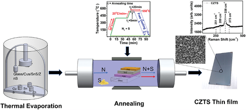
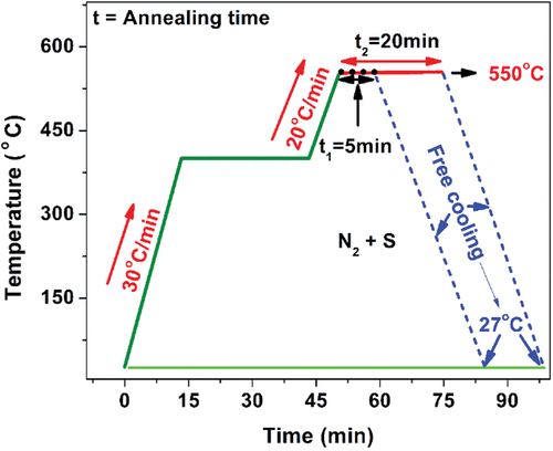
CZTS films were deposited on Corning glass substrates by sequential evaporation of the binary sulfides in the following order, glass/CuS/SnS/ZnS. These sulfides CuS (99%), SnS (99%) and ZnS (99%) were provided by Sigma Aldrich. During deposition, the vacuum was maintained at 1 × 10⁻⁵ Torr and the deposition rate was controlled by a digital quartz crystal monitor. The thicknesses of CuS, SnS and ZnS were 260 nm, 320 nm, and 50 nm, respectively. In a tube furnace (Thermoline model 21,100) equipped with Eurotherm 2116 temperature control, the stack of binary compounds was subjected to the sulfurization-crystallization process. Under an atmosphere of Ar + S (5 mg) at a pressure of 1 Torr, the furnace temperature was gradually increased until the maximum sulfurization temperature of 550℃ was reached. This temperature was kept constant in both 5 min and 20 min annealing. After the annealing, the system was cooled down naturally. The temperature versus time profile used in this study is shown in .
Figure 1. Temperature vs. time profile used in the sulfurization-crystallization process.
The structural properties of the films were determined with a Rigaku X-ray diffractometer, model SmartLab. X-ray spectra were obtained using Cu radiation (K = 1.54056 Å) in the 2θ range 15° – 80° at a grazing angle of 1°. Raman spectra were recorded using a Horiba Jobin Yvon LabRam HR spectrophotometer using 514 nm laser excitation source. The morphology of the films was studied with a JEOL model JSM-7100 F scanning electron microscope (SEM). The elemental composition of the films was determined by energy-dispersive X-ray spectroscopy (EDXS) using a Hitachi Su I510 SEM. The roughness of the films was observed with a VEECO atomic force microscope (AFM) in contact mode, and the images were analyzed with NanoScope Analysis 1.5 software. The optical transmittance of the films was recorded in the wavelength range of 400–1100 nm using a Shimadzu UV-VIS-NIR spectrophotometer UV-3101PC. For photo response measurement, two carbon electrodes were placed on the surface of the films in a coplanar configuration. The light source was an 80 mW/cm2 incandescent tungsten halogen lamp. Under a constant potential of 1 V, the current was measured for 30s; starting with 10s in the dark, followed by 10 s under illumination and finally 10 s in the dark. A Keithley 230 voltage source and a Keithley 619 electrometer were used for data recording.
3. Results and discussion
3.1. Structural analysis
shows the XRD patterns of films grown by CuS – SnS – ZnS stacking, (a) without heat treatment, and heat treated at 550℃ for (b) 5 min, and (c) 20 min in an Ar + S atmosphere. The XRD patterns of the as-deposited stack () can be indexed according to the binary phases SnS (PDf 39-0354), ZnS (PDF 05-0566) and CuS (PDF 06-0404). shows that the applied heat treatments facilitate crystallization. For a heat treatment time of 5 min, more defined and intense peaks are observed, indicating better crystallization. Intensity of XRD patterns corresponding to CuS, ZnS and SnS phases decrease while the intensity of the kesterite phase, identified by the reflections from the (200), (220), (312), (224), (008), (332) planes intensifies with a strong preferential orientation in the (112) plane. As a reference, the patterns of the CZTS with tetragonal phase (PDF 26–0575) are also included in . In addition, the appearance of a low-intensity peak belonging to SnS can be observed. However, upon increasing the annealing duration to 20 min, the low-intensity band of the SnS (PDF 39–0354) grow intense, and a new XRD peak belonging to Cu5Sn2S7 (PDF 40–0924) is observed. Further, a decrease in intensity of the reflections corresponding to the kesterite phase in evident (). The values of lattice parameters are a good indicator of the lattice distortions, comparing with the lattice values a = 5.427 Å and c = 10.848 Å of the CZTS reference (PDF 26–0575), the film annealed for 20 min show slight variations in the lattice constant. However, the obtained results show c/2a values close to one, indicating that the unit cell of the annealed films is of tetragonal type [Citation29].
Figure 2. XRD patterns of CZTS thin films. a) as deposited, and sulfurised in Ar + S ambient at 550°C for b) 5 min, and c) 20 min. Standard powder diffraction patterns of Cu2ZnSnS4 (PDF # 26–0575) are shown in d).
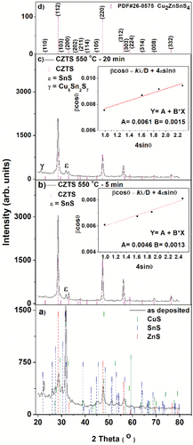
The crystallite size was calculated using the Scherrer formula D = (κλ/βcosθ) for the diffraction peak (112) [Citation11]. In addition to the crystal size (D), the microstrain (ε) and dislocation density (δ) were calculated using the Williamson and Hall (W-H) approximation (Eq. 1 & Equation2(2)
(2) ):
βcosθ = (κλ/D) + 4εsinθ (1)
Where β is full width at half maximum, κ is a constant (κ = 0.94), λ is the wavelength of the incident CuKα X-ray radiation. D and ε were calculated from the intercept and slope of the plot βcosθ vs 4εsinθ, which is shown in the inset of .
The crystallite size decreases from 31.0 nm to 23.3 nm as the annealing duration increases (). Lattice defects are known to facilitate dislocations in the crystals and increase the dislocation density, which in turn results in increased microstrain, which is detrimental to crystal growth [Citation30]. In the present case, microstrain and dislocation density are higher for longer annealing duration, indicating an increase in point defects. Consequently, as can be seen in , the film annealed for short duration shows larger crystal size, minimizing the imperfections in the crystal lattice. This leads to a reduction of the microstrain and dislocation density in the film.
Table 1. Lattice parameter, crystal size measured by Scherrer and Williamson–Hall method, deformation, and degree of preferential orientation of the sulfide films annealed in Ar + S at 550°C for 5 and 20 min. In all cases, a fixed amount of sulfur (5 mg) was used.
The degree of preferential orientation (σ) for each of the films treated for different periods of time was calculated using EquationEquation (3)(3)
(3) .
Where Pi is the texture coefficient of plane i, and Pio is the texture coefficient of the powder sample, which is always unity and N is the number of X-ray peaks used for the analysis. As can be seen in , as the annealing time increases, there is an increase in the SnS phase and the appearance of the Cu5Sn2S7 phase due to the decomposition of CZTS. This can be a possible reason for the observed changes in the degree of preferential orientation and crystal size, as can be seen in .
. Lattice parameter, crystal size measured by Scherrer and Williamson–Hall method, deformation, and degree of preferential orientation of the sulfide films annealed in Ar + S at 550°C for 5 and 20 min. In all cases, a fixed amount of sulfur (5 mg) was used.
3.2. Raman analysis
Raman spectroscopic analysis was performed as a complementary method to confirm the formation of CZTS structure. CZTS reportedly shows Raman bands at 252 cm−1, (287 − 289) cm−1, (337–338) cm−1, 351 cm−1, (368, 372–374) cm−1 [Citation21,Citation31]. As expected, the as-grown film stack shows no evidence of CZTS structure, all the Raman bands coincide with the SnS and CuS binary phases reported at 289 cm−1, 222 cm−1 [Citation32] and 475 cm−1 [Citation33]. The band at 336 cm−1 () can be of CZTS or Cu2SnS3, however, given the fact that the stack is unannealed and the intensity of the band is lower (in CZTS it is the principal band), we assign it to Cu2SnS3 as reported [Citation34]. It was not possible to observe the ZnS phase under the 514 nm excitation, which requires an ultraviolet (UV) laser [Citation13]. The films thermally treated at 550℃ for 5 min and 20 min () show vibrational modes around 338 cm−1 and 289 cm−1 which are identified with the “A” symmetry modes of CZTS, as well as bands observed at 369 cm−1 and 372 cm−1 which coincides with the Raman bands of CZTS. On the other hand, the film annealed for 20 min () shows bands at 267 cm−1 and 351 cm−1 corresponding to the Cu2SnS3 ternary phase [Citation21,Citation33] and a shoulder band at 181 cm−1 corresponding to the SnS binary phase [Citation35]. The band at 245 cm−1 is not specific to the CZTS structure and does not coincide with the possible secondary or ternary phases, such as SnS2, CuS, ZnS, Cu3SnS4, and Cu2SnS3 [Citation31,Citation36]. The formation of this phase could be related to the stoichiometry change demonstrated in . In particular, the position and intensity of the Raman modes are dependent on the elemental composition and very sensitive to the presence of defects in the CZTS structure [Citation37].
Figure 3. Raman spectra of CZTS films. a) as-deposited, and sulfurised in Ar + S ambient at 550°C for b) 5 min and c) 20 min.
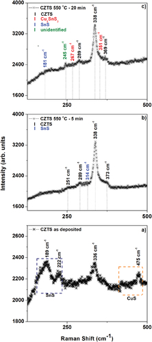
Table 2. Elemental composition (at %) of CZTS films annealed at 550℃ for different time durations.
3.3. Surface morphology and elemental composition
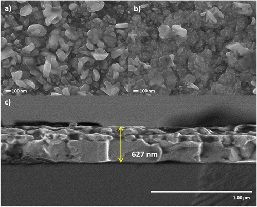
shows SEM images of the annealed films together with a cross section view of the film annealed for 5 min. Change in surface morphology when annealing duration increased from 5 min () to 20 min () is noticeable. Longer annealing resulted in the fragmentation of the grains and a non-uniform distribution of small agglomerated particles, which is probably associated with the change in material properties discussed above [Citation3,Citation16,Citation18]. The agglomerated particles with small bright spots could be attributed to the formation of SnS and Cu5Sn2S7 phases identified in XRD [Citation38]. While the film shown in presents a denser surface, and also based on the XRD and Raman data, we consider that 5 min annealing is appropriate. The 5 min annealed film show a thickness of 627 nm, which can be seen in the cross-section image in , the corresponding thickness of the film annealed for 20 min is 636 nm.
Figure 4. SEM images of the sulfurised CZTS thin films in Ar + S ambient at 550°C for a) 5 min and b) 20 min. c) shows the cross-section image of the film annealed for 5 min.
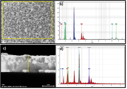
shows the EDXS scan results together with an image of the surface and cross section of the CZTS film from where the data were collected. The data corresponds to the film annealed for 5 min. As seen in , the atomic composition of the film annealed for 5 min is close to that of the ideal case (see values in brackets). However, the composition of the film annealed for 20 min is significantly deviated from the ideal stoichiometry. Deviations from the ideal stoichiometry favor the appearance of defects and secondary phases [Citation39]. The above observation can be is related to the increase of the SnS phase and the appearance of the Cu5Sn2S7 phase discussed in the XRD section. According to reports, the suitable composition ratio Cu/(Zn +Sn) for high-efficiency CZTS devices is between 0.80 and 0.90 and that of Zn/Sn is 1.1–1.3 [Citation40]. In particular, the film heat-treated for 5 min has the closest composition ratio Cu/(Zn+Sn) = 0.77 and Zn/Sn = 1.10.
Figure 5. A) Surface and c) cross-sectional EDXS analysis of a CZTS film heat-treated at 550℃ for 5 minutes, the rectangular region marked with yellow boundaries in (a) and the vertical line in (c) indicates the selected region of EDXS analysis. b) and d) are the EDXS spectra.
. Elemental composition (at %) of CZTS films annealed at 550℃ for different time durations.
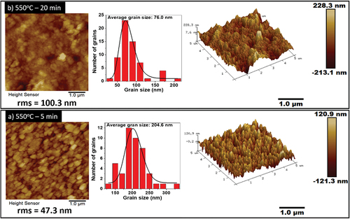
shows 2D and 3D atomic force microscopy micrographs of CZTS films measured over an area of 5 μm × 5 μm. A change in morphology is observed when the annealing duration is increased from 5 to 20 min. The corresponding histograms show the grain size distribution. The morphology reveals uniform grain size and shape in the case of 5 min annealing with a mean grain size 204.6 ± 3.9 nm (). However, with the increase in annealing time, a decrease in grain size to 76.0 ± 1.6 nm was observed (), which can be attributed to the degradation of the material forming SnS, CuS and the impurity phase Cu5Sn2S7 as revealed in the XRD patterns (), and Raman spectra (). The root mean square (rms) roughness of the film increased from 47.3 nm to 100.3 nm with increase in annealing duration. The increase in roughness could be due to the reduction of grain size and nonuniform surface.
Figure 6. AFM images of the CZTS films annealed for a) 5 min and b) 20 min.
3.4. Optoelectronic properties
The optical properties of the films heat-treated for different time durations were studied using the UV-Vis transmittance spectra in the range 400–1100 nm (inset of ). The band gap of the films was estimated from the Tauc plot using the formula for the direct transition, shown in EquationEq. (4)(4)
(4) . Where
is the absorption coefficient,
is the photon energy, c is a constant and
is the direct band gap [Citation41].
Figure 7. A) Graph of the optical absorption coefficient of CZTS films. The inset shows the transmittance (T%) of the films. b) Plot of for the band gap estimation. The inset shows the Urbach plot (
).The annealing times are shown in each plot.
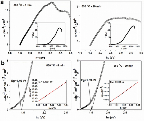
shows that the value of optical absorption coefficient is ~3x104 cm−1 at the onset of the band edge absorption, making it suitable for solar cell applications [Citation42]. Band gap of the film annealed for 5 min is 1.46 eV, however, it increased to 1.53 eV when the film is annealed for 20 min. This increase can be a result of the formation of binary and ternary phases discussed above. The structural disorder of CZTS manifests as Urbach tail, and hence Urbach energy can shed insight into the band gap states originating from disorder or defect states. In the EquationEq. (5)(5)
(5) [Citation29],
is the absorption coefficient,
is the photon energy and Eu is the Urbach energy.
The Urbach energy is obtained from the inverse of the slope of the linear part of the plot, as shown in the inset of . The estimated values of the Urbach energy are in the range of 0.3–0.4 eV. These values are within the range reported for CZTS films [Citation10,Citation43]. The Urbach energy of the film annealed for 5 min (0.302 eV) is lower than that of the film annealed for 20 min (0.398 eV). High Urbach energy values can be attributed to levels of impurities or defects introduced in the band structure during the prolonged annealing time [Citation44]. In general, highly crystalline semiconductors exhibit a few tens of meV for the Urbach energy [Citation45], below which there is a decrease in the density of localized states [Citation46].
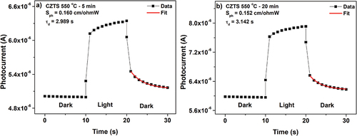
The photosensitivity of the CZTS films was evaluated from the photoresponse measurements, which is explained in section 2. shows the photocurrent curves of the CZTS films discussed in this work. The slow rising edge of the photoresponse and the much slower decaying edge after the illumination period indicates the presence of trapping levels in the band gap [Citation47].
Figure 8. Photocurrent response of CZTS thin films annealed at 550°C for time durations a) 5 min. and b) 20 min. The best fit to EquationEq. (6)(6)
(6) is represented with the red line, the photosensitivity
and the decay time (
are indicated in the figure.
The decay time was calculated by fitting the experimental data to EquationEq. (6)(6)
(6) [Citation6]:
Where Io is the initial current, A is an independent variable, and is the decay time. The film subjected to an annealing time of 5 min presented the lowest
(2.989 s), indicating a better quality material with fewer defects [Citation5]. With increasing annealing time, a larger value of
was registered (3.142 s), indicating more trap states [Citation48]. As discussed above (XRD and Raman), the film went through longer annealing durations has phase segregation and poor material quality.
The photosensitivity was calculated using the expression , where
and
are the conductivity in light and dark respectively, and Pinc is the incident power [Citation49]. The conductivity of the films increased with increasing annealing time (). The calculated photosensitivity for the films with 5 min and 20 min annealing time was 0.160 cm/ΩW and 0.152 cm/ΩW respectively. In the literature, the reported values of photosensitivity are in the range of 0.14–0.8 cm/ΩW ( and the references therein). The film with the shorter annealing time shows higher photosensitivity, which can be attributed to the larger crystallite size and phase-purity of the CZTS material as discussed in the XRD and Raman analysis. Further, the SEM and AFM images reveal larger grains for the short-duration annealed film, implying less grain boundaries, which reduces the recombination of photo-generated charge carriers [Citation50]. On the other hand, the lower photosensitivity of the film subjected to larger annealing duration can be a result of the phase segregation and possible increase in recombination centers [Citation51]. The dark and light conductivity, and photosensitivity of the films are shown in .
Table 3. Dark and light conductivity, and photosensitivity of the CZTS thin films annealed at 550°C for time durations 5 and 20 min.
. Dark and light conductivity, and photosensitivity of the CZTS thin films annealed at 550°C for time durations 5 and 20 min.
4. Conclusions
In this work, the role of annealing duration on the formation of CZTS film from the precursor layers staked in the order glass/CuS/SnS/ZnS, and the subsequent recrystallization has been studied by analyzing the structural, morphological, and optoelectronic data. It was found that longer annealing duration causes not only the grain fragmentation but also leads to phase segregation and deterioration of photosensitivity. The smaller grain size after longer annealing duration can be a result of secondary phases, which inhibit the grain growth. The difference in grain size, morphology, and the surface roughness of the films annealed for different time durations was remarkable. The film annealed for 5 min has a band gap of 1.46 eV and Urbach energy 0.302 eV, both lower than the corresponding values of the film annealed for longer duration. Based on the discussed results, we propose that annealing at 550℃ under Ar + S ambient for 5 min can result in phase-pure CZTS for further applications.
Acknowledgments
The authors acknowledge AFM, SEM and RAMAN facilities provided by IER-UNAM. The authors wish to thank Gildardo Casa Rubia Segura for AFM images, Ing. Rogelio Moran Elvira for SEM images and Rubi Sotelo Marquina for images RAMAN and general help in the Lab.
Disclosure statement
The authors declare that they have no known competing financial interests or personal relationships that could have appeared to influence the work reported in this paper.
References
- Balaji G, Balasundaraprabhu R, Prasanna S, et al. Investigations of RF magnetron sputtered CZTS absorber layer thin films prepared using sulfur induced binary targets without sulfurization. Opt Mater. 2018;75:56–60.
- Paranthaman MP, Wong-Ng W, Bhattacharya RN. Semiconductor materials for solar photovoltaic cells. Switzerland: Springer; 2016.
- Liu WS, Chen SY, Huang CS, et al. Investigation of Zn/Sn ratio for improving the material quality of CZTS thin films with the reduction of Cu2-xS secondary phase. J Alloys Compd. 2021;853:157237.
- Kaza J, Pasumarthi MR, Avadhani PS. Superstrate and substrate thin film configuration of CdS/CZTS solar cell fabricated using SILAR method. Opt Laser Technol. 2020;131:106413.
- Gour KS, Karade V, Pandey A, et al. High-speed, low-bias operated, broadband (Vis-NIR) photodetector based on sputtered Cu2ZnSn(S, Se)4 (CZTSSe) thin films. Sens Actuator A Phys. 2020;314:112231.
- Gour KS, Bhattacharyya B, Singh OP, et al. Nanostructured Cu2ZnSnS4 (CZTS) thin film for self-powered broadband photodetection. J Alloys Compd. 2018;735:285–290.
- Gour KS, Singh OP, Bhattacharyya B, et al. Enhanced photoresponse of Cu2ZnSn(S, Se)4 based photodetector in visible range. J Alloys Compd. 2017;694:119–123.
- Gour KS, Karade V, Babar P, et al. Potential Role of Kesterites in Development of Earth-Abundant Elements-Based Next Generation Technology. Sol RRL. 2021;5(4):1–22.
- Kannan PK, Chaudhari S, Dey SR, et al. Progress in Development of CZTS for Solar Photovoltaics Applications. Enc Smart Mater. 2022;2. 681–698.
- Hameed SA, Bakr NA, Hassan AM, et al. Structural and optical properties of Cu2ZnSnS4 thin films fabricated by chemical spray pyrolysis. AIP Conf Proc. 2020;2213:020082.
- Olgar MA, Sarp AO, Seyhan A, et al. Impact of stacking order and annealing temperature on properties of CZTS thin films and solar cell performance. Renew Energ. 2021;79:1865–1874.
- Xu X, Guo L, Zhou J, et al. Efficient and Composition-Tolerant Kesterite Cu2ZnSn(S, Se)4 Solar Cells Derived From an In Situ Formed Multifunctional Carbon Framework. Adv Energy Mater. 2021;11(40):2102298.
- Oulad EZ, Saucedo E, Abd-Lefdil M, et al. Substrate temperature optimization of pulsed-laser-deposited and in-situ Zn-supplemented-CZTS films and their integration into photovoltaic devices. J Alloys Compd. 2022;893:162292.
- Ferdaous MT, Chelvanathan P, Shahahmadi SA, et al. Compositional disparity in Cu2ZnSnS4 (CZTS) thin film deposited by RF-sputtering from a single quaternary compound target. Mater Lett. 2018;221:201–205.
- Khemiri N, Chamekh S, Kanzari M. Properties of thermally evaporated CZTS thin films and numerical simulation of earth abundant and non toxic CZTS/Zn(S,O) based solar cells. Sol Energy. 2020;207:496–502.
- Azmi S, Moujib A, Layachi OA, et al. Towards phase pure kesterite Cu2ZnSnS4 absorber layers growth via single step free sulfurization electrodeposition under a fix applied potential on Mo substrate. J Alloys Compd. 2020;842:155821.
- Ahmoum H, Li G, Su’ait MS, et al. The impact of precursor thickness and surface roughness on the power factor of Cu2ZnSnS4 (CZTS) at near room temperature: spin-coating deposition. Superlattices Microstruct. 2021;160:107091.
- Deokate RJ, Chavan HS, Im H, et al. Spray-deposited kesterite Cu2ZnSnS4 (CZTS): optical, structural, and electrical investigations for solar cell applications. Ceram Int. 2022;48(1):795–802.
- Olgar MA. Optimization of sulfurization time and temperature for fabrication of Cu2ZnSnS4 (CZTS) thin films. Superlattices Microstruct. 2018;126:32–41.
- Rodríguez-Valencia JM, Adendaño-Guin SH, Rojas-Blanco L, et al. Admix of Cu2 ZnSnS4 and ZnS as thin film to absorb visible light. J Mater Sci Mater Electron. 2019;30(5):5266–5272.
- Sánchez TG, Mathew X, Mathews NR. Obtaining phase-pure CZTS thin films by annealing vacuum evaporated CuS/SnS/ZnS stack. J Cryst Growth. 2016;445:15–23.
- Shin SW, Pawar SM, Park CY, et al. Studies on Cu2ZnSnS4 (CZTS) absorber layer using different stacking orders in precursor thin films. Sol Energy Mater Sol Cells. 2011;95(12):3202–3206.
- Olgar MA, Seyhan A, Sarp A, et al. The choice of Zn or ZnS layer in the stacked precursors for preparation of Cu2ZnSnS4 (CZTS) thin films. Superlattices Microstruct. 2020;146:106669.
- Singh OP, Sharma A, Gour KS, et al. Fast switching response of Na-doped CZTS photodetector from visible to NIR range. Sol Energy Mater Sol Cells. 2016;157:28–34.
- Fan D, Zhang R, Zhu Y, et al. Structural development and dynamic process in sulfurizing precursors to prepare Cu2ZnSnS4 absorber layer. J Alloys Compd. 2014;583:566–573.
- Sanchez TG, Regalado-Pérez E, Mathew X, et al. Ge doped Cu2ZnSnS4: an investigation on absorber recrystallization and opto-electronic properties of solar cell. Sol Energy Mater Sol Cells. 2019;198:44–52.
- Nguyen DC, Ito S, Dung DVA. Effects of annealing conditions on crystallization of the CZTS absorber and photovoltaic properties of Cu(Zn,Sn)(S,Se)2 solar cells. J Alloys Compd. 2015;632:676–680.
- Erkan S, Yagmyrov A, Altuntepe A, et al. Integration of single layer graphene into CZTS thin film solar cells. J Alloys Compd. 2022;920:166041.
- Majeed Khan MA, Kumar S, Alhoshan M, et al. Spray pyrolysed Cu2ZnSnS4 absorbing layer: a potential candidate for photovoltaic applications. Opt Laser Technol. 2013;49:196–201.
- Xu J, Yang J, Jiang S, et al. Effects of element ratio on robustness of CZTS films: variations in sulfurization temperature. Ceram Int. 2020;46(16):25927–25934.
- Fontané X, Izquierdo-Roca V, Saucedo E, et al. Vibrational properties of stannite and kesterite type compounds: raman scattering analysis of Cu2(Fe,Zn)SnS4. J Alloys Compd. 2012;539:190–194.
- Ashfaq A, Jacon J, Ali A, et al. Designing of Seebeck coefficient and electrical conductivity in CZTS thin films for giant power factor. Ceram Int. 2020;46(7):9646–9655.
- Jung HR, Shin SW, Gurav KV, et al. Phase evolution of Cu2ZnSnS4 (CZTS) kesterite thin films during the sulfurization process. Ceram Int. 2015;41(10):13006–13011.
- Dias S, Krupanidhi SB. Solution processed Cu2SnS3 thin films for visible and infrared photodetector applications. AIP Adv. 2016;6(2):025217.
- Yang J, Xu J, Miao D, et al. Compositional, structural, morphological, and optical characterization of magnetron sputtered CZTS thin films from various argon flow rate. Physica B Condens Matter. 2021;623:413375.
- Chaudhari VP, Mondal RS, Chaudhuri TK, et al. Synthesis, characterization and significant antimicrobial properties of CZTS nanoparticles against pathogenic strains. J Indian Chem Soc. 2022;99(3):100351.
- Ashfaq A, Jacob J, Amami M, et al. Effect of Al-doping on the thermoelectric properties of CZTS thin film grown by sol-gel method. Solid State Commun. 2022;345:114701.
- Altowairqi Y, Alsubaie A, Stroh KP, et al. The effect of annealing conditions: temperature, time, ramping rate and atmosphere on nanocrystal Cu2ZnSnS4 (CZTS) thin film solar cell properties. Mater Today Proc. 2019;18:473–486.
- Xu J, Yang J, Jiang S, et al. Secondary phases and disorder degree investigation of Cu2ZnSnS4 films. Ceram Int. 2021;47(3):4135–4142.
- Pal K, Singh P, Bhaduri A, et al. Current challenges and future prospects for a highly efficient (>20%) kesterite CZTS solar cell: a review. Sol Energy Mater Sol Cells. 2019;196:138–156.
- Palomera RC, Martínez OS, Pantoja-Enriquez J, et al. Development and studies of Cd1−xMgxTe thin films with varying band gaps to understand the Mg incorporation and the related material properties. Appl Therm Eng. 2017;114:1169–1175.
- Xu J, Shang S, Yang J, et al. Effect of sodium-doping on the performance of CZTS absorb layer: single and bifacial sodium-incorporation method. Sol Energy. 2021;221:476–482.
- Bakr NA, Salman SA, Hameed SA. Deposition and characterization of Cu2ZnSnS4 thin films for solar cell applications. Int J Tech Res Appl. 2018;13(6):3379–3388.
- Borrego Pérez JA, Courel M, Valderrama RC, et al. Structural, optical, and photoluminescence properties of erbium doped TiO2 films. Vacuum. 2019;169:108873.
- Ilaiyaraja P, Sharma V, Dakshinamurthy AC, et al. Fabrication of metal chalcogenide thin films by a facile thermolysis process under air ambient using metal-3-mercaptopropionic acid complex. Mater Res Bull. 2021;141:111346.
- Sivagamai D, Geetha PB. Composition dependent structural, morphological, optical and electrical properties of CdS:Co window layer grown by chemical bath deposition. Mater Sci Energy Technol. 2020;3:709–718.
- Jiang F, Shen H. Research on the photoresponse current and photosensitive properties of Cu2ZnSnS4 thin film prepared by sulfurization of a sputtered metal precursor. RSC Adv. 2013;3(45):23474–23481.
- Sotelo Marquina RG, Sanchez TG, Regalado-Perez E, et al. CuSbS2 thin films by heat treatment of thermally evaporated Sb2S3/CuS stack: effect of [Cu]/[Sb] ratio on the physical properties of the films. Vacuum. 2022;204:111355.
- Flores-Ventura O, Courel M, Sanchez TG, et al. Obtaining the solid solution Sb2S3-xSex by selenization of Sb2S3 film and identifying the thermal processing parameters to achieve recrystallization while maintaining phase-purity. Mater Sci Semicond Process. 2021;135:106081.
- Henry J, Mohanraj K, Sivakumar G. Effect of pH-induced on the photosensitivity of non-toxic Cu2ZnSnS4 thin film by chemical bath deposition. Optik. 2017;141:139–145.
- Wang Y, Huang Y, Lee Alex YS, et al. Influence of sintering temperature on screen printed Cu2ZnSnS4 (CZTS) films. J Alloys Compd. 2012;539:237–241.
- Rawat K, Shishodia PK. Enhancement of photosensitivity in bismuth doped Cu2ZnSnS4 thin films. Phys Status Solidi Rapid Res Lett. 2016;10(12):890–894.