
 ?Mathematical formulae have been encoded as MathML and are displayed in this HTML version using MathJax in order to improve their display. Uncheck the box to turn MathJax off. This feature requires Javascript. Click on a formula to zoom.
ABSTRACT
Multilayer ceramic capacitors (MLCCs) for electric vehicles require their room temperature capacitance to change ≤ ±15% at −55°C to 200°C. The dielectric constant (ε) of BaTiO3, a dielectric material widely used in MLCCs, drops at >125°C making its application to electric vehicles difficult. Here, we propose KCa2Nb3O10 (KCNO)-layered perovskite as a strong candidate for electric vehicle MLCCs as its ε does not change abruptly with temperature. The effect of sintering temperature on the temperature coefficient of capacitance (TCC) of KCNO is studied. The KCNO powder calcined at 900–1200°C is sintered at 1200°C–1300°C. Microstructure and temperature-dependent ε are determined by the sintering temperature, while the sintered density is related to the difference between the calcining and sintering temperatures. Only the room temperature ε of the samples sintered at 1300°C (except the one calcined at 900°C) varies ≤ ±15% at 25°C–200°C (ε ~250 at room temperature). The sample calcined at 1100°C and sintered at 1300°C has highly elongated grains and the highest activation energy. These factors are responsible for the TCC of the 1300°C sintered KCNO being ≤ ±15% at 25–200°C.
1. Introduction
Multilayer ceramic capacitors (MLCCs) are indispensable passive components in electronic circuits. They decouple noise from the power supply circuit of an active device, remove direct current components from the signal, or flatten the signal [Citation1]. MLCCs are used in all the electronic devices we can think of. For example, smartphones (~1,000 MLCCs used), smart televisions (~2,000 MLCCs), and even electric vehicles (~10,000 MLCCs), to name a few, require MLCCs for them to operate. With the advent of the fourth industrial revolution, conventional products that were far from being electronic are becoming more like electronic devices. As the electronic portion within a product increases, a higher number of MLCCs are adopted in the product. Cars are the best examples of it. They have been known as “running machines” for a long time, but they are now transforming into “running electronic devices”. How electronic a product is can be estimated by the number of MLCCs used. Conventional internal combustion engine-based cars only require approximately 4,000 MLCCs, but the number of MLCCs required in an electric vehicle with autonomous driving capability amounts to ~20,000 [Citation2]. Therefore, the demand for MLCCs is expected to grow rapidly as the fourth industrial revolution continues.
MLCCs applied to different devices require different temperature stability of dielectric properties. The room temperature capacitance of MLCCs in smartphones is required to change by less than ± 15% at temperatures ranging from −55°C to 125°C (X7R according to Electrical Industries Association (EIA)). Some electronic parts in internal combustion engine-based cars such as the engine electronic control unit (ECU) and programmed fuel injection (PGM-FI) are exposed to temperatures higher than 130°C. The capacitance of MLCCs used in these electronic parts is required to be stable even at 150°C (X8R: 25°C capacitance changes less than ± 15% for temperatures from −55°C to 150°C) [Citation3]. MLCCs applied to electric vehicles are exposed to an even harsher environment. Because the wide band gap of SiC power semiconductors utilized in electric vehicles dissipates heat as hot as 600°C, the temperature stability of the MLCCs is required up to 200°C (X9R: 25°C capacitance changes less than ± 15% for temperatures from −55°C to 200°C) even if the MLCCs are located far from the SiC power semiconductors [Citation4,Citation5]. The temperature stability of MLCCs is closely related to the temperature-dependent dielectric properties of dielectric layers in MLCCs. BaTiO3 ceramics are the most widely used material for the dielectric layers [Citation6–9]. Pure BaTiO3 undergoes a phase transition from tetragonal (ferroelectric) to cubic phase (paraelectric) at ~125°C (Curie temperature, TC) which accompanies a drastic change in dielectric constant [Citation10–12]. However, when core-shell structured BaTiO3, where rare earth elements (Sc, Y, Er, Tm, Yb, and Lu) are doped to shift the TC to higher temperatures, are used as dielectric layers, the X7R and X8R temperature stability requirements can be satisfied [Citation13–15]. To satisfy X9R specifications, however, the simple rare earth element doping on BaTiO3 is not enough. Composites comprising BaTiO3 and a high TC material like BiTiO3 or PbTiO3 have been demonstrated to meet the X9R specifications [Citation16–20]. Nonetheless, volatile Bi and Pb elements included in the composites are hindering their applications in MLCCs. Therefore, a new material (without BaTiO3) with innate temperature stability of dielectric properties is required to develop the X9R MLCCs.
Here, we propose the layered perovskite, KCa2Nb3O10, as a new material for the dielectric layers in MLCCs whose 25°C capacitance changes by less than ± 15% at temperatures ranging from 25°C to 200°C. The KCa2Nb3O10-layered perovskite consists of Ca2Nb3O10 layers separated by K+ ions [Citation21]. When the interlayer K+ ion in KCa2Nb3O10 is protonated by an acid-exchange reaction (K+ ions exchanged by H+ ions), HCa2Nb3O10 is formed. Additional intercalation of tetrabutylammonium ions within Ca2Nb3O10 layers in HCa2Nb3O10 exfoliates the Ca2Nb3O10 nanosheets layer by layer [Citation22]. While the dielectric properties of Ca2Nb3O10 nanosheet have been investigated extensively, the number of studies reporting the dielectric properties of its parent material, KCa2Nb3O10, is limited [Citation23,Citation24]. Ca2Nb3O10 nanosheet possesses intriguing characteristics that conventional perovskite materials such as BaTiO3 do not have. For example, the dielectric constant of the nanosheet does not change much with the thickness or the frequency [Citation25]. Since bulk KCa2Nb3O10 contains Ca2Nb3O10 layers within the structure, we expect that the temperature-dependent dielectric properties of the bulk KCa2Nb3O10 will also be different from those observed in BaTiO3. If KCa2Nb3O10 bulk has a temperature coefficient of capacitance (TCC) that is suitable for the electric vehicle MLCC, it will have a significant advantage over the Ca2Nb3O10 nanosheets as the nanosheets are process-wise expensive to fabricate. Previous reports on the dielectric properties of KCa2Nb3O10 bulk samples were limited to frequency-dependent dielectric constants. Kweon et al. studied the effect of varying sintering temperatures (1300°C–1400°C) on frequency-dependent dielectric constants of KCa2Nb3O10 bulk samples (100–1 M Hz at room temperature) [Citation23]. They explained the high dielectric constants of KCa2Nb3O10 samples near 100 Hz (relative to those measured at higher frequencies ≥100k Hz) with low-frequency dispersion supported by a complex impedance plot exhibiting a low resistivity of 2.5 × 10⁷ Ω cm. Kim et al. investigated the effects of changing calcination temperature (500°C–1100°C), K content (0–20% excess), and the number of calcination steps (single calcination at 1100°C and two-step calcination at 500°C and 1100°C) in the frequency-dependent dielectric constants of KCa2Nb3O10 [Citation24]. They kept the sintering temperature constant (1250°C) while varying other parameters related to the calcining step. It is also to be noted that the sintering was carried out in a reducing atmosphere (5% H2/N2). They demonstrated that the two-step calcined powder (500°C and 1100°C) which was subsequently sintered at 1250°C exhibited the highest frequency-dependent dielectric constant (1 k−1 M Hz at room temperature) because it has the highest area fraction of KCa2Nb3O10 and the largest average grain size. However, the temperature-dependent dielectric performances of KCa2Nb3O10 samples have been neglected completely. Here, we present the temperature-dependent dielectric properties of KCa2Nb3O10-layered perovskite for the first time. We found that varying calcination and sintering temperatures can control the temperature-dependent dielectric constant (and hence the TCC). The microstructure changes observed in KCa2Nb3O10 prepared by varying calcination/sintering conditions are correlated to estimated activation energies to explain changes in temperature-dependent dielectric constants, especially at temperatures higher than 125°C. The KCa2Nb3O10 samples sintered at 1300°C with elongated grains have higher activation energy while increasing the change in dielectric constant with temperature.
2. Experimental procedures
2.1. KCa2Nb3O10 preparation
High-purity K2CO3 (99.995%, Sigma-Aldrich), CaCO3 (≥99.95%, Sigma-Aldrich), and Nb2O5 (99.99%, Sigma-Aldrich) starting powders were stoichiometrically weighed and mixed in ethanol via ball milling for 18 h using zirconia balls (3 and 5 mm in diameters). The mixed slurry was dried at 80°C in a vacuum oven (for 12 h), and the dried powder mixture was hand-grounded using a mortar and pestle to break any soft agglomerates. The stoichiometrically mixed powders were calcined at 900°C, 1000°C, 1100°C, and 1200°C for 10 h in the air. Disk-type green bodies of single-phase KCa2Nb3O10 powders calcined at different temperatures were prepared using a cold isostatic press (Sansho Industry, Japan) at a pressure of 250 MPa. The pressed pellets were subsequently sintered at 1200°C, 1250°C, and 1300°C for 10 h also in the air.
2.2. Materials characterization
Crystalline phases of calcined powders and sintered pellets were identified by X-ray diffraction analysis (XRD; Smartlab, Rigaku, Japan). The XRD peak positions obtained for the calcined powders and sintered pellets were compared to the reference XRD patterns for KCa2Nb3O10 in the database (PDF-01-070-5809). Temperature-dependent dielectric properties (dielectric constant and loss) of the sintered pellets were characterized from 25°C to 200°C at 1 kHz using a precision LCR meter (E4980A, Keysight, USA) and a sample holder placed within an oven. The sample holder pressed both sides of the sintered pellets covered with eutectic InGa alloy (serving as an electrode) to ensure electrical contact. The relatively sintered densities of the pellets were determined using Archimedes’ principle. Fractured surfaces of the sintered pellets were analyzed by field-emission scanning electron microscopy (FE-SEM; SU5000, Hitachi, Japan). The polished surfaces of the sintered pellets were characterized by the image quality (IQ) map obtained from electron backscatter diffraction (EBSD; Velocity Super, Edax, USA).
3. Results and discussion
shows the XRD patterns of KCa2Nb3O10 (KCNO) powders (calcined at temperatures ranging from 900°C to 1200°C) and their sintered bulk samples prepared at 1200°C–1300°C. Both calcining and sintering were performed in the air for 10 h. The KCNO powders calcined at 900°C (), 1000°C (), 1100°C (), and 1200°C () were separately sintered at 1200°C–1300°C. For simplicity, KCNO powder calcined at x °C is denoted as Cx (C for calcining), and the KCNO bulk sample sintered at y °C after calcining at x °C is presented as Cx/Sy (S for sintering). For example, “C900” denotes KCNO powder only calcined at 900°C (blue line in , and “C900/S1300” indicates the KCNO bulk sample calcined at 900°C, followed by sintering at 1300°C (red line in .
Figure 1. X-ray diffraction (XRD) patterns of KCa2Nb3O10 powders calcined at (a) 900°C, (b) 1000°C, (c) 1100°C, and (d) 1200°C with subsequent sintering at 1200°C, 1250°C, and 1300°C.
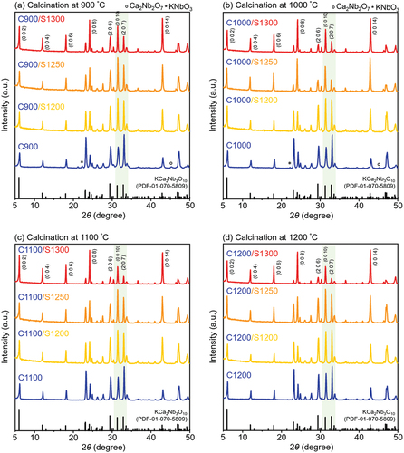
The XRD patterns of “C900” and “C1000” contain secondary peaks corresponding to Ca2Nb2O7 (marked with a circle symbol in and KNbO3 (marked with a star symbol in . However, the KCNO powders calcined at temperatures higher than 1000°C (“C1100” and “C1200” in are all single phase. The single-phase KCNO is synthesized via a two-step process. From the starting materials (K2CO3, CaCO3, and Nb2O5), intermediate phases like Ca2Nb2O7 and KNbO3 are formed first. The intermediate phases will then react to synthesize KCNO [Citation23].
Previously, the intermediate phases were formed at temperatures near 500°C, and their phases could still be detected even when the starting materials were calcined at 700°C [Citation24]. According to the chemical reaction (1), the secondary peaks detected in “C900” and “C1000” correspond to intermediate phases (Ca2Nb2O7 and KNbO3) that have not been reacted to form KCNO. From the single-phase XRD patterns of “C1100” and “C1200”, it can be inferred that the complete reaction of the intermediate phases is possible if the calcining temperature is greater or equal to 1100°C. Once the calcined KCNO powders are sintered at temperatures ranging from 1200°C to 1300°C, all the KCNO samples become phase pure. Even the Ca2Nb2O7 and KNbO3 in “C900” and “C1000” powders react to form single-phase KCNO after sintering. The effect of calcination temperature increase observed in the XRD patterns is a relative intensity increase of peaks corresponding to (0 0 l) planes. In particular, the relative peak intensity of (0 0 10) plane (2θ ~31.45°) in reference to the peak corresponding to (2 0 7) plane (2θ ~33°) increases as the calcination temperature increases. However, the amount of increase in the intensity of (0 0 10) peak relative to (2 0 7) is only incremental.
When the sintering temperature is increased (at the same calcination temperature), the peaks corresponding to (0 0 l) planes increase significantly. If we take “C900” in as an example, its peak intensity of (0 0 10) plane was initially lower than that of (2 0 7) (highlighted in green). However, as the “C900” powder is sintered at 1200 (“C900/S1200”), 1250 (“C900/S1250”), and 1300°C (“C900/S1300”), the corresponding (0 0 10) peaks become higher than (2 0 7) peaks according to . Regardless of the calcination temperature, samples sintered at 1300°C exhibit the most drastic increase in (0 0 10) peak intensity relative to (2 0 7) peak intensity. When the XRD pattern of “C900/S1300” in is compared to that of “C1200/S1300” in , the intensity of (0 0 10) peak is much higher than that of (2 0 7) as the calcination temperature increased. Therefore, increases in both calcining and sintering temperatures can promote preferential grain growth along (0 0 l) planes.
shows how the microstructure of the fractured KCNO bulk sample changes with different calcining and sintering temperatures. The calcining temperature of the sample increases as we move from the SEM image on the left to that on the right, and if they are on the same row, the corresponding samples are sintered at the same temperature. For example, are both on the same row. The calcining temperature for the sample in is 900°C, while that in is 1200°C. Both samples in were sintered at 1200°C. Hence, we indicated “C900/S1200” and “C1200/S1200” for respectively. The sintering temperature of the sample increases as we move down the column of the SEM images (but the calcining temperature is kept constant). If we compare (“C900/S1200”) and 2(i) (“C900/S1300”) that are in the same column, the sample in was sintered at 1200°C, while that in was sintered at 1300°C.
Figure 2. Scanning Electron Microscope (SEM) images of fractured KCNO bulk samples prepared via calcining (900°C–1200°C) and subsequent sintering processes (1200°C–1300°C).
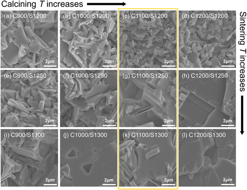
The difference between calcining and sintering temperatures has an impact on the microstructure of the fractured sample. The “C900/S1200” sample shown in has a 300°C difference between the calcining and sintering temperatures, but the “C1200/S1200” sample was sintered at the same temperature at which its powder was calcined. For this reason, the average grain size observed in “C900/S1200” () looks larger than that observed in “C1200/S1200” (). When the difference between the calcining and sintering temperatures is small, the driving force for further grain growth resulting from particle coalescing is limited. However, when the sintering temperature is as high as 1300°C (), the difference between calcining and sintering temperatures does not affect the final microstructure as strongly as it would when the sintering temperature is only 1200°C. When the microstructures of “C1000/S1300” () and “C1200/S1300” () are compared, the grains observed in “C1000/S1300” and “C1200/S1300” seem to be similarly large. Even if the difference between the calcining and sintering temperatures in “C1200/S1300” (100°C difference) is only one-third of that set in “C1000/S1300” (300°C difference), the sintering temperature of 1300°C is high enough to maximize grain growth regardless of the initial particle size of the powder [Citation26,Citation27].
The grain growth during sintering is closely connected to the density of the samples. shows the relative densities of KCNO-sintered samples as functions of calcining and sintering temperatures (). The relative densities of the samples sintered at the same temperature are presented with the same color. For example, the square prisms in yellow, orange, and red represent the relative densities of the samples sintered at 1200°C, 1250°C, and 1300°C, respectively. According to , 1300°C sintering promoted significant grain growth in the KCNO samples regardless of the calcining temperatures. This observation can also be confirmed in . The samples sintered at 1300°C have the highest relative densities among other samples (>95%). Plus, the difference in the relative densities of the samples calcined at different temperatures is the smallest when the sintering temperature is 1300°C.
Figure 3. (a) Relative densities of KCNO-sintered samples for different calcining and sintering temperatures. Electron backscatter diffraction (EBSD) image quality (IQ) maps of KCNO powders calcined at 1100°C followed by sintering at (b) 1200°C, (c) 1250°C, and (d) 1300°C.
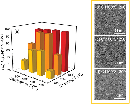
Table 1. Relative densities (in g cm−3) of KCNO for varying calcining and sintering temperatures.
However, for the samples sintered at temperatures lower than 1300°C, the difference between the calcining and sintering temperatures, particle size, and even the particle size distribution of the calcined powder may also play a role in determining the relative density of the sintered samples. When the calcining and sintering temperatures are the same as in “C1200/S1200” (in , the densification via particle rearrangement and surface diffusion is suppressed (<75% in . The low relative density of “C900/S1200” (yellow square prism in ), despite the more rapid grain growth observed in , may be attributed to a broad particle size distribution of calcined powders [Citation28]. Overall, the samples initially calcined at 1000°C and 1100°C exhibited much higher sintered densities than those calcined at 900°C or 1200°C when sintered at temperatures lower than 1300°C.
) in the yellow box shows the electron backscatter diffraction (EBSD) image quality (IQ) maps of KCNO powders calcined at 1100°C and subsequently sintered at 1200°C–1300°C. Microstructures of fractured surfaces observed in (also in the yellow box) correspond to IQ maps observed in , respectively. While we can only infer approximate grain sizes of a sample relative to other samples with different calcining/sintering temperatures from fractured surfaces in , the IQ maps in ) provide accurate information on the morphology and size of the grains. According to the IQ map, samples first calcined at 1100°C and subsequently sintered at temperatures higher than 1200°C have elongated grains. The length of the grain along the elongated direction significantly increases with an increasing sintering temperature. For example, the average length of the grain along the elongated direction of “C1100/S1200” (), “C1100/S1250” (), and “C1100/S1300” () is approximately 3, 10, and 18 μm, respectively. The aspect ratios of the elongated grains also increase as the sintering temperature increases. Given that the average width of the elongated grains in “C1100/S1300” () is only approximately 1.5 μm, the aspect ratio of the elongated grains observed in “C1100/S1300” () amounts to 12. However, the aspect ratio of the elongated grains in “C1100/S1200” () is only about 3. More than a factor of 4 increase in the aspect ratio of elongated grains is obtained when the sintering temperature is increased from 1200°C to 1300°C. This increase in the aspect ratio of the elongated grains also supports the preferential grain growth along (0 0 l) plane confirmed by the XRD analysis in .
shows the temperature-dependent dielectric properties of the KCNO samples calcined (900–1200°C) and subsequently sintered (1200°C–1300°C) at various temperatures (). The temperature-dependent dielectric properties were measured from room temperature to 200°C. All the measurements were taken at 1 kHz (0 DC bias and 1 Vrms). , show dielectric constants (ε) and loss tangent (tan δ) of the sintered KCNO samples which first calcined at 900°C (triangle), 1000°C (square), 1100°C (pentagon), and 1200°C (circle symbols), respectively. Dielectric properties of the samples sintered at 1200°C, 1250°C, and 1300°C, are presented in yellow, orange, and red solid lines in .
Figure 4. Temperature-dependent dielectric constants (ε) and loss tangent (tan δ) of the KCNO samples calcined at (a) 900°C, (b) 1000°C, (c) 1110°C, and (d) 1200°C, followed by sintering at temperatures from 1200°C to 1300°C, measured at 1 kHz (0 direct current (DC) bias and 1 Vrms).
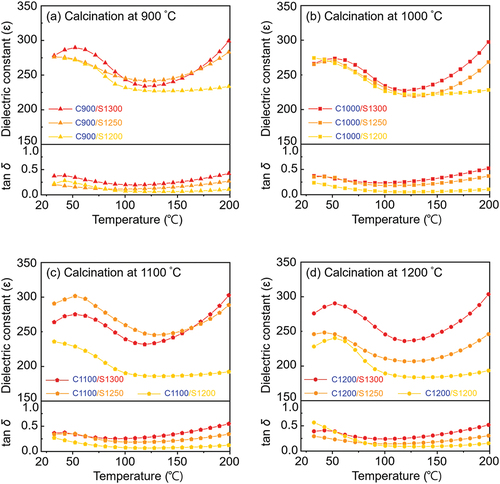
Table 2. Dielectric constants of KCNO samples at 25°C for varying calcining and sintering temperatures.
The calcining and sintering temperatures also affect the temperature-dependent ε of the KCNO samples. First of all, calcining temperature changes the impact of sintering temperatures on the ε at temperatures below 115°C (115°C is where the ε is at its maximum except for the samples sintered at 1200°C). For the calcining temperatures 900°C and 1000°C (), the discrepancies in ε with different sintering temperatures are negligible. However, for the calcining temperatures 1100°C and 1200°C ()), the discrepancies in ε with different sintering temperatures become significant. For example, the room temperature ε of the samples calcined at 900°C and 1000°C are all approximately 275. However, those of the samples calcined at 1100°C and 1200°C span from 225 (“C1200/S1200” in ) to 290 (“C1100/S1250” in . The dielectric constants of the samples can be understood in terms of their average grain sizes () and relative densities (). The difference in grain size observed in fractured samples “C900/S1200” () and “C900/S1300” () is not significant, but that observed between “C1200/S1200” () and “C1200/S1300” () is significant. While the large grain size obtained in “C900/S1200” compensates for its low relative density () and exhibits a high ε that is comparable to that of “C900/S1300” in , the small grain size of “C1200/S1200” combined with its also low relative density () exhibits an ε that is lower than that of “C1200/S1300” in .
Second, the sintering temperature determines the rate of ε change with the temperature at temperatures higher than 115°C. Regardless of the calcining temperature, the rate of ε increase increases with an increasing sintering temperature. The ε of the samples sintered at 1200°C does not change with temperature for temperatures higher than 115°C. However, the rates of ε increase for the samples sintered at 1250°C and 1300°C are 0.8°C−1 and 1.1°C−1, respectively. Approximately 38% increase in the rate of ε increase is observed as the sintering temperature is increased from 1250°C to 1300°C. It is also to be noted that the 200°C ε of the samples sintered at 1300°C is all ~300 regardless of the calcining temperature. This observation supports that the sintering at 1300°C maximizes the grain growth ()) and relative density (), which are closely related to the ε.
The overall trend of the temperature-dependent tan δ resembles that of the temperature-dependent ε. In general, the higher the sintering temperature, the higher the tan δ. However, the highest tan δ of the samples calcined at different temperatures all coincide with being approximately 0.5. The rate of tan δ increase also increases with an increasing sintering temperature at temperatures higher than 115°C. The tan δ of the samples sintered at 1200°C does not change with an increasing temperature at temperatures higher than 115°C. The tan δ is expressed as a ratio of ε to the dielectric loss factor, which represents the ability of a material to dissipate the absorbed energy into heat. Because the ε of the samples sintered at 1200°C does not change with an increasing temperature at temperatures higher than 115°C as well, the constant tan δ at temperatures higher than 115°C indicates that the dielectric loss factors for the samples sintered at 1200°C are also approximately constant with temperatures at >115°C.
shows the temperature coefficient of capacitance (TCC) of the KCNO samples calcined and sintered at different temperatures (). The TCC presented in are calculated using the temperature-dependent ε of the KCNO samples provided in using the following EquationEquation (2)(2)
(2) [Citation29].
Figure 5. Temperature coefficient of capacitance (TCC) of the KCNO samples calcined at (a) 900°C, (b) 1000°C, (c) 1110°C, and (d) 1200°C, followed by sintering at temperatures from 1200°C to 1300°C, measured at 1 kHz.
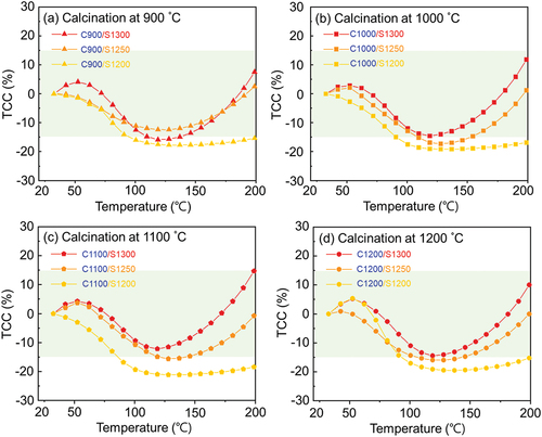
Table 3. Temperature Coefficient of Capacitance (TCC in %) of KCNO samples for varying calcining and sintering temperatures.
The εT and ε25 in EquationEquation (2)(2)
(2) are the dielectric constants at temperature T (in Celsius) and at 25°C, respectively. The green-shaded region in presents the TCC being equal to or less than ± 15%.
The sintering temperature is a more critical factor that determines the TCC of the KCNO samples than the calcining temperature. According to , the TCC of the samples sintered at the same temperature was all comparable regardless of their calcining temperature. For example, the TCC of “C900/S1200” (), “C1000/S1200” (), “C1100/S1200” (), and “C1200/S1200” () decrease to approximately −20% near 100°C and stay more or less the same up to 200°C. The TCC of the samples sintered at 1300°C has their minimum of approximately −15% near 120°C, and they reach the TCC of 10% or higher at 200°C. Except for the samples calcined at 900°C, those samples sintered at 1300°C have the TCC changing by less than ± 15% at temperatures ranging from 25°C to 200°C. For the samples calcined at 900°C, only the sample sintered at 1250°C (“C900/S1250” in has the TCC varying less than ± 15%. The reason that the TCC of the samples sintered at 1300°C could fall between ± 15% is a rapid increase in TCC starting from 120°C. Again, the rate of TCC increase with the temperature of the samples sintered at 1300°C is the highest among other samples sintered at lower temperatures. It is also to note that only the samples whose sintered grains are significantly elongated (as observed in “C1100/S1300” in have the TCC varying less than ± 15% at temperatures as high as 200°C.
shows the temperature-dependent AC conductivities (σac) of “C1100/S1200”, “C1100/S1250”, and “C1100/S1300”. The σac is obtained from the measured temperature-dependent ε and tan δ according to EquationEquation (3)(3)
(3) [Citation30].
Figure 6. Temperature-dependent AC conductivities (σac) of the KCNO samples calcined at 1100°C, followed by sintering at temperatures from 1200°C to 1300°C, at 1 kHz.
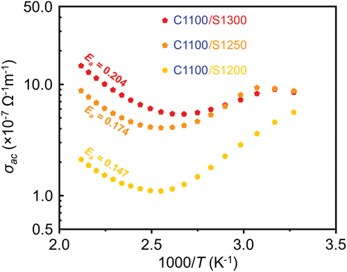
The ε0 and ω in equation. (3) are the vacuum permittivity and the frequency, respectively. Because we want to compare the σac of the samples sintered at different temperatures, the ω is kept constant to be 1 kHz. In contrast to , the temperatures in are in absolute temperatures (in the unit of K). Therefore, the 1000/T (K−1) being less than 2.5 in corresponds to a temperature higher than approximately 127°C in . In other words, as the temperature increases from 127°C (as 1000/T (K−1) decreases from 2.5), the σac of all the samples calcined at 1100°C also increase. Among the samples calcined at 1100°C, the σac of the samples sintered at higher sintering temperatures increases more rapidly with increasing temperature. The change in σac with temperature (in Kelvin) can, in turn, be explained in terms of the activation energy (Ea) as shown in Eq. (4).
The σ0 and kB in the Arrhenius equation (EquationEquation 4(4)
(4) ) are the pre-exponential factor and Boltzmann constant, respectively. The Ea in EquationEquation (4)
(4)
(4) is fitted to the change in σac for 1000/T (K−1) less than 2.5, and the estimated Ea of “C1100/S1200”, “C1100/S1250”, and “C1100/S1300” are 0.147, 0.174, and 0.204 eV, respectively. The highest Ea of the sample sintered at 1300°C can be related to the rapid increase in ε with increasing temperature which ensures its TCC being less than ± 15% at temperatures ranging from 25°C to 200°C. In terms of the microstructure, highly elongated grains may be necessary to obtain the highest Ea among other samples sintered at temperatures lower than 1300°C.
4. Conclusions
In summary, the impact of changing calcining and sintering temperatures on the temperature coefficient of capacitance (TCC) of KCa2Nb3O10 (KCNO) samples was studied. The KCNO samples sintered at 1300°C exhibited a strong preferential grain growth along (0 0 l) planes, irrespective of their calcining temperatures ranging from 900°C to 1200°C. For the KCNO samples initially calcined at 1100°C, increasing subsequent sintering temperature from 1200°C to 1300°C significantly increased the aspect ratio of the elongated grains by up to a factor of 4. The samples sintered at 1300°C exhibited the highest dielectric constant (ε) at temperatures from 25°C to 200°C, regardless of calcining temperature. In particular, the rate of ε increase with temperature at temperatures higher than 120°C was also the highest for the samples sintered at 1300°C. The activation energy (Ea) of the samples sintered at 1300°C was also estimated to be the highest at temperatures higher than 120°C. The high Ea of the 1300°C-sintered samples is closely related to the TCC of the 1300°C-sintered samples being less than ± 15% at temperatures from 25°C to 200°C. In terms of microstructure, highly elongated grains may be responsible for the high Ea of the 1300°C-sintered samples. The KCNO samples whose TCC can be engineered with microstructure control have a great potential to be applied to multilayer ceramic capacitors for electric vehicles as a dielectric material.
Acknowledgments
This work was supported by the National Research Foundation of Korea (NRF) grant funded by the Korean government (MSIT) (RS-2023-00212959). This research was also supported by the Basic Science Research Program through the National Research Foundation of Korea (NRF) funded by the Ministry of Education (NRF-2019R1A6A1A11055660), and the Technology Innovation Program RS-2022-00144027 funded by the Ministry of Trade, Industry & Energy (MOTIE, Korea).
Disclosure statement
No potential conflict of interest was reported by the authors.
Additional information
Funding
References
- Hong J-O, Kim S-H, Hur K-H. development history and trend of high-capacitance multi-layer ceramic capacitor in Korea. J Korean Ceram Soc. 2009;46(2):161–169. doi: 10.4191/KCERS.2009.46.2.161
- Hong K, Lee TH, Suh JM, et al. Perspectives and challenges in multilayer ceramic capacitors for next generation electronics. J Mater Chem C. 2019;7(32):9782. DOI:10.1039/C9TC02921D
- Wang S-F, Li JH, Hsu Y-F, et al. Dielectric properties and microstructures of non-reducible high-temperature stable X9R ceramics. J Eur Ceram Soc. 2013;33:1793–1799. doi: 10.1016/j.jeurceramsoc.2013.02.021
- Do TV, Trovão JPF, Li K, et al. Wide-bandgap power semiconductors for electric vehicle systems. IEEE Veh Technol Mag. 2021;16(4):89–98. doi: 10.1109/MVT.2021.3112943
- Zeb A, Miline SJ. High temperature dielectric ceramics: a review of temperature-stable high-permittivity perovskites. J Mater Sci. 2015;26(12):9243–9255. doi: 10.1007/s10854-015-3707-7
- Pithan C, Hennings D, Waser R. Progress in the synthesis of nanocrystalline BaTiO3 powders for MLCC, applied ceramic technology. Int J Appl Ceram Technol. 2005;2(1):1–14. doi: 10.1111/j.1744-7402.2005.02008.x
- Kim C-H, Park K-J, Yoon Y-J, et al. Role of yttrium and magnesium in the formation of core-shell structure of BaTiO3 grains in MLCC. J Eur Ceram Soc. 2008;28:1213–1219. doi: 10.1016/j.jeurceramsoc.2007.09.042
- Mizuno Y, Kishi H, Ohnuma K, et al. Effect of site occupancies of rare earth ions on electrical properties in Ni-MLCC based on BaTiO3. J Eur Ceram Soc. 2007;27(13–15):4017–4020. DOI:10.1016/j.jeurceramsoc.2007.02.089
- Politai AV, Yang G-Y, Dickey EC, et al. utilization of multiple-stage sintering to control ni electrode continuity in ultrathin Ni?BaTioO3 multilayer capacitors. J Am Ceram Soc. 2007;(0):3811–3817. doi: 10.1111/j.1551-2916.2007.02058.x
- Smith MB, Page K, Siegrist T, et al. Crystal structure and the paraelectric-to-ferroelectric phase transition of nanoscale batiO3. J Am Chem Soc. 2008;130(22):6955–6963. DOI:10.1021/ja0758436
- Ravel B, Stern EA, Vedrinski RI, et al. Local structure and the phase transitions of BaTiO3. Ferroelectrics. 1998;206(1):407–430. DOI:10.1080/00150199808009173
- Schlag S, Eicke H-F. Size driven phase transition in nanocrystalline BaTiO3. Solid State Commun. 1994;91(11):883–887. doi: 10.1016/0038-1098(94)90007-8
- Sato S, Fujikawa Y, Nomura T. Effect of rare-earth doping on the temperature-capacitance characteristics of mlccs with ni electrodes. J Ceram Soc Jpn. 2004;112:S481–S485.
- Tang B, Zhang S, Zhou X, et al. Regression analysis for complex doping of x8r ceramics based on uniform design. J Electron Mater. 2007;36(10):1383–1388. doi: 10.1007/s11664-007-0271-9
- Wada N, Hiramatsu T, Tamura T, et al. Investigation of grain boundaries influence on dielectric properties in fine-grained BaTiO3 ceramics without the core–shell structure. Ceram Int. 2008;34(4):933–937. doi: 10.1016/j.ceramint.2007.09.061
- Yao G, Wang X, Wu Y, et al. Nb-doped 0.9batio3-0.1(bi0.5na0.5)tio3 ceramics with stable dielectric properties at high temperature. J Am Ceram Soc. 2012;95(2):614–618. doi: 10.1111/j.1551-2916.2011.04793.x
- Xu O, Huang D-P, Chen M, et al. Effect of bismuth excess on ferroelectric and piezoelectric properties of a (Na0.5bi0.5)tio3–BaTiO3 composition near the morphotropic phase boundary. J Alloys Compd. 2009;471(1–2):310–316. doi: 10.1016/j.jallcom.2008.03.078
- Chu B-J, Chen D-R, Li G-R, et al. Electrical properties of Na1/2Bi1/2TiO3–BaTiO3 ceramics. J Eur Ceram Soc. 2002;22(13):2115–2121. doi: 10.1016/S0955-2219(02)00027-4
- Gao S, Wu S, Zhang Y, et al. Study on the microstructure and dielectric properties of X9R ceramics based on BaTiO3. Mater Sci Eng B. 2011;176:68–71. doi: 10.1016/j.mseb.2010.09.004
- Li L-X, Han Y-M, Zhang P, et al. Synthesis and characterization of BaTiO3-based X9R ceramics. J Mater Sci. 2009;44(20):5563–5568. DOI:10.1007/s10853-009-3779-y
- Scaak RE, Mallouk TE. Perovskites by design: a toolbox of solid-state reactions. Chem Mater. 2002;14(4):1455–1471. doi: 10.1021/cm010689m
- Han Y-S, Park I, Choy J-H. Exfoliation of layered perovskite, KCa2Nb3O10, into colloidal nanosheets by a novel chemical process. J Mater Chem. 2001;11(4):1277–1282. doi: 10.1039/b006045n
- Kweon S-H, Im M, Han G, et al. Sintering behavior and dielectric properties of KCa2Nb3O10 ceramics. J Eur Ceram Soc. 2013;33(5):907–911. DOI:10.1016/j.jeurceramsoc.2012.11.017
- Kim J-Y, Lim J-C, Kim S-I, et al. Impact of two-step calcination on microstructure, phase, electronic, and dielectric properties of KCa2Nb3O10 bulk layered perovskite. J Asian Ceram Soc. 2023;11(1):188–196. DOI:10.1080/21870764.2023.2174243
- Osada M, Sasaki T. Two-dimensional dielectric nanosheets: novel nanoelectronics from nanocrystal building blocks. Adv Mater. 2012;24(2):210–228. doi: 10.1002/adma.201103241
- Li W, Gao L. Compacting and sintering behavior of nano ZrO2 powders. Scripta Materialia. 2001;44(8–9):2269–2272. doi: 10.1016/S1359-6462(01)00753-9
- Kara F, Little JA. Sintering behavior of precursor mullite powders and resultant microstructures. J Eur Ceram Soc. 1996;16(6):627–635. doi: 10.1016/0955-2219(95)00179-4
- Ting J-M, Lin RY. Effect of particle size distribution on sintering. J Mater Sci. 1995;30(9):2382–2389. doi: 10.1007/BF01184590
- Dean JS, Foeller PY, Reaney JM, et al. A resource efficient design strategy to optimise the temperature coefficient of capacitance of BaTiO3-based ceramics using finite element modelling. ?J Mater Chem A. 2016;4(18):6896. doi: 10.1039/C5TA09573E
- Pradhani N, Mahapatra PK, Choudhary RNP. Effect of cerium oxide addition on optical, electrical and dielectric characteristics of (Bi0.5Na0.5)TiO3 ceramics. JPhys Materials. 2018;1(1):015007. doi: 10.1088/2515-7639/aacff0