
 ?Mathematical formulae have been encoded as MathML and are displayed in this HTML version using MathJax in order to improve their display. Uncheck the box to turn MathJax off. This feature requires Javascript. Click on a formula to zoom.
Abstract
Objective of this paper is to investigate the transient response of a PV module irradiated by an impulse light flash. The impulse flash with a waveform of 8/20 μs was considered. LTSpice was employed for the numerical simulation. Based on the numerical results, the short-circuit current and the electrical properties of some cell components (such as the diode, capacitance and inductance) are demonstrated and discussed. It is found that the irradiation by the pulsed flash causes not only the oscillation of the short-circuit current, but also the oscillation of voltage and current of cell components, depending both on the capacitance C of the PV cell and on the inductance L of wiring and cables. It is also found that, under a certain condition of L and C, the diode voltage becomes negative; namely, application of the large reverse voltage to the cell is pointed out. It is concluded that the response of the PV module against the pulsed photo-current is composed of two sequential stages; the first stage is a charging stage of C by the pulsed photo-current, and the next stage is a discharging stage of C. The latter stage causes a damping oscillation of short-circuit current.
Introduction
Nowadays, the more and more growing interest in applications of photovoltaic (PV) generation, with all the related problems of optimal exploitation, environmental impact, and grid stability, has determined a speedup of the research in this field [Citation1]. High risk of damage and low performance of solar panel can be caused by both of direct and indirect lightning stroke which is one of the environment impacts of Photovoltaic (PV) generation. Researchers are interesting to study the phenomenon of lighting and electrical characteristics flowing in solar cell components [Citation2].
The PV module produces current and voltage that depends on the irradiation from sunlight or lightning flash and on all the components of solar cell. Many studies and researches already done prove that the capacitance and inductance of solar cells have a strong effect on electrical characteristics on PV solar panels [Citation3]. IEC (International Electro-Technical Commission) standards considered two types of current wave form 10/350 μs which characterize the current wave from direct lightning stroke and 8/20 μs which characterize the current wave from indirect lightning stroke. The impulse light flash which has current waves form 8/20 μs was considered in this paper.
The objective of this simulation is to obtain the transient electrical behaviour of current and voltage for each solar cell component, as well as whole electrical characteristics of a PV module such as the short-circuit current, provided that a pulsed photo-current is generated in the PV module when a PV module is irradiated by an impulse lightning flash. LT spice [Citation4] is employed in the simulation. In this paper, based on the numerical results, the short-circuit current and the electrical properties of some cell components (such as the diode, capacitance and inductance) are demonstrated and discussed.
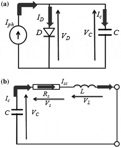
Electrically equivalent circuit of a single solar cell
A solar PV module is composed by connecting many solar cells in series. In the present simulation, the solar cell is represented by one diode-model and their components. The electrically equivalent circuit of a single solar cell containing all the parameters explained in below is shown in .
Figure 1. Electrically equivalent circuit of a short-circuit solar cell employed in the transient analysis.
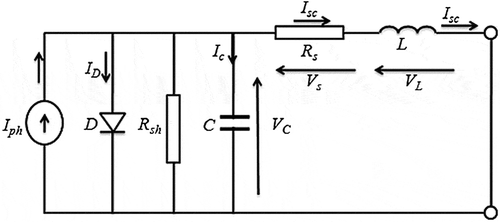
where I ph is a pulsed photo-current generated by the irradiation of an impulse light flash, D is a diode that has the same behaviour as a p-n junction of the solar cell, R s is a series resistance of the cell, R sh is a shunt resistance of the cell, C is a parasitic capacitance of the cell, cables and stray capacitance, L is a parasitic inductance of the wiring on the cell surface and cables. It is assumed that the waveform of the photo-current is the same as that of the external flash.
Based on this model, the following relationships are obtained for the currents and voltages.
The parameters used in a single solar cell are shown in . The values of I S , n, R sh are delivered from the reference [Citation4], and R s from the reference [Citation5]. C 0 is a cell capacitance obtained in the steady-state operation [Citation6], A is an area of the solar cell. The value of L 0 is a suggestion by the authors.
Table 1. Values of parameters of a solar cell used in simulation.
The electrical characteristics of all components were calculated using LTspice, provided that the current I sh of the shunt resistance was negligibly small. The solar cell employed in this simulation had the rated photo-current I ph = 8 A, the short-circuit current I sc = 4.2 A and the open-circuit voltage V oc = 0.59 V.
In this simulation, a waveform of the pulsed photo-current was described as the double exponential mathematical expression as shown in Equation (3).
where α and β are formula constants and remain to be determined for the lightning impulse current waveform, and I is a parameter regarding a maximum current.
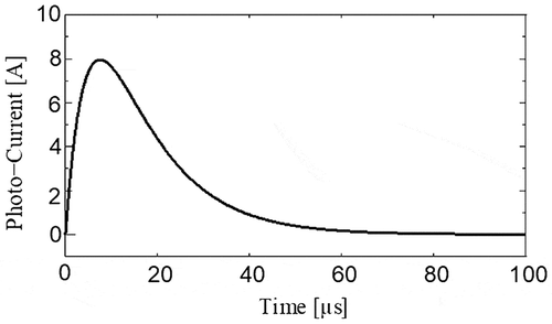
In this simulation, the waveform of 8/20 μs was used for the impulse photo-current, which is the same waveform as the standard lightning current. shows the dependency of the photo-current on time, which has maximum magnitude of I ph = 8 A.
Figure 2. Waveform of the impulse photo-current of 8/20 μs used in the simulation.
Effects of capacitance and inductance
In this chapter, the voltages of the diode and inductance are represented by V D and V L, respectively. The diode current, capacitance current, and short-circuit current are represented by I D, I C, and I SC, respectively. The impulse photo-current shown in is represented by I ph.
Base values of capacitance and inductance
Two parameters of C 0 = 50 nF/cm2 × 78.5 cm2 = 3.9 μF (see ) and L 0 = 1 μH are used to give the base values of the capacitance and inductance, respectively. The value of L 0 is a suggestion by the authors.
Values of V D and V L as a function of time, which were obtained for C = C 0 = 3.9 μF and L = L 0 = 1 μH, are shown in . shows that the irradiation by the pulsed flash light causes the oscillation of V D and V L as a function of time, and the times when both V D and V L become maximum are different from that of the photo-current. It is also clear from that V D is always positive, while V L has the positive peak magnitude followed by the negatively oscillating voltages.
Figure 3. Diode and inductance voltages as a function of time for C = 3.9 μF and L = 1 μH.
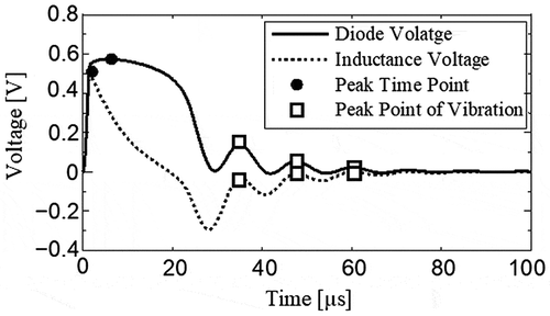
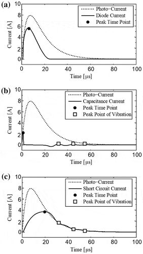
Figure (a)–(c) show I D, I C, and I SC as a function of time, respectively, which were obtained for C = C 0=3.9 μF and L = L 0 = 1 μH. It is seen from that I SC has smaller magnitude than I ph until it reaches the maximum value, and that the peak time when the peak magnitude of I SC takes place lags from that of I ph.
Figure 4. Currents as a function of time for C = 3.9 μF and L = 1 μH. (a) Diode current. (b) Capacitance current. (c) Short circuit current.
Effects of change in capacitance
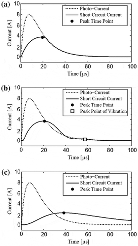
Figure (a)–(c) show change in I sc as a function of time for C = 0.39 μF, 19.5 μF and 390 μF, respectively. Changes in I sc obtained for C = 3.9 μF are shown in the previous . The value of L was kept being 1 μH for all cases. Figures and show that the magnitude of I sc monotonously decreases as C becomes larger. The time when the magnitude of I sc becomes maximum is lagged than that of I ph in all cases, and the amount of lagged time becomes larger as C becomes larger.
Figure 5. Dependency of short-circuit current on time when a cell capacitance C is varied. (a) C = 0.39 μF, L = 1 μH. (b) C = 19.5 μF, L = 1 μH. (c) C = 390 μF, L = 1 μH.
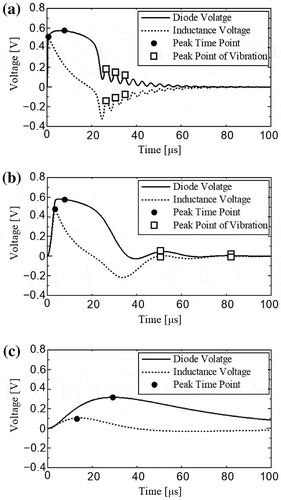
Values of V D and V L as a function of time for C = 0.39 μF, 19.5 μF and 390 μF are shown in Figure (a)–(c), respectively. Those for C = 0.39 μF are shown in the previous . The value of L was kept being 1 μH for all cases. It is clear from Figures and that, although both V D and V L oscillate with time for all cases examined, the oscillation continues for longer time as C becomes larger. The negative values of V L are significantly larger for smaller C. It is also obvious from Figures and that the times when both V D and V L become maximum lag more as C becomes larger.
Figure 6. Diode and inductance voltages as a function of time when a cell capacitance C is varied. (a) C = 0.39 μF, L = 1 μH. (b) C = 19.5 μF, L = 1 μH. (c) C = 390 μF, L = 1 μH.
Effects of change in inductance
Values of I SC as a function of time are shown in Figure (a)–(c) for L = 0.5 μH, 5 μH and 100 μH, respectively. I SC for L = 1 μF is shown in the previous . The value of C was kept being 3.9 μF for all cases. It is seen from Figures and that the maximum magnitude of I SC decreases as L increases. It is also clear that I SC starts to oscillate when L is larger than 1 μH.
Figure 7. Dependency of short-circuit current on time when a cell inductance L is changed. (a) C = 3.9 μF, L = 0.5 μH. (b) C = 3.9 μF, L = 5 μH. (c) C = 3.9 μF, L = 100 μH.
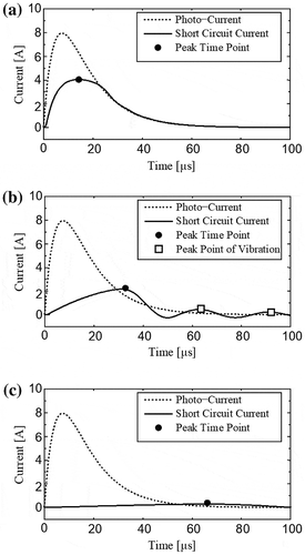
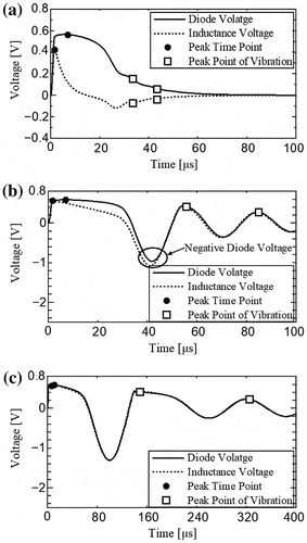
Figure (a)–(c) show V D and V L as a function of time for L = 0.5 μF, 5 μF and 100 μF, respectively. Those for L = 1 μF are shown in the previous . The value of C was kept being 3.9 μF for all cases. It is obvious from Figures and that the values of V D and V L oscillate as a function of time, and that the dependency of V D and V L on time almost coincide each other in case of larger inductances (i.e. L = 5 μF or more). It is noted that V D becomes negative in case of larger inductances (i.e. L = 5 μF or more), and that the negative values of V D become larger with the inductance. The occurrence of the negative diode voltage pointed out that the large reverse voltage to the cell is applied under a certain condition of L and C.
Figure 8. Diode and inductance voltages as a function of time when a cell inductance L is varied. (a) C = 3.9 μF, L = 0.5 μH. (b) C = 3.9 μF, L = 5 μH. (c) C = 3.9 μF, L = 100 μH.
Discussion
The numerical results shown in Figures – demonstrate that the oscillation of the short-circuit current and capacitance current begin after the pulsed response of the diode current and voltage is almost closed to the end.
The magnitude and time when the maximum values of the diode current I D, capacitance current I C, short-circuit current I SC, diode voltage V D, and inductance voltage V L take place are read out from the simulation results shown in –, and are summarized in . indicates that the change in the capacitance have an influence both on the peak magnitude of I C, and on the peak times of I C and V L (see shaded cells in grey). Meanwhile, the change in the inductance have an influence both on the peak magnitudes of I D and I SC, and on the peak time of I SC and V L (see shaded cells in grey).
Table 2. The peak magnitude of various currents and voltages and the peak time when the peak magnitude takes place for various values of C and L. C 0 = 3.9 μF, L 0 = 1 μH.
To explain the transient response od a PV cell against the pulsed photo-current mentioned above, a simple mechanism is proposed and shown in . (a) shows a charging stage of the capacitance by the pulsed photo-current. The diode current is also supplied from the pulsed photo-current. In this charging stage, there is no oscillation of circuit voltage and current. Meanwhile, (b) shows a discharging stage of the capacitance, and, in this stage, the circuit voltage and current oscillate with the damping magnitude. The speed and frequency of the oscillation depend on the circuit components of series resistance R s , capacitance C and inductance L.
Figure 9. Two equivalent circuits of a single solar cell, which are representing two stages of charging and discharging process of the capacitance C. (a) Charging stage of the capacitance C. (b) Discharging stage of the capacitance C.
Conclusions
The transient electrical responses of a PV module are numerically investigated when an impulse photo-current of 8/20 μs is induced on the PV module by an impulse lightning flash. In this paper, numerical results on the short-circuit current and the electrical properties of some cell components (such as the diode, capacitance and inductance) are demonstrated and discussed.
Results obtained from the numerical analysis can be summarized as follows:
The irradiation by the pulsed flash causes not only the oscillation of the short-circuit current, but also the oscillation of voltage and current of cell components, depending both on the capacitance C of the PV cell and on the inductance L of wiring and cables.
Under a certain condition of L and C, the diode voltage becomes negative; namely, application of the large reverse voltage to the cell is pointed out.
The response of the PV module against the pulsed photo-current is composed of two stages; the first stage is a charging stage of C by the pulsed photo-current, and the sequential stage is a discharging stage of C. The latter stage causes a damping oscillation of short-circuit current.
Notes on contributors
Cheikh Ibra Wade (Master of Engineering) received Master of Engineering degree in 2017 from University of Miyazaki. He is now involved in the internship on the maintenance of power apparatus and their control systems in Kodensya co. Ltd., Nobeoka, Japan.
Ryo Torihara (Bachelor of Engineering) received Bachelor of Engineering degree in Electrical Engineering in 2002 from Kumamoto University. He is now a doctor course student of Interdisciplinary Graduate School of Agriculture and Engineering, University of Miyazaki, Japan. He is also a research staff of Miyazaki Prefecture Industrial Technology Center, Miyazaki, Japan. He is engaged in research on the development of on-line diagnosis technology for PV power plant, as well as in the technological support to local industrial companies.
Tatsuya Sakoda (Ph.D.) received his Ph. D. degree in Electrical Engineering from Kyushu University in 1998. He became a Research Associate, a lecturer and an Associate Professor in Sojo University in 1998, 2000, and 2005. He has been an Associate Professor in the University of Miyazaki since 2006 and Professor since 2013. His research interests include plasma engineering, high voltage engineering, and discharge engineering. He is members of Institute of Electrical Engineers of Japan, Institute of Electrical Installation Engineers of Japan.
Noriyuki Hayashi (Ph.D.) received his Ph.D. in Electrical Engineering in 1984 from Kyushu University. He is now a professor of University of Miyazaki, Japan. He is engaged in research on the electric power generation and transportation regarding the renewable energy, the electrical insulation and diagnosis of power apparatus, and the electrical coupling between human body and electromagnetic fields. He is members of IEEE/PES, IEEE/DEI, Institute of Electrical Engineers of Japan, Institute of Electrical Installation Engineers of Japan.
Funding
The work was supported in part by ABE Initiative special budget, JICA, Japan.
Acknowledgements
The authors are appreciated to help given by Prof. Otsubo, an alumni professor of University of Miyazaki.
References
- Di Piazza MC, Vitale G. Photovoltaic sources modelling and emulation. London: Springer-Verlag; 2013.10.1007/978-1-4471-4378-9
- Rahim NHA, Baharudin Z, Othman MdN. Investigation of wave propagation to PV-solar panel due to induced overvoltage generated by lightning impulse generator. Adv Sci Technol Lett. 2013;38:15–22.
- Eshappa T, Ranjan R, Ghatpande ND. Modelling of solar array and analyze the current transient response of shunt switch voltage regulator in spacecraft power conditioning unit. ISSN. 2015 April;3(2):2347–2804.
- Castaner L, Silvester S. Modelling photovoltaic systems using PSpice. England: Wiley; 2002.10.1002/0470855541
- Quaschningt V, Hanitscht R. Numerical simulation of current-voltage characteristics of photovoltaic systems with shaded solar cells. Solar Energy. 1996;56(6):513–520.10.1016/0038-092X(96)00006-0
- Kumar RA, Suresh MS, Nagaraju J. Effect of solar array capacitance on the performance of switching shunt voltage regulator. IEEE. 2016;21(2):543–548.